Note: Descriptions are shown in the official language in which they were submitted.
CA 02753575 2013-04-25
LOW DISSIPATION AMPLIFIER
BACKGROUND OF THE INVENTION
1) Field of the Invention
[0002] The field of the invention generally relates to amplifiers and, more
specifically, to an improved method to minimize distortion and power
dissipation in a
compact amplifier.
2) Background
[0003] Amplifiers are used for many applications including audio signal
processing,
video processing, communications, control systems, satellites, and so on.
Based on
its power consumption characteristics, an amplifier may be categorized into
one or
more categories including Class A, B, AB, D, G or H. A general background of
different amplifier classifications may be found, for example, in R. Bortoni,
et al.,
"Analysis, Design and Assessment of Class A, B, AB, G and H Audio Power
Amplifier
Output Stages Based on MATLAB Software," 110th Convention of Audio
Engineering Society (AES), May 12-15, 2001, pp. 1-14, and in "Audio Power
Amplification," J. Audio Eng. Soc, Vol. 54, No. 4, April 2006, pp. 319-323.
[0004] A Class A amplifier is known to require a relatively large amount of
standing
power and is inefficient, and thus undesirable in many applications that
require low
power dissipation. A Class B amplifier can have very low standing power
dissipation
but introduces distortion. A Class AB amplifier is somewhere between the two,
and
uses bias currents to reduce the distortion inherent in a Class B amplifier. A
Class AB
amplifier has a higher power dissipation than a Class B amplifier due to the
bias
currents.
- 1 -
CA 02753575 2013-04-25
[0005] As equipment gets smaller, amplifiers become an increasing limitation
on the
ability to reduce packaging size. The inevitable limited efficiency of an
amplifier leads
to power dissipation that must be dissipated by a heatsink in order to prevent
the
amplifier getting too hot; however, a large heatsink can take up an inordinate
amount
of packaging space. Techniques exist to improve the efficiency over that of a
standard Class AB amplifier design, and hence reduce heatsink requirements,
but
these approaches often lead to compromises in the bandwidth, noise or
distortion
performance of the amplifier.
[0006] There are at least two aspects to the power dissipation of an amplifier
system. The first is commonly known as idle or standing dissipation ¨ that is,
power
dissipated when the amplifier is delivering no power to the load. With a
conventional
linear amplifier, this standing dissipation, which includes the bias current
applied to
- 2 -
CA 02753575 2011-08-24
WO 2010/099349
PCT/US2010/025455
the amplifier, is primarily concentrated in the driver and output stage of the
amplifier
and is generally required in conventional amplifier designs to minimize
crossover
distortion. In a high performance audio power amplifier of a nominal 100 Watt
sine
wave power capability into an 8S2 load, for example, the idle current may be
of the
order of 100-200 milli-amps per channel. With a quiescent power supply voltage
of
typically +/-45 Volts, this idle current results in roughly 9-18 Watts of idle
power
dissipation per channel. This can be a significant problem for a stereo
amplifier, but
for a multi-channel amplifier it is an even larger problem, as the idle
dissipation
quickly becomes excessive as the number of amplifiers is increased.
[0007] For home audio amplifiers, large heatsinks can often be used to
dissipate
the power and keep the temperature of the power devices down, but for size-
constrained applications such as automotive entertainment systems, the size
and
weight of the heatsink cannot be tolerated.
[0008] The idle current for an amplification system must generally be set
at the
time of production for optimum distortion performance and thus increases
production
costs. The idle current requirements can also change with temperature and age.
Therefore, over time or after prolonged use, the quality of the amplifier
output may
deteriorate.
[0009] To add to the idle power dissipation problem, an amplifier produces
extra
dissipation, sometimes referred to as dynamic dissipation, when it is
delivering a
signal to the load. In practice, a nominal 100 Watt capability linear power
amplifier
may well dissipate 40 Watt worst case when delivering sine wave signals to a
load.
With music as the audio source for the amplifier, this figure is lower since
music has
a higher crest factor than sine waves, but may still approach 30 Watts per
channel.
- 3 -
CA 02753575 2011-08-24
WO 2010/099349
PCT/US2010/025455
[0010] Various techniques have been employed to reduce both the idle power
dissipation and the dynamic power dissipation of linear amplifiers. One
technique
that can be employed to reduce idle power dissipation is to decrease the
output
stage bias current. However, this causes crossover distortion to increase
which is
difficult to eradicate with conventional negative feedback around the
amplifier. Also,
this technique has little effect on the dynamic power dissipation.
[0011] Another approach that can reduce both idle and dynamic dissipation
is to
use a 'Class G' amplifier configuration. This 'Class G' nomenclature is
commonly
attributed to Hitachi (see "Highest Efficiency and Super Quality Audio
Amplifier Using
MOS Power FETs in Class G Operation," IEEE Transactions on Consumer
Electronics, Vol. CE-24, No. 3, August 1978), although the basic technique
appears
to have been described previously (see, e.g., U.S. Patent No. 3,622,899). A
'Class
G' amplifier arrangement maintains a lower voltage across the output devices
under
idle conditions whilst also reducing dynamic power dissipation by ensuring
that the
voltage across the power devices is also reduced when driving signals to the
load.
Thus both the idle and dynamic power dissipation is reduced. However, the
switching of the output devices between the power rails often causes glitches
in the
output waveform that appear as distortion. These glitches have significant
high
frequency energy and so are difficult to correct by negative feedback. Careful
design
can reduce this effect but cannot eliminate it and tends to increase high
frequency
dynamic power dissipation.
[0012] An alternative way of reducing amplifier dissipation is to implement
a
switching amplifier, and specifically a so-called 'Class D' architecture. With
this
design, the linear amplifier is replaced by power switches operating at
typically
- 4 -
CA 02753575 2011-08-24
WO 2010/099349
PCT/US2010/025455
several hundred kilohertz for a high performance audio amplifier. The nominal
efficiency of this design into a resistive load can theoretically be very
high, although
in practice switching losses and output filter losses significantly reduce the
actual
efficiency. The high switching frequency can cause significant EMI problems
which
then require bulky inductors to prevent coupling to power supply and output
lines, as
well as careful screening to avoid radiation. These additions mean that
although the
basic amplifier components can be small and low cost, the overall size is
significantly
larger and more costly due to the need for the inductive and filter
components.
Furthermore, the continual switching causes a significant idle current due to
the
dynamic switching losses and the pulse width modulation (PWM) process used to
generate the switching signal leads to a poor distortion performance compared
to a
linear amplifier.
[0013] An example of a Class D amplifier is the model TDF8590TH amplifier
available from NXP Semiconductors, a company headquartered in the Netherlands.
When this amplifier is configured to provide a nominal 100 Watt sine wave
power to
an 8S2 load, the idle dissipation is in excess of 4 Watts/channel. The total
harmonic
distortion (THD) is above 0.1% at 10kHz at all levels above 10 Watts output
and
rises dramatically at higher output levels¨and even these figures are an
underestimate of the actual distortion due to the use of an AES17 filter to
remove the
effect of the residual switching frequency components on the measuring
equipment.
The intermodulation distortion (IMD) performance is much worse than a well-
designed linear amplifier. The output inductors also generally must be large,
in order
that they do not saturate or introduce further distortion, and typically
measure 4 to 5
cubic centimeters, which is a barrier to overall circuit and package
miniaturization.
- 5 -
CA 02753575 2011-08-24
WO 2010/099349
PCT/US2010/025455
[0014] There remains a need therefore for an amplifier topology that can be
readily miniaturized while providing low power dissipation. There further is a
need
for an amplifier that is capable of providing low idle and dynamic power
dissipation
levels, requires no bias setting, and no inductors for EMI or filtering. There
further is
a need for an amplifier that delivers very low distortion levels.
SUMMARY OF THE INVENTION
[0015] According to one or more embodiments, a power amplifier system and
method is provided that may include one or more of the following features: a
distortion reducing topology; a Class AB driver stage; a current protection
mechanism; distortion reduction, especially when configured as a Class G or
Class
H amplifier; and a nested distortion reduction architecture.
[0016] According to an aspect of one or more embodiments, a low power, low
distortion amplifier comprises a first amplifier configured as or including a
driver
stage, and a second amplifier configured as or including a main output stage,
with a
plurality of impedance networks providing feedback paths from outputs of said
first
amplifier and said second amplifier to an input of said first amplifier, a
first coupling
path from the output of said second amplifier to a load, and a second coupling
path
from the output of said first amplifier to the load. The impedance networks
may be
resistors, capacitors, or network combinations thereof. An additional feedback
path
may be provided from the load to the input of the first amplifier. One or more
intermediate amplifier stage(s) may also be disposed between the first
amplifier and
the second amplifier.
- 6 -
CA 02753575 2013-10-09
[0017] According to another aspect of one or more embodiments, a method for
amplifying an input source signal comprises the steps of receiving the input
source
signal at a first amplifier and generating a driver signal thereby; providing
the driver
signal to the input of a second amplifier acting as a main output stage;
operating the
first amplifier in a Class AB or low power dissipation mode; operating the
second
amplifier in a Class B, Class G, Class H and/or low power dissipation mode;
and
providing selective coupling or feedback connections from the outputs of said
first and
second amplifiers to the inputs of said first and second amplifiers and to a
load to
maintain operation of said first and second amplifiers in their respective
modes.
[0018] According to yet another aspect of one or more embodiments as disclosed
herein, a low power, low distortion amplifier includes a plurality of cascaded
stages
with a driver stage biased to operate in Class AB mode, a main output stage
operating in a low power dissipation mode, and a plurality of impedance
networks
providing feedback paths or couplings between the outputs and inputs of the
cascaded stages or the load so that the amplifier provides low distortion and
maintains a substantially constant frequency response over a wide range of
frequencies. The low power amplifier may be configured to have very low
standing
and dynamic power dissipation.
[0019] According to certain embodiments or variations, the first amplifier may
operate in Class G or Class H mode.
[0019a] According to another aspect of one or more embodiments, there is
provided
an amplification system, comprising: a first amplifier for receiving an input
source
signal; a second amplifier downstream from the first amplifier; and a
plurality of
impedance networks providing (i) feedback paths from outputs of said first
amplifier
and said second amplifier to an input of said first amplifier, (ii) a first
coupling path
from the output of said second amplifier to a load, and (iii) a second
coupling path
from the output of said first amplifier to the load; wherein all of said
impedance
networks are comprised only of resistors, capacitors, or network combinations
of
- 7-
CA 02753575 2013-10-09
resistors and capacitors; and wherein at least one of said impedance networks
comprises a capacitor.
[0019b] According to another aspect of one or more embodiments, there is
provided
an amplification system, comprising: a first amplifier receiving an input
signal to be
amplified and supplied to a load; a second amplifier downstream from the first
amplifier, said second amplifier being operated in a low power dissipation
mode; a
feed-forward network coupling an output of said first amplifier to the load,
said feed-
forward network comprising a capacitor and a resistor connected in parallel; a
resistor
coupling said second amplifier to the load; and a plurality of negative
feedback paths
from the respective outputs of said first and second amplifiers to an input of
said first
amplifier.
[0019c] According to another aspect of one or more embodiments, there is
provided
a low dissipation amplifier, comprising: a driver amplifier for receiving an
input signal;
an output amplifier; a first impedance network Z1 coupling the output
amplifier to a
load; a second impedance network Z2 providing a feedback signal indicative of
an
output of the driver amplifier to an input of the driver amplifier; a third
impedance
network Z3 coupling the output of the driver amplifier to the load; and a
fourth
impedance network Z4 providing a feedback signal indicative of an output of
the
output amplifier to the input of the driver amplifier; wherein the third
impedance
network Z3 comprises a capacitor and a first resistor connected in parallel;
and
wherein the first impedance network comprises a second resistor.
[0019d] According to another aspect of one or more embodiments, there is
provided
a low dissipation amplifier, comprising: a driver amplifier coupled to an
input signal;
an output amplifier; a first impedance network Z1 coupling the output
amplifier to a
load; a second impedance network Z2 providing a feedback signal indicative of
an
output of the driver amplifier to an input of the driver amplifier; a third
impedance
network Z3 coupling the output of the driver amplifier to the load; and a
fourth
impedance network Z4 providing a feedback signal indicative of an output of
the
- 7a -
CA 02753575 2013-04-25
output amplifier to the input of the driver amplifier; wherein the values of
the first,
second, third and fourth impedance networks satisfy the relationship
Z1 (s).Z2(s)=Z3(s).Z4(s); wherein all of said impedance networks are comprised
only
of resistors, capacitors, or network combinations of resistors and capacitors;
and
wherein at least one of said impedance networks comprises a capacitor.
[0019e] According to another aspect of one or more embodiments, there is
provided
an amplification system, comprising: a first amplifier operable to receive an
input
source signal; a second amplifier connected downstream from the first
amplifier; a
first impedance network Z1 coupling the second amplifier to a load; a second
impedance network Z2 operative to provide a feedback signal indicative of an
output
of the first amplifier to an input of the first amplifier; a third impedance
network Z3
coupling the output of the first amplifier to the load at a common node with
the first
impedance network Z1; and a fourth impedance network Z4 operative to provide a
negative feedback signal indicative of an output of the second amplifier to
the input of
the first amplifier; wherein all of said impedance networks Z1, Z2, Z3 and Z4
include
resistors, capacitors, or network combinations thereof; and wherein the third
impedance network Z3 includes at least a first capacitor.
[0019f] According to another aspect of one or more embodiments, there is
provided
a method for amplifying an input source signal, comprising: receiving the
input source
signal at a first amplifier and generating a driver signal thereby; providing
the driver
signal to the input of a second amplifier acting as a main output stage;
operating the
first amplifier in a Class AB mode; operating the second amplifier in a Class
B, Class
G or Class H mode; coupling the outputs of said first and second amplifiers to
a load
through respective first and second impedance networks; and providing feedback
connections from the outputs of said first and second amplifiers to the
respective
inputs of said first and second amplifiers to maintain operation of said first
and second
amplifiers in their respective modes, while alternately driving the load from
the first
amplifier and the second amplifier through the respective first and second
impedance
networks.
- 7b -
CA 02753575 2013-04-25
[0019g] According to another aspect of one or more embodiments, there is
provided
a low dissipation amplifier, comprising: a driver amplifier operable to
receive an input
signal; an output amplifier; a first impedance network Z1 coupling the output
amplifier
to a load; a second impedance network Z2 operable to provide a feedback signal
indicative of an output of the driver amplifier to an input of the driver
amplifier; a third
impedance network Z3 coupling the output of the driver amplifier to the load;
and a
fourth impedance network Z4 operable to provide a feedback signal indicative
of an
output of the output amplifier to the input of the driver amplifier; wherein
the values of
the first, second, third and fourth impedance networks Z1, Z2, Z3 and Z4
satisfy the
relationship Z1 (s).Z2(s)=Z3(s).Z4(s); and wherein none of the first, second,
third and
fourth impedance networks Z1, Z2, Z3 and Z4 or their associated feedback or
coupling paths includes a balancing inductor.
[0020] Further embodiments, alternatives and variations are also described
herein or
illustrated in the accompanying figures.
- 7c -
CA 02753575 2011-08-24
WO 2010/099349
PCT/US2010/025455
BRIEF DESCRIPTION OF THE DRAWINGS
[0021] FIG. 1 is a generic schematic diagram of a conventional linear
amplifier
as known in the prior art.
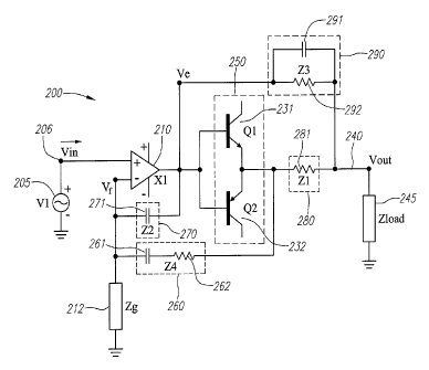
[0022] FIG. 2 is a schematic diagram of an amplifier showing, among other
things, an arrangement of impedance networks in accordance with one embodiment
as disclosed herein.
[0023] FIG. 3 is a schematic diagram of another embodiment of an amplifier
similar to that of FIG. 2, but having an additional feedback loop.
[0024] FIG. 4 is a graph showing an example of distortion performance that
can
be achieved by an amplifier built according to the principles disclosed
herein, under
certain load parameters.
[0025] FIG. 5 is a block diagram of another amplifier design using an
amplifier
cascading technique.
[0026] FIG. 6 is a block diagram illustrating another example of an
amplifier
design in accordance with various embodiments as disclosed herein.
[0027] FIG. 7a is a schematic diagram of a current limiting circuit as
known in
the prior art, while 7b is a schematic diagram of an alternative current
limiting circuit
as may be used in connection with various embodiments as disclosed herein.
[0028] FIGS. 8a and 8b are diagrams comparing the frequency responses of
different amplifier designs.
DETAILED DESCRIPTION OF PREFERRED EMBODIMENTS
[0029] According to one or more embodiments, a low power amplifier is
provided having at least a first amplifier configured as or including a driver
stage and
- 8 -
CA 02753575 2011-08-24
WO 2010/099349
PCT/US2010/025455
a second amplifier configured as or including a main output stage, biased into
operating modes in which they draw very little idle power, yet also consume
very little
dynamic power when active. A plurality of impedance networks provide, among
other things, feedback paths from the outputs of the first amplifier and the
second
amplifier to the first amplifier, enabling in part the ability of the low
amplifier to
combat distortion. The impedance networks may also provide a coupling path
from
the output of the second amplifier including the main output stage to the
load, and
another coupling path from the output of the first amplifier including the
driver stage
amplifier to the load. The impedance networks are preferably resistors,
capacitors,
or network combinations thereof.
[0030] An additional feedback path may also be provided from the load to
the
input of the first amplifier. The additional feedback path may include a low
pass filter
and more specifically a T-network of two resistors and a capacitor, and may
help
flatten out the frequency response of the amplifier at low frequencies. An
intermediate amplifier stage may also be added between the driver stage
amplifier
and the main output stage to provide additional versatility and distortion
reduction.
[0031] The first and second amplifiers are both preferably operated in low
power
dissipation modes, although in some embodiments where power dissipation is not
as
critical, one or both of the amplifiers can be operated in a higher power
dissipation
mode in order to, e.g., simplify the design, further reduce distortion (if
necessary), or
for other reasons. As used herein a low power dissipation mode or low
dissipation
mode generally includes those operating modes in which standing or idle
current
dissipation is kept low, and thus would generally include Class B, G and H
modes,
and potentially Class AB mode in certain configurations.
- 9 -
CA 02753575 2011-08-24
WO 2010/099349
PCT/US2010/025455
[0032] As one example, the first amplifier including the driver amplifier
stage
may be operated in a Class AB mode, while the second amplifier including the
main
output stage may be operated in a Class B and/or Class G or H mode. Thus, the
overall power draw of the amplifier may be kept very low. The second amplifier
may
alternatively be operated in Class AB mode at the expense of increased power
dissipation, which may lower distortion even further. As another example, both
the
first and second amplifiers can be operated in Class G mode, or both operated
in
Class H mode, or one in Class G mode and the other in Class H mode. The novel
amplifier designs disclosed and taught herein therefore provide a great deal
of
flexibility and versatility in terms of operating mode selection and overall
design
configuration. The amplifier design can be tailored for specific purposes
including
extremely low power dissipation, very low distortion, compact structure, etc.,
or
combinations thereof.
[0033] Figure 1 is a generic schematic diagram of an example of a
conventional
linear amplifier 100 as known in the prior art. As shown in Figure 1, the
linear
amplifier 100 includes an input stage 110, a driver stage 120, and an output
stage
150 that may include, for example, a pair of transistors 131 and 132 (also
labeled as
Q1 and Q2 in Figure 1) coupled to positive and negative voltage rails 130, 135
(also
labeled as +V and ¨V in Figure 1). The input stage 110, driver stage 120, and
output
stage 150 are connected in a serial arrangement. The input stage 110 receives
an
input signal 106 from an input signal source 105. The output stage transistors
Q1,
Q2 are normally biased by a voltage source 128 (also labeled Vb) into either
Class B
or Class AB operation. While shown in Figure 1 as single transistors, the
output
stage transistors Q1 and Q2 may be embodied as different types of circuit such
as
-10-
CA 02753575 2011-08-24
WO 2010/099349 PCT/US2010/025455
single transistors, compound transistor arrangements or FETs. The output stage
150 provides an amplified output signal 140 to a load 145 (represented as an
impedance in Figure 1).
[0034] Also in Figure 1, a feedback capacitor 124 (also labeled as Z2 in
Figure
1) applies local feedback around the driver stage 120 whilst ensuring
stability by
introducing a 6dB/octave roll-off to the open loop frequency response of the
amplifier
100. Driver stage 120 is typically biased into Class A operation. Input stage
110 is
typically implemented as a transconductance stage. Additional resistors 115
and
112 (also labeled as R4 and Rg in Figure 1) provide overall negative feedback
around the complete amplifier.
[0035] As mentioned earlier, an amplifier of this generic type generally
suffers
from poor idle and dynamic dissipation performance when biased into Class AB
operation, and poor distortion performance when biased into Class B operation.
Dissipation can be reduced by operating in Class G mode, but then more
distortion
mechanisms are introduced which are difficult to address by means of
conventional
negative feedback.
[0036] According to one or more embodiments disclosed herein, and as
explained for example in connection with Figure 2, distortion is significantly
reduced
over the conventional linear amplifier of Figure 1 by providing a signal path
from the
gain/driver stage X1 to the output by means of an impedance network Z3 whilst
also
introducing another impedance network Z1. Figure 2 is a schematic diagram of a
novel amplifier design in accordance with one embodiment as disclosed herein,
illustrating a useful arrangement of impedance networks and other amplifier
circuitry
by way of one example. In Figure 2, an amplifier 200 includes, among other
things,
-11 -
CA 02753575 2011-08-24
WO 2010/099349 PCT/US2010/025455
a gain/driver stage 210 (also labeled as X1 in Figure 2) and an output stage
250 that
may include, for example, a pair of transistors 231 and 232 (also labeled as
Q1 and
Q2 in Figure 2) coupled, similar to Figure 1, to positive and negative voltage
rails +V
and -V (not shown in Figure 2). The gain/driver stage 210 receives an input
signal
206 from an input signal source 205. While shown in Figure 2 as single
transistors,
as with Figure 1 and all other embodiments that will be described herein, the
output
stage transistors Q1 and Q2 may be embodied as different types of circuit such
as
single transistors, compound transistor arrangements or FETs. The output stage
250 provides an amplified output signal 240 to a load 245 (represented as an
impedance in Figure 2).
[0037] More generally, the gain/stage 210, while conceptually shown as a
single
amplifier in Figure 2, may be constructed from multiple amplifier stages or
may be
included as part of a larger amplifier block. Likewise, the output stage 250,
while
shown as primarily consisting of transistors Q1 and Q2, may be included as
part of a
larger amplifier block which may contain one or more stages, and would also be
understood to include bias components, protection elements, and other
conventional
features that are not shown in detail in Figure 2 for the sake of simplicity.
Those
skilled in the art will appreciate that there are many different ways to
implement the
gain/driver stage 210 and output stage 250 of amplifier 200.
[0038] As noted above, an impedance network 290 (also labeled as Z3 in
Figure
2) is provided between the output of the gain/driver stage 210 and the load
245.
Another impedance network 280 (also labeled as Z1 in Figure 2) is provided
between the output stage 250 and the load 240. Another impedance network 270
(also labeled as Z2 in Figure 2) is provided from the output of the
gain/driver stage
- 12-
CA 02753575 2011-08-24
WO 2010/099349
PCT/US2010/025455
210 to one of the differential inputs of the gain/driver stage 210. A fourth
impedance
network 260 (also labeled as Z4 in Figure 2) is provided from the output stage
250 to
the same differential input of the gain/driver stage 210. Impedance networks
260
and 270 are coupled to ground (or some other reference potential) by another
impedance network 212 (also labeled as Zg in Figure 2).
[0039] In the example of Figure 2, impedance network 290 is embodied as a
capacitor 291 and resistor 292 connected in parallel. Impedance network 280 is
embodied as a resistor 281. Impedance network 270 is also embodied as a
resistor
271. Impedance network 260 is embodied as a resistor 262 and capacitor 261
connected in series.
[0040] Choosing the values of the impedance networks Z1, Z2, Z3, Z4 such
that
they satisfy the relationship Z1(s)-Z2(s) = Z3(s)-Z4(s), the distortion on the
amplifier
200 can be significantly reduced compared to a standard feedback amplifier of
the
type shown in Figure 1. As noted above, in this example impedance network Z1
is
preferably embodied as a resistor, impedance network Z2 is preferably embodied
as
a capacitor, impedance network Z3 is preferably embodied as a parallel
combination
of resistor and capacitor, and impedance network Z4 is preferably embodied as
a
series combination of resistor and capacitor, although other equivalent
impedance
networks may be used. The time constant of the impedance network Z3 preferably
matches that of impedance network Z4. At low frequencies, below the frequency
at
which the impedance of Z3 become capacitive, impedance network Z3 appears
resistive in nature and impedance network Z4 appears to be capacitive. The
presence of impedance network Z3 softens the crossover knee of the output
stage
-13-
CA 02753575 2011-08-24
WO 2010/099349 PCT/US2010/025455
250 by virtue of the driver stage to load output connection through impedance
network Z3.
[0041] In order to gain maximum distortion reduction, impedance network Z4
is
preferably capacitive in nature so that the ratio of impedances of Z2:Z4
equals
Z3:Z1. However, this means that the open loop gain of the feedback loop around
the
output stage 250 no longer falls off with frequency. Incorporating a series
resistor
within Z4 reinstates the fall in gain with frequency above the breakpoint at
which Z4
stops appearing capacitive and becomes resistive in nature. The resistor 262
in
impedance network Z4 is chosen to set a unity loop gain frequency that ensures
stability.
[0042] To retain full distortion reduction, impedance network Z3 should be
made
to appear capacitive in nature at high frequencies; hence the matching of the
time
constants of impedance networks Z3 and Z4. There is generally a free choice of
time constant for the components of impedance networks Z3 and Z4. However, the
larger the time constant, the larger the capacitor has to be in impedance
network Z3,
and the greater the current that will be drawn from the gain/driver stage 210
(i.e., X1)
at high frequencies. To minimize size of the amplifier 200, the time constant
for
impedance networks Z3 and Z4 should be kept low.
[0043] The balancing of the impedance networks will work even in the
presence
of parasitic elements in the impedance networks. For instance, a parasitic
inductance in series with resistor 281 can be balanced by placing a suitable
value
resistor in series with capacitor 291. As reflected by the example of Figure
2, all of
the components of impedance networks Z1 ¨ Z4 can be realized as resistors,
capacitors or combinations thereof (excluding parasitic elements). This design
- 14 -
CA 02753575 2011-08-24
WO 2010/099349
PCT/US2010/025455
approach can lead to a very compact amplifier package. The term "resistor" in
this
context includes any resistive element that displays a substantially constant
impedance relationship over the applicable operating frequency range, and will
typically, but not necessarily, involve a conventional discrete resistor
component.
[0044] By itself, the choice and arrangement of impedance networks in
Figure 2
works adequately but can be improved. For example, the incorporation of the
series
capacitor 262 within impedance network Z4 means that below the break frequency
formed by its series resistor/ capacitor combination of elements 261 and 262,
the
closed loop gain of the complete amplifier 200 increases at 6dB/octave as
frequency
decreases. Additionally, the open loop gain around transistors Q1, Q2 due to
the
arrangement of impedance networks Z2 and Z4 and gain/driver stage 210 becomes
constant at low frequencies rather than rising at 6dB/octave with decreasing
frequency as with a conventional feedback amplifier. Thus, the distortion
reduction
around transistors Q1 and Q2 by means of negative feedback will be lowered as
compared to a conventional amplifier with this choice of impedance networks.
Additional distortion reduction will still be achieved by virtue of the
incorporation of
impedance network Z3 into the amplifier 20, but there is still room for
improvement,
as will be explained in more detail below. Also, the output resistance of the
amplifier
200 is approximately equal to the parallel combination of the impedance
networks Z1
and Z3. In the case where the first impedance network Z1 is embodied as a
resistor,
the output resistance of the amplifier 200 at low frequencies is generally
higher than
would be the case for a purely conventional feedback amplifier such as
illustrated in
Figure 1.
- 15-
CA 02753575 2011-08-24
WO 2010/099349 PCT/US2010/025455
[0045] Figure 3 illustrates how further improvements can be made to
distortion
performance and closed loop response in the foundational amplifier design of
Figure
2. In Figure 3, elements labeled 3xx generally correspond to the similar
elements
labeled 2xx in Figure 2. In Figure 3, an amplifier 300 receives an input
signal 306
from an input signal source 305. Similar to the amplifier 200 of Figure 2, the
amplifier 300 of Figure 3 includes a gain/driver stage 310, an output stage
350
comprising transistors 331 and 332 (also labeled as Q1 and Q2), and impedance
networks 360, 370, 380 and 390 (also respectively labeled as Z4, Z2, Z1 and Z3
in
Figure 3). A network 356 comprising resistors 352, 353 (also labeled as R5, R6
in
Figure 3) and a capacitor 354 (also labeled as C7 in Figure 3) has been added
to the
amplifier 300 to form an additional feedback loop. The feedback is taken from
the
final output 340 of the amplifier 300 rather than the output stage 350
directly
although it is then fed into the same feedback input terminal of gain/driver
stage 310
as the existing feedback loop that is based upon impedance networks Z2 and Z4.
Notwithstanding this, this connection of the extra feedback loop does not
upset the
conditions required for maximum distortion reduction.
[0046] Simply adding another resistive feedback path to the amplifier
arrangement of Figure 2 would generally result in a non-flat frequency
response
because extra feedback loop is placed around the closed loop system of Figure
2,
and the closed loop gain is not large enough to ensure that the final closed
loop
response of the amplifier is independent of the value of the Figure 2 closed
loop
gain. However, by designing the extra feedback network 356 to have a low pass
filter response with a cut-off frequency that matches the breakpoint frequency
of
impedance networks Z3 and Z4 and with an appropriate gain, then the overall
- 16-
CA 02753575 2011-08-24
WO 2010/099349
PCT/US2010/025455
amplifier 300 can be designed to have a flat response. Thus the rising low
frequency
response of the amplifier system of Figure 2 is perfectly compensated by the
design
additions of Figure 3.
[0047] The extra feedback loop of Figure 3 provided by the addition of
feedback
network 356 also additionally reduces distortion at low frequencies,
compensating for
the compromised low frequency distortion performance of the Figure 2 amplifier
implementation. Furthermore, this extra feedback loop also reduces the output
impedance of the amplifier at low frequencies since the feedback is taken from
directly across the load 345 and hence impedance network Z1 is within this
feedback
loop.
[0048] Having the extra overall frequency dependent feedback loop to lower
the
output impedance of the amplifier 300 allows the bridge impedance network Z1
to
have a higher impedance than would otherwise be possible, within the
constraints of
power losses within the resistor 381 of the impedance network Z1; thus, the
impedance of element Z3 can be similarly increased to lower the value of the
parallel
capacitance and with it the high frequency current that must be sourced from
the
gain/driver stage 310.
[0049] The available choices of capacitor and resistor values for impedance
networks Z1-Z4 means that balancing at high frequency ranges can be more
accurately attained, since capacitors and resistors of the values used for the
amplifier design of Figure 3 can be readily obtained with close manufacturing
tolerances. The voltage that appears across the capacitor 391 within impedance
network Z3 is quite small (it is only the gain/error loss in the output stage
plus the
product of the output current times the impedance of Z1) and so its package
size,
- 17-
CA 02753575 2011-08-24
WO 2010/099349
PCT/US2010/025455
given the low voltage requirements of the capacitor 391, is also
commensurately
small, allowing for miniaturization of the amplifier 300. Multiple amplifiers
using the
design shown in Figure 3 can be placed in close proximity with little
interaction
between the impedance networks, because the lack of balancing inductors means
that there is less possibility of magnetic coupling among the amplifiers.
[0050] The use of the additional impedance networks Z1, Z3 and Z4 and the
extra feedback loop provided by the addition of feedback network 356 allows
the
high frequency distortion of the amplifier 300 to be significantly lower than
a
conventional feedback amplifier and so the output stage 350 could potentially
be
operated, for example, in Class B mode whilst still avoiding crossover
distortion.
Thus, idle power dissipation that normally occurs due to the quiescent current
required to bias a conventional amplifier output stage into Class AB mode is
eliminated by the design of Figure 3. This might be of limited use if the
gain/driver
stage 310 of amplifier 300 were required to have a high idle current drain.
However,
the gain/driver stage 310 in this example operates at much lower power than
the
main output stage 350 based around transistors Q1 and Q2, and so the
gain/driver
stage 310 can be configured with a Class AB output stage 350 having linear,
fast
output devices (transistors Q1 and Q2) and so still operate with low
distortion
compared to the main output stage 350. Thus the dissipation in the gain/driver
stage
310 can also be very low.
[0051] By incorporating a low power Class AB output stage internally within
the
gain/driver stage 310, the distortion introduced into the error signal by the
Class AB
operation of the gain/driver stage 310 can be made exceedingly small.
Typically, for
an audio power amplifier according to the design shown in Figure 3 capable of
- 18 -
CA 02753575 2013-04-25
delivering 100 Watts nominal output power into a 16 ohm load, the gain/driver
stage
310 can be configured to operate for instance with only 1-2 milliamps of
quiescent
current, which is quite low.
[0052] Given the significant reduction in high frequency distortion of the
output
stage 350, the dynamic power dissipation of the amplifier 300 can also be
reduced by
employing a Class G or Class H architecture. Unlike with a conventional
feedback
amplifier, the high frequency distortion components introduced by the Class G
rail
switching transitions or Class H tracking scheme will be reduced by using the
amplifier feedback configurations of some of the embodiments disclosed herein
so
that a very low distortion, very low idle power dissipation, low dynamic power
dissipation amplifier can be realized. One example of a tracking power supply
that
can be used in conjunction with the amplifier designs disclosed herein to
provide
additional power savings is described in United States Patent No. 7,834,702.
The use
of a Class G or H architecture for the first amplifier containing the
gain/input stage
may have the potential to introduce non-linearities into the system, which
could need
to be controlled or otherwise taken account of.
[0053] Where a Class G or H architecture is applied to both the first and
second
amplifiers, different power rails (with different voltage levels) may be
provided to the
first amplifier and the second amplifier to, e.g., help isolation, reduce non-
linearities,
and minimize power dissipation.
[0054] Figure 4 shows an example of the distortion performance that can be
achieved by an amplifier built according to the principles outlined above,
when
-19-
CA 02753575 2011-08-24
WO 2010/099349
PCT/US2010/025455
capable of driving a 56 Volt peak signal into a 16 ohm load using an amplifier
design
constructed according to Figure 3. As shown in Figure 4, the total harmonic
distortion is quite low at relatively low frequencies (generally ranging from
about
0.0003 to 0.0010 percent distortion level at 1 kHz), and remains low even at
higher
frequencies (generally ranging from about 0.0020 to 0.0050 percent distortion
level
at 10 kHz).
[0055] Figures 8a and 8b are idealized frequency response graphs showing
the
effect of the additional feedback loop 356 in the embodiment of Figure 3.
Figure 8a
shows that at relatively low frequencies, the overall amplifier gain drops
off, then
flattens out at a shelf region, and then later drops off again with increasing
frequency. By using the additional feedback loop of Figure 3, this frequency
response can be altered as shown in Figure 8b. The low frequency response is
perfectly compensated by the outer feedback loop, resulting in a flat
frequency
response out to relatively high frequencies. The outer frequency loop can also
be
used for additional purposes, such as to extend the operating range of the
amplifier
through the introduction of an additional zero and pole at high frequencies.
[0056] Further modifications or enhancements can also be made to the
amplifier
architectures described above. For example, although the distortion of the
Class AB
gain/driver stage 310 can be made to be low compared to that of the output
stage
350, it will still generate some residual distortion. To overcome this, the
Class AB
gain/driver stage 310 can itself employ the same distortion reduction
technique as
used around the output stage 250 as previously outlined in connection with
Figure 2.
[0057] This "cascaded" approach is illustrated in the amplifier design
shown in
Figure 5. Elements in Figure 5 labeled "5xx" generally correspond to the
similar
-20-
CA 02753575 2011-08-24
WO 2010/099349
PCT/US2010/025455
elements labeled "3xx" in Figure 3. In Figure 5, an amplifier 500 receives an
input
signal 506 from an input signal source 505. Similar to the design of Figure 3,
the
amplifier 500 includes a gain/driver stage 510, an output stage 550 comprising
transistors 531 and 532 (also labeled as Q1 and Q2), and impedance networks
560,
570, 580 and 590 (also respectively labeled as Z4, Z2, Z1 and Z3 in Figure 5).
An
additional feedback network 556 comprising resistors 552, 553 (also labeled as
R5,
R6 in Figure 5) and a capacitor 554 (also labeled as C7 in Figure 5) is
included in the
amplifier 500, having the same general purpose as in Figure 3, with feedback
being
taken from the final output 540 of the amplifier 500 and fed into the feedback
input
terminal of gain/driver stage 350. Also added in Figure 5 is an intermediate
stage
542, which in one aspect may act as a second or supplemental driver stage,
comprising transistors 543 and 544 (also labeled as Q3 and Q4) and voltage
bias
components 546 and 547. The transistors 543 and 544 and coupled to the
positive
voltage rail +V and negative voltage rail ¨V respectively, and may be biased
into
Class AB operating mode by bias components 546 and 547
[0058] The output of the intermediate stage 542 is coupled to the input of
the
output stage 550 via a resistor 529 (also labeled as Z1i in Figure 5). An
additional
resistor 528 (also labeled as Z3i) is connected from the input of the output
stage 550
to the input of the intermediate stage 542. The feedback taken from impedance
network 590 (Z3) thus passes through resistor 528 for purposes of intermediate
stage 542, although it is still applied directly to the input of the output
stage 550. An
additional capacitor 548 (also labeled Z2i in Figure 5) is provided from the
output of
the gain/driver stage 510 to the feedback input terminal thereof. The feedback
derived from impedance network 570 (Z2) is taken from the output of the
- 21 -
CA 02753575 2011-08-24
WO 2010/099349
PCT/US2010/025455
intermediate stage 542 instead of the output of the gain/driver stage 510. The
additional elements 529, 548 and 528 (Zli, Z2i and Z3i) form part of an inner
feedback loop, while impedance network 570 (Z2) shares its operation between
the
inner and outer feedback loops.
[0059] Both the gain/driver stage 510 and the intermediate stage 542
provide
some aspect of feed-forward operation, in that both provide current to the
load when
the main output stage 550 is relatively idle, and hence both may be viewed as
having
a driver function to some degree. Both stages may also supply gain. In this
respect,
the designation of particular stages as "gain" or "driver" stages is not
intended to be
limiting.
[0060] In the example shown in Figure 5, the inner loop components 529, 548
and 528 (Z1i, Z2i and Z3i) have been chosen, along with impedance network 570
(Z2), such that the inner loop realizes the distortion reduction condition
described for
the Figure 3 amplifier design, with the Class AB stage (i.e., the internal
output stage
of gain/drive stage 510, in certain embodiments) retaining an integrator type
response in respect of the action seen by the outer loop. A resistor 572 (R2)
has
been added to impedance network 570 (Z2) to help ensure stability of the inner
feedback loop around transistors Q3 and Q4, while another resistor 592 (R3i)
has
been added to impedance network 590 (Z3) to compensate the outer feedback loop
for the zero introduced into the integrator response by resistor 572. This
arrangement makes it possible for the other outer loop components of impedance
networks Z1 - Z4 to remain the same as the example illustrated in Figure 3.
The
retention of the high frequency roll-off of the improved driver stage
comprising
gain/driver stage 510 and intermediate stage 542 allows stability of the
feedback
- 22 -
CA 02753575 2011-08-24
WO 2010/099349
PCT/US2010/025455
loop around the output stage 550, and the final overall feedback loop still
allows for
low output impedance of the amplifier 500 at audio frequencies.
[0061] Other arrangements of the inner loop impedance networks are also
possible. For example, if an extra gain stage is introduced before gain/driver
stage
510, then capacitor 571 (C2) in impedance network 570 (Z2) could be dispensed
with and resistor 528 (Z3i) replaced with a capacitor. The gain of this inner
loop
would then be flat with frequency, so the extra gain stage could be given an
integrator response and the outer bridge and loop components Z4, R5, R6, C7,
Zg
could be connected to the input of the additional integrator gain stage.
[0062] Such an arrangement is detailed in Figure 6. Elements in Figure 6
labeled "6xx" generally correspond to the similar elements labeled "5xx" in
Figure 5.
In Figure 6, an amplifier 600 receives an input signal 606 from an input
signal source
605. Similar to Figure 5, the amplifier 600 includes a gain/driver stage 610B,
an
intermediate stage 642 comprising transistors 643 and 644 (also labeled as Q3
and
Q4) and voltage bias components 646 and 647, and an output stage 650
comprising
transistors 631 and 632 (also labeled as Q1 and Q2), along with impedance
networks 660, 670, 680 and 690 (also respectively labeled as Z4, Z2, Z1 and Z3
in
Figure 6). An additional gain stage 610A (also labeled X2 in Figure 6) has
been
added before the gain/driver stage 610B. The amplifier 600 further includes an
outer
feedback network 656 comprising resistors 652, 653 (labeled as R5, R6) and
capacitor 654 (labeled as C7), having a similar purpose as in Figures 3 and 5,
with
feedback being taken from the final output 640 of the amplifier 600 and fed
into a
feedback input terminal of gain stage 610A. In this case, the impedance
network
670 (Z2) is positioned between the output of the gain stage 610A and the
feedback
- 23 -
CA 02753575 2011-08-24
WO 2010/099349
PCT/US2010/025455
input terminal of gain stage 610A. Similarly, the impedance network 660 (Z4)
is
positioned between the output of the driver stage 650 and the feedback input
terminal of gain stage 610A.
[0063] The feedback from the output of gain/driver stage 610B continues to
run
through capacitor 648 (Z2i) into the feedback input terminal of the
gain/driver stage
610B. A feedback connection is also made from the output of the intermediate
stage
642 to the feedback input terminal of the gain/driver stage 610B. In this
case, the
feedback element is a resistor 619 (also labeled as R2), and another resistor
618
(also labeled Rgi) has been added coupling the feedback input terminal of the
gain/driver stage 610B to ground (or some other reference potential).
Capacitor 628
and resistor 629 (also labeled as Z3i and Zli respectively) perform similar
functions
to their counterparts in Figure 5, both of them forming part of the inner
feedback
loop.
[0064] In the design of Figure 6, the added gain stage 610A is configured
with
an integrator response (using the capacitor 671 of impedance network Z2), and
the
outer bridge and loop components Z4, R5, R6, C7, Zg are connected to the
feedback
input of the added gain stage 610A instead of the gain/driver stage 610B. The
gain
of the inner feedback loop including resistors 618 and 619 (Rgi and R2) is
flat with
frequency.
[0065] As with Figure 5, in the example of Figure 6 the other inner loop
components 629, 648 and 628 (Z1i, Z2i and Z3i) have been chosen, along with
impedance network 670 (Z2), such that the inner loop realizes the distortion
reduction condition described for the Figure 3 amplifier design, with the
Class AB
stage (i.e., the internal output stage of gain/drive stage 510, in some
embodiments)
- 24 -
CA 02753575 2011-08-24
WO 2010/099349
PCT/US2010/025455
retaining an integrator type response in respect of the action seen by the
outer loop.
The choice of outer loop impedance network values to ensure maximum distortion
reduction now has to take account of the gain of the inner loop which
increases the
effective impedance of Z2 by the ratio [R2+Rgi]/Rgi. A resistor in impedance
network 670 (Z2) is not needed for stability of the inner feedback loop around
transistors Q3 and Q4. This arrangement again makes it possible for the other
outer
loop components of impedance networks Z1-Z4 of the Figure 3 amplifier design
to
remain the same. The retention of the high frequency roll-off of the inner
amplifier
subsystem comprising gain stage 610A, gain/driver stage 610B, and intermediate
stage 642 allows stability of the feedback loop around the output stage 650,
and the
final overall feedback loop still allows for low output impedance of the
amplifier 600
at audio frequencies.
[0066] If the output impedance of the inner amplifier subsystem is an
appreciable value in comparison to the impedance of Z3, then impedance network
Z3 can be modified (i.e., increased) to ensure correct distortion reduction.
[0067] By utilizing these extra network arrangements in the amplifier
designs of
Figures 5 and 6, the dissipation of the Class AB driver stage (that is, the
internal
output stage of the gain/driver stage 510 or 610B, in some embodiments) can be
made even lower by reducing the Class AB quiescent current further, since its
distortion can be greatly reduced by the techniques described. The Class AB
stage
of the gain/driver stage 510 or 610B could itself be biased in Class B,
resulting in a
reduction of idle dissipation.
[0068] A further reduction in idle dissipation can be obtained by operating
the
gain/driver stage 210, 310, 510 or 610B in Class G or H mode, since the
quiescent
- 25 -
CA 02753575 2011-08-24
WO 2010/099349
PCT/US2010/025455
power supply voltage to the gain/driver stage will be lower than would be the
case
otherwise. This could be done also without the extra network(s) of Figure 5 or
6, but
extra care would be needed in order to eliminate any power supply switching
spikes
from affecting the output of the gain/driver stage. The extra network
circuitry allows
any switching distortion introduced into the gain/driver stage to be
significantly
reduced.
[0069] Amplifiers generally incorporate small current sensing resistors in
series
with the output transistors in order to provide for current limiting
protection circuits.
Impedance network Z1 employed in the various amplifier designs of Figures 2,
3, 5
and 6 can be used to replace these current sensing resistors as depicted in
Figures
7a and 7b. Figure 7a shows a conventional current limiting circuit arrangement
in
which a push-pull output stage 700 comprises n-type transistor 711 and p-type
transistor 712 (also labeled as Q1 and Q2) that are inter-connected with a
combination of circuitry including transistors 721, 722 and 723 (also labeled
as Q3,
Q4 and Q5 respectively), current source 724 (also labeled as II), and
resistors 714
and 715 through which the output signal passes to reach the final output 720
of the
output stage 700. The amount of current that can be output from transistor 711
is
limited by the current that passes through resistor 714, and that amount of
current is
in turn determined by the base-to-emitter voltage of transistor 721. Resistor
715 and
transistor 722 operate in a similar fashion to protect transistor 712 from
excessive
output current.
[0070] Figure 7b, on the other hand, shows a modified current limiting
circuit
arrangement that takes advantage of the presence of impedance network Z1 to
dispense with resistors 714 and 715. In Figure 7b, output stage 750 comprises
n-
- 26 -
CA 02753575 2011-08-24
WO 2010/099349
PCT/US2010/025455
type transistor 731 and p-type transistor 732 (also labeled as Q1 and Q2) that
are
again inter-connected with a combination of circuitry including transistors
751, 752
and 753 (also labeled as Q3, Q4 and Q5 respectively), current source 754 (also
labeled as 11), and, in this case, resistor 781 which may be the resistor in
impedance
network Z1 of any of the previous embodiments described herein. In this case,
when
transistor 731 (Q1) is ON, then resistor 781 serves to limit the output
current in the
same way as resistor 714, i.e., using the relatively fixed base-to-emitter
voltage of n-
type transistor 751 to limit the output current, and when transistor 732 (Q2)
is ON,
then resistor 781 limits the output current in the same way as resistor 715,
i.e., using
the relatively fixed emitter-to-base voltage of p-type transistor 752 to limit
output
current.
[0071] The invention has generally been illustrated or discussed with
particular
reference to an audio power amplifier but is by no means limited to this
application
area. The disclosed techniques apply also, for example, to low power audio
amplifiers, video amplifiers and radio frequency amplifiers, among others.
[0072] According to various embodiments as disclosed herein, a power
amplifier
is provided having low power dissipation and, more specifically, is capable of
having
low idle and dynamic power dissipation levels. The power amplifier may not
require
a bias setting, and further may not require inductors for EMI or filtering.
The power
amplifier may also deliver very low distortion levels.
[0073] In certain embodiments described herein, a low-power, low-distortion
amplifier includes a gain/driver stage, an optional intermediate stage, and an
output
stage in a cascaded arrangement. A coupling path, which may in one aspect be
viewed as a feed-forward path, is provided from the output of the gain/driver
stage to
- 27 -
CA 02753575 2011-08-24
WO 2010/099349
PCT/US2010/025455
the load, via a feed-forward impedance network that may include a capacitor
and a
resistor connected in parallel. The output stage may be coupled to the load by
another impedance network such as a resistor. The output stage may also be
coupled to the input of the gain/driver stage by another impedance network,
which
may take the form of a capacitor and a resistor in a series arrangement. The
output
of the gain/driver stage may also be coupled to its input by another impedance
network, which may take the form of a capacitor.
[0074] In addition, a feedback network may be provided from the load to the
input of the gain/driver stage for stabilization, which may have the affect of
flattening
the overall frequency response at low frequencies will leaving the response
unchanged at higher frequencies. The additional feedback network may take the
form of a low pass filter and, more specifically, a T-network of two series
resistors
and a capacitor connected between their common node and a reference potential
(such as ground). The additional feedback network may be used to counter-act
the
resistive nature of the frequency response of the feed-forward impedance
network at
low frequencies. Because the additional feedback network is fed into the
negative
input of the gain/driver stage, it effectively cancels out the low frequency
component
of the amplifier's frequency response contributed by the feed-forward
impedance
network.
[0075] In some embodiments, an additional intermediate amplifier stage may
be
provided, which functions in certain respects as a driver stage, and has a
feed-
forward path coupling to the load via the third impedance element.
[0076] In certain embodiments, the main output stage is operated in Class B
mode, while the gain/driver stage is operated in Class AB mode, thus leading
to a
- 28 -
CA 02753575 2011-08-24
WO 2010/099349
PCT/US2010/025455
low power dissipation configuration. At low signal levels, the gain/driver
stage
(and/or an intermediate amplifier stage) may provide the drive for the output
signal
via the feed-forward or coupling between the gain/driver stage (and/or the
intermediate amplifier stage) and the load, (through impedance network Z3,
while at
higher signal levels the main output stage drives the load. In alternative
embodiments, one or both of the gain/driver stage and the main output stage
may be
operated in Class G or H mode, with the addition of an appropriate power
supply for
the amplifier. In alternative embodiments, the main output stage may be
operated in
Class AB mode, or else in Class A mode. While doing so may increase power
dissipation, this configuration may still take advantage of other benefits
provided by
the novel designs discussed herein.
[0077] The novel power amplifier embodiments of Figures 2, 3, 5 and 6 may
be
realized in a very small package and, in particular, may be implemented
entirely on a
single chip, with the possible exception of the capacitive component of
impedance
network Z3 which may, in some cases, be large but still relatively small as
compared
to an inductor, hence allowing smaller overall packaging size. Because of the
amplifier's low power dissipation, multiple amplifiers (such as four, eight,
or possibly
more) may be included on a single chip without the risk of over-heating. Such
a chip
can be particularly convenient for multi-channel amplifier system such as used
in
audio applications or for other purposes.
[0078] As noted above, the amplifier designs disclosed herein may be
suitable
for many different types of applications, including audio or sound
reproduction,
communications, satellites, and other applications. The novel amplifier
designs can
potentially have very wide frequency range with substantially flat or constant
gain,
- 29 -
CA 02753575 2013-04-25
while maintaining low power dissipation and low distortion. For example, the
amplifier
may provide relatively flat or constant gain over the range of 20 Hz to 20 KHz
for
audio applications, but is not so limited, and conceptually may provide flat
or constant
gain over a much larger pass-band, depending upon the specific application.
[0079] While preferred embodiments of the invention have been described
herein,
many variations are possible which remain within the concept and scope of the
invention. Such variations would become clear to one of ordinary skill in the
art after
inspection of the specification and the drawings. The invention therefore is
not to be
restricted except within the scope of any appended claims.
- 30 -