Note: Descriptions are shown in the official language in which they were submitted.
CA 02753680 2011-08-25
WO 2010/111362 PCT/US2010/028461
APPARATUS AND METHOD FOR DETERMINING A TOUCIi INPUT
[0001] This application claims priority from provisional U.S. Application No.
61/163,237 filed March 25, 2009, and entitled "Time Domain Differential
Sensing."
FIELD OF THE INVENTION
[00021 The present invention relates to an apparatus and method for sensing a
touch input on a touch surface, and more particularly, to an electronic
circuit and method
for detecting a touch input.
BACKGROUND OF THE INVENTION
[00031 Touch inputs on a touch surface are widely used as an input
methodology.
Touch inputs may be best known in conjunction with appliance control panels,
smart
phones and other handheld devices. However, touch screens and touch inputs are
gaining
widespread acceptance as a user interface over a wide variety of applications.
It is also
important that a touch surface have an appropriate sensitivity to touch. If
the surface is
"too sensitive," it may be susceptible to noise, or it may register false
touches. If the
surface is "too insensitive," it may not accurately register desired touches,
or fail to
register a touch altogether.
[00041 Capacitance sensing has been well established as a method of detecting
a
variety of stimuli, including touch inputs, with an improved sensitivity to
touch.
Capacitive sensors normally require at least one electrical element typically
referred to as
an electrode, element, or plate. In some instances, there may be one, two or
more
networks of capacitive electrodes, elements or plates. These elements are
geometrically
-1-
CA 02753680 2011-08-25
WO 2010/111362 PCT/US2010/028461
designed to cause the formation of a net electric field in both a non-stimulus
state as well
as a stimulus state.
[00051 Many methods of generating an output based on the difference between a
non-stimulus state and a stimulus state are known in the art. According to one
known
method, a capacitive sensor is provided which includes at least one electrode.
The
electrode can be geometrically designed to detect a change in capacitance due
to a
stimulus, e.g., the presence of a nearby object. A measuring circuit converts
the output of
the electrode into a voltage, current, frequency, period or pulse width that
is linearly or
non-linearly proportional to the change in capacitance of the electrode. The
electronic
measuring circuit then evaluates the change in capacitance against a
predetermined
reference value. A change in capacitance in excess of the predetermined
reference value
indicates the proximity of the object to the capacitive sensor.
[00061 Problems with the aforementioned method include: (1) inability to
compensate for dielectric variations among different objects; (2)
susceptibility to
environmental conditions; (3) inability to compensate for manufacturing
tolerances and
variations in component materials; and (4) when configured as a touch sensor,
inability to
detect an input at the touch surface without respect to whether a finger is
gloved or not.
In an attempt to overcome the aforementioned problems, known measuring
circuits
typically average the capacitive output over a variety of non-stimulus
conditions to
achieve a desired reference value. The resulting reference value can then be
used to
determine if there is sufficient proportional change (as described above) to
indicate the
presence of a valid stimulus. However, the determination of an averaged or
compensated
reference value often requires processing in software or a devoted
microcontroller, which
2-
CA 02753680 2011-08-25
WO 2010/111362 PCT/US2010/028461
in turn can add cost and unneeded complexity to the overall system. Even with
averaging
algorithms, some variation, such as increased touch substrate thickness, can
not be
adequately compensated for to eliminate sensitivity variations.
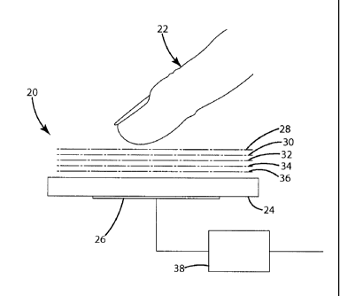
[00071 For example, consider a capacitive sensor 20 provided to sense a human
finger 22 against a given substrate 24 as shown in Fig. 1. As the finger 22 is
brought
towards the substrate 24, it approaches an electrode 26 with varying degrees
of proximity
28, 30, 32, 34, 36. Once the finger 22 has approached and moved to a first
distance 28,
the electrode 26 and the corresponding measurement circuit 38 will attempt to
detect the
stimulus as described above with an output that is proportional to the
stimulus. At this
first distance, the finger is effectively far enough from the electrode 26
that there is
effectively no stimulus condition. As the finger 22 approaches the substrate,
however,
the measurement circuit 38 evaluates the degree of stimulus against the
predetermined
reference value to determine the presence or absence of a valid stimulus. To
account for
variations in the environment, several reference values can be set to best
identify a valid
stimulus event. However, such a system would have to account for a number of
factors,
including the composition and variation of the construction materials, the
variances in
thickness of the different materials, the manufacturing processes and
variances of the
bonding of these materials, the dimensional tolerances of the electrode(s)
dimensions,
and the sensitivity preferences of the user. Alternatively, prior art systems
can average
the capacitive output over a variety of non-stimulus conditions to achieve a
single,
compensated reference value. However, the determination of a compensated
reference
value can be costly and impractical, requiring processing in software or a
devoted
microcontroller, and potentially delaying the response time of the associated
capacitive
-3-
CA 02753680 2011-08-25
WO 2010/111362 PCT/US2010/028461
sensor, and ultimately may not be able overcome sensitivity variations or
detect valid
stimuli such as a gloved or ungloved finger when the capacitive sensor is
configured as a
touch sensor.
SUMMARY OF TIIE INVENTION
[0008] The aforementioned problems are overcome by the present invention in
which a touch input is determined by monitoring the rate of change of the
position of a
stimulus, such as a finger, with respect to a touch surface. A touch is
determined when
the rate of change falls below a minimum, presumably when the stimulus engages
the
surface.
[0009] In the disclosed embodiment, the apparatus includes a capacitive sensor
having an electrode and a processing unit electrically coupled to the
electrode and
configured to determine the presence of a stimulus based on the rate of change
of the
electrode capacitance. The apparatus can further include a substrate adjacent
the
electrode, wherein the stimulus corresponds to the placement of an object
against or near
the substrate. The processing unit is configured to determine the presence of
a stimulus
in response to the rate of change of the electrode capacitance being less than
a first
predetermined value, and in response to the absolute value of the electrode
capacitance
being greater than a second predetermined value.
[0010] In another aspect of the invention, a method for detecting a stimulus
is
provided. The method includes providing a capacitive sensor, the capacitive
sensor
including an output, measuring a rate of change of the capacitive sensor
output, and
determining the presence of a stimulus based on the rate of change of the
capacitive
sensor output. The method further includes determining an object has come to
rest with
-4-
CA 02753680 2011-08-25
WO 2010/111362 PCT/US2010/028461
respect to the capacitive sensor based on the rate of change of the capacitive
sensor being
less than a first reference value. The measuring step includes detecting, over
successive
sampling intervals, a variation in the capacitive sensor output, and the
stimulus can
correspond to a metal sensor (e.g., an RPM sensor) adjacent the capacitive
sensor or the
placement of an object against a substrate overlying the capacitive sensor.
[0011] These and other features and advantages of the present invention will
become apparent from the following description of the invention, when viewed
in
accordance with the accompanying drawings and appended claims.
BRIEF DESCRIPTION OF THE DRAWINGS
[0012] Fig. I is a representation of a capacitive sensor and an associated
measurement circuit.
[0013] Fig. 2 is flow chart showing the control flow an embodiment of the
present
invention.
[0014] Fig. 3A-3B are functional block diagrams of a measurement and timing
interface circuit in accordance with an embodiment of the present invention.
[0015] Fig. 4 is a circuit diagram of the capacitive sensor 102 of the
measurement
circuit of Fig. 3A.
[0016] Fig. 5 is a circuit diagram of the stimulus detect circuit 104 of the
measurement circuit of Fig. 3A.
[0017] Fig. 6 is a circuit diagram of the input latching buffer 106 of the
measurement circuit of Fig. 3A.
[0018] Fig. 7 is a circuit diagram of the first time domain differential
latching
buffer 108 of the measurement circuit of Fig. 3A.
-5-
CA 02753680 2011-08-25
WO 2010/111362 PCT/US2010/028461
[0019] Fig. 8 is a is a circuit diagram of the second time domain differential
latching buffer 110 of the measurement circuit of Fig. 3A.
[0020] Fig. 9 is a circuit diagram of the threshold latching buffer 112 of the
measurement circuit of Fig. 3A.
[0021] Fig. 10 is a timing diagram for the measurement circuit of Fig. 3A.
[0022] Fig. 11 is a voltage versus time graph illustrating the Input Latch and
Stimulus Rate of the measurement circuit of Fig. 3A.
[0023] Fig. 12 is a voltage versus time graph illustrating the time
differential
output of the measurement circuit of Fig. 3A.
[0024] Fig. 13 is a voltage versus time graph illustrating the outputs of the
measurement circuit of Fig. 3A.
DETAILED DESCRIPTION OF THE CURRENT EMBODIMENT
[0025] The invention as contemplated and disclosed herein can greatly improve
the performance of capacitive sensors over known capacitive sensing systems
and
methods. In particular, the system and method set forth below utilizes the
rate of change
of a capacitive sensor output, the absolute value of which remains positive as
an object
approaches the capacitive sensor from some distance away, and which rapidly
declines as
the object comes to rest relative to the capacitive sensor.
[0026] For example, consider again Fig. 1, which depicts a human finger 22 as
moving toward a touch substrate 24, a capacitive sensor 26 and an associated
measurement circuit 38. As the finger 22 is positioned at a first distance 28
relative to the
substrate 24, the finger 22 is far enough from the capacitive sensor 26 that
there is
effectively no stimulus condition. If the finger 22 were moved closer at a
second distance
-6-
CA 02753680 2011-08-25
WO 2010/111362 PCT/US2010/028461
30, there would be a slight amount of capacitive change at the capacitive
sensor 26 and
therefore a proportional change detected by the measurement circuit 38. If the
finger 22
were moved to third or fourth distances 32, 34, there is an even greater
insertion of
capacitive change based on the closer proximity to the capacitive sensor 26.
In addition,
as the finger 22 approaches the capacitive sensor 26, the absolute value of
the rate of
change of the sensor output has remained positive. However, as the finger
comes to rest
against the substrate 24 overlying the capacitive sensor 26, the rate of
change of the
capacitive sensor output with respect to time (ds/dt) will fall to zero, or
nearly zero. Of
course, as the finger 22 comes into contact with the substrate 24, ds/dt may
continue to
remain positive until the fingertip 22 has come to rest and conformed itself
to the
substrate surface under greater pressure from the user. If, however, the
finger 22 comes
into contact and then immediately comes to rest with very little pressure
exerted, ds/dt
can drop significantly. In each instance, the measurement circuit 38 can
provide an
output based on ds/dt to indicate the finger has impacted the touch substrate
24. Though
described as movement normal to the touch substrate 24, the measurement
circuit 100 is
equally suited to provide an output in response to movement of an object
along, or
parallel to, the touch substrate 24.
[0027] With reference to Fig. 2, there is shown a block diagram for a method
of
generating an output to indicate a valid stimulus in accordance with an
embodiment of
the present invention. The method includes measuring the output of a
capacitive sensor,
or "Sense Input," at step 50 and at time T1. The Sense Input is then latched
or stored at
step 52 as a "Last Input" for future rate of change calculations. Step 54
indicates the start
of a continuous control loop, including the step of measuring the output of a
capacitive
-7-
CA 02753680 2011-08-25
WO 2010/111362 PCT/US2010/028461
sensor at step 54 at time T2. At step 56, the Sense Input from time T2 is
compared with a
Sctpoint value. The Setpoint value corresponds to a proximity zone within
which valid
inputs are allowed, and can be loosely set to provide a reset for toggling the
output off in
the absence of a valid stimulus. That is, the Setpoint is set to correspond to
a distance
above the substrate surface 24. For example, if the Sense Input at time T2
does not
exceed the Setpoint at step 56, the object is estimated to be outside or
beyond the
proximity zone, and the output is "off' at step 58. If, however, the Sense
Input exceeds
the Setpoint value at step 56, then the object is estimated to be within the
proximity zone.
In this instance, ds/dt is determined at step 60 by determining the difference
between the
Sense Input at time T2 and the Last Input at time T1(ds), and for a given
period (dt) of the
continuously operating control loop. The faster an object moves toward the
capacitive
sensor, the greater the value of ds/dt. Conversely, the slower the object
approaches the
capacitive sensor, the lower the value of ds/dt. At step 62, ds/dt is compared
against a
Threshold value. If ds/dt exceeds the Threshold value at step 62, the process
resumes at
step 64 by latching the Sense Input from time T2 as the Last Input. If,
however, ds/dt
falls below the Threshold value at step 62, an output is generated at step 66
to indicate the
object has come to rest, or has nearly come to rest, with respect to the
capacitive sensor.
In the same manner, the object can be determined to have receded from the
capacitive
sensor if ds/dt falls below the Threshold value at step 62 and if the Sense
Input is
subsequently determined to be less than the Setpoint value at step 56.
[0028] It should be noted that alternative embodiments of the method disclosed
above may also he utilized. In one embodiment, for example, processing steps
50 and 52
are omitted. In this embodiment, the method commences by determining the Sense
-8-
CA 02753680 2011-08-25
WO 2010/111362 PCT/US2010/028461
Value at step 54 and at time T1. In the absence of a valid Last Input for time
To, the
results of the first iteration of the control loop are simply ignored. In this
aspect, the
Sense Input from time T1 is stored as the Last Input in step 64 for comparison
with the
Sense Input from time T2 in the second iteration of the control loop. In still
another
embodiment, decision step 56 and process step 58 are omitted. In this
embodiment, the
presence or absence of a valid stimulus condition is determined based on the
output of
decision step 62, i.e., ds/dt with respect to a Threshold value.
Alternatively, the presence
or absence of a valid stimulus condition can be determined based on the value
of ds/dt
irrespective of a Threshold value. In this example, the transition from a
positive ds/dt to
a negative ds/dt can indicate a valid touch input (e.g., an object briefly in
contact with a
touch substrate). Alternatively, the output of process block 60 over
successive scan
intervals can be compared against a target profile for determining the
presence or absence
of a valid stimulus condition, or for distinguishing between different
stimulus conditions.
Alternatively, the output of process block 60 can be compared with a maximum
value to
discriminate against noise and electrostatic discharge. In the same manner,
the method
disclosed above can include an additional decision block (not shown) to
compare the
output of process block 60 with a minimum value to discriminate against slow
variations
in capacitance caused by changes in ambient temperature or humidity, for
example.
Accordingly, the present invention provides a method for determining a valid
stimulus
condition based on ds/dt, both alone and in combination with one or more
reference
values and across a variety of applications.
[0029] A measurement circuit 100 and a timing interface circuit 101 for a
capacitive sensor in accordance with an embodiment of the present invention is
shown in
-9-
CA 02753680 2011-08-25
WO 2010/111362 PCT/US2010/028461
Figs. 3A-3B. The measurement circuit 100 set forth in Fig. 3A is only one
example of an
integrated circuit used for determining the presence of a proximate object
based on the
rate of change of a capacitive sensor output with respect to time (ds/dt).
With reference
to Fig. 3A, the measurement circuit 100 is illustrated in functional terms as
including the
following sub-units: a Stimulus Detect circuit 104 for detecting a change in
the output of
a capacitive sensor 102; an Input Latching Buffer 106 for latching and
buffering the
Stimulus Detect 104 output; a Time Domain Differential Measuring Circuit 108
to
determine the rate of change of the capacitive sensor output with respect to
time (ds/dt); a
Time Domain Differential Comparator Circuit 110 to compare a value
proportional to
ds/dt against a first predetermined reference value; and a Stimulus Comparator
Circuit
112 to compare a value proportional to the capacitive sensor output against a
second
predetermined reference value. In addition, a timing interface circuit 101 is
shown in
Fig. 3B for providing the control signals for the measurement circuit 101 as
discussed
below in connection with Fig. 10. The timing interface circuit 101 as shown in
Fig. 3B
includes a bias output, a rail voltage input, a connection to ground, and a
series of
electrical connections to each of the corresponding sub-units of the
measurement circuit
100. Though not shown, the timing interface circuit 101 can also include an
input for
receiving a start-up signal, for example a pulse waveform.
[00301 Returning now to Fig. 3A, the measurement circuit 100 includes first
and
second digital outputs 114, 116 corresponding to the output of decision steps
62 and 56,
respectively, as described above in connection with Fig. 2. In particular, the
first digital
output 114, labeled as TDD_OUTPUT, is a value to indicate whether a value
proportional to ds/dt exceeds a first reference value. Similarly, the second
digital output
-10-
CA 02753680 2011-08-25
WO 2010/111362 PCT/US2010/028461
116, labeled as TIIRFSII_OUTPUT, is a value to indicate whether a value
proportional
to the capacitive sensor output exceeds a second reference value. Accordingly,
the
outputs 114, 116 can be utilized in digital logic in connection with the
method discussed
above in connection with Fig. 2 to determine presence of a proximate object.
In addition,
though shown in Figs. 3A-3B as an analog embodiment, it should be noted that
the
functionality of either or both of the measurement circuit 100 and the timing
circuit 101
can be similarly implemented using a microcontroller in digital logic using
known
software methods. For example, utilizing a microcontroller, a capacitive
output can be
measured using comparators with counters, analog to digital converts and other
various
means as is known in the art.
[0031] With reference to Fig. 4, a capacitive sensor 102 is provided to model
the
change in capacitance corresponding to movement of an object toward and away
from the
capacitive sensor. The capacitive sensor 104 in Fig. 4 is selected to include
a primary
electrode 120 (0.1 pF) electrically coupled to a series of secondary
electrodes 122 (0.01
pF). The primary electrode 120 represents a base capacitance with no stimulus.
To
simulate the movement of an object toward the capacitive sensor 102, an
oscillator 126
actuates a series of voltage controlled switches 128 in 1.2 ms intervals to
incrementally
add to the capacitance of the capacitive sensor 102 similar to the manner in
which an
approaching object can increase the capacitance of the capacitive sensor.
Because the
oscillator waveform is a ramp waveform as shown in Fig. 11, the oscillator
also
incrementally decreases the capacitance of the capacitive sensor 102 similar
to the
manner in which a receding object can return the capacitance of the capacitive
sensor to
nominal levels. In the present embodiment, the oscillator waveform includes a
peak
-11-
CA 02753680 2011-08-25
WO 2010/111362 PCT/US2010/028461
voltage of 2.OV and a rise time of approximately 24 ms to approximate the
minimum
period in which a human finger can approach the capacitive sensor 102 from
beyond the
effective range of the electrodes 120, 122. In addition, the oscillator 126 is
not physically
part of the capacitive sensor 102, and is instead used to for the convenience
of illustrating
how capacitance is inserted in the capacitive sensor by a proximate object. As
one of
ordinary skill in the art will appreciate, the capacitive sensor of Fig. 4
could alternatively
be represented by a variable capacitor. Again, the particular capacitive
sensor 102 shown
in Fig. 4 is selected for illustrative purposes, and the measurement circuit
100 of the
present invention can be utilized in conjunction with any capacitive sensor
102 having an
output.
[00321 Referring now to Fig. 5, a Stimulus Detect circuit 104 is provided for
detecting the output of a capacitive sensor 102. While the particular circuit
is discussed
below in connection with Fig. 5, it should be noted that any Stimulus Detect
circuit 104
operable to detect the output of a capacitive sensor 102 may also be utilized.
The
Stimulus Detect circuit 104 in Fig. 5 includes an input 132 that is
electrically coupled to
the gate terminal of an N-MOS active device 134, as well as to the source
terminal of the
N-MOS active device 134 through a 4M low-impedance load 136. Voltage values in
the
input terminal 132 are selectively monitored by applying a control-strobe
waveform
(labeled CTRI,_STROBE) to the respective gate terminals of series coupled P-
MOS
active device 138 and N-MOS active device 140. The resulting push-pull drive
141 is
connected to the source terminal of the N-MOS active device 134, and to a
terminal of
low-impedance load 136. In addition, a Control-Charge input 144 applies a
strobe
waveform (labeled CTRL_CHRG) across an inverter 146 to the gate terminal of a
P-
-12-
CA 02753680 2011-08-25
WO 2010/111362 PCT/US2010/028461
MOS active device 148 to pull capacitive device 150 to 3.3V. The Control-
Charge
waveform is applied a predetermined period prior to the Control-Strobe
waveform. The
1.0 pF sample and hold capacitor 150 is connected between the drain terminal
of the P-
MOS active device 148 and ground to collect a charge proportional to the
output of the
capacitive sensor 102. PNP transistor 152 and sample and hold capacitor 150
are
configured as a negative peak detector, which stores a voltage proportional to
the
capacitive output of the capacitive sensor 102. This voltage stored in
capacitor 150 is
provided as the input to a buffer 154. Buffer 154 is a unity gain operational
amplifier
including electrical connections to rail voltage (VDDA), ground (VSSA), bias
(IBIAS),
positive input (INP) and negative input (INN). In addition, PD and XPA can be
used to
disable the op-amp, which is shown as continuously on in the present
embodiment. As
shown, the buffer 154 provides a low impedance output 156 to the Input
Latching Buffer
106.
[00331 Referring now to Fig. 6, the low impedance Stimulus Detector output 156
is electrically coupled to the input terminal 158 of the Input Latching Buffer
106. As
noted above, the Input Latching Buffer 106 operates to buffer the Stimulus
Detect output
156 for pass through to the Time Domain Differential Measurement Circuit 108
and the
Stimulus Comparator Circuit 112. The Input Latching Buffer input 158 is
electrically
coupled to a transmission gate 160, which operates to pass the input voltage
to a 0.5 pF
sample and hold capacitor 162. The transmission gate 160 operates via a
control signal
(labeled as CT'RL_INP) through inverters 166, 168 and 170. Transmission gate
160
includes electrical connections to rail voltage (VDD), ground (VSS), and EN
and EP
which control operation of the transmission gate 160. If the control signal is
high, e.g.,
-13-
CA 02753680 2011-08-25
WO 2010/111362 PCT/US2010/028461
EN is positive and EP is negative, the transmission gate operates to pass the
input voltage
to the sample and hold capacitor 162. If the control signal is low, e.g., EN
is negative
and EP is positive, the transmission gate does not pass the input voltage to
the sample and
hold capacitor 162. Accordingly, the control signal provides a 3.3V, 3 is
strobe
waveform to selectively transfer the output of Stimulus Detect circuit 104 to
the sample
and hold capacitor 162. This voltage stored in capacitor 162 is provided as
the input to a
buffer 172. Buffer 172 is operable to prevent the Input Latching Buffer 106
from loading
subsequent circuits or otherwise interfering with their operation, and
provides a power
gain to the Input Latching Buffer output 174. In the same manner as discussed
above in
connection with buffer 154, buffer 174 is a unity gain operational amplifier
including
electrical connections to rail voltage (VDDA), ground (VSSA), bias (IBIAS),
positive
input (INP) and negative input (INN).
[00341 The output terminal 174 of the Input Latching Buffer 106 is
electrically
coupled to the input terminal 176 of the Time Domain Differential Measuring
Circuit
108. As noted above, the Time Domain Differential Measuring Circuit 108
operates to
determine ds/dt between successive iterations of the applicable control loop.
Referring
now to Fig. 7, the input of the Time Domain Differential Measuring Circuit 108
is
electrically connected to a pass through transmission gate 178, which in turn
is operated
via an always-on control signal (labeled CTRL_TDD). The transmission gate 178
operates to pass the input voltage to 0.5 pF sample and hold capacitors 190,
192, and to
effectively isolate the transmission gate 178 output from the input terminal
176. The
transmission gate 178 as optionally shown is suited for potential applications
where there
are multiple inputs to the Time Domain Differential Measurement Circuit 108.
The
-14-
CA 02753680 2011-08-25
WO 2010/111362 PCT/US2010/028461
transmission gate 178 is not required, for example, where only one capacitive
sensor is
measured. As also shown in Fig. 7, the voltage(s) stored in sample and hold
capacitors
190 and 192 are provided as the input to buffers 198 and 200, respectively. In
the same
manner as discussed above, each buffer 198, 200 in the Time Domain
Differential
Measurement Circuit 108 is a unity gain operational amplifier including
electrical
connections to rail voltage (VDDA), ground (VSSA), bias (IBIAS), positive
input (INP)
and negative input (INN). The output for the "last pass" buffer 198 (labeled
LAST_P_OUT) is applied to a differential amplifier 202 as the positive or non-
inverting
input (INP). Similarly, the output for the "this pass" buffer 200 (labeled
THIS_P_OUT)
is applied to the differential amplifier 202 as the negative or inverting
input (INN).
Accordingly, the differential amplifier output is proportional to the change
between the
input voltage 176 over successive samples. In operation, the timing interface
circuit 101
applies a transmission gate control signal (labeled as CTRL _LAST _P) via
terminal 204
and inverters 206, 208, 210 to transmission gate 194 at time Ti to effectively
pass the
Input Latch output 174 to the "last pass" sample and hold capacitor 190. The
resulting
voltage stored on capacitor 190 (labeled as LAST_P_HOLD) corresponds to the
Last
Input in process step 64 of Fig. 2. At time T2, the timing interface circuit
101 applies a
transmission gate control signal (labeled as CTRL_THIS_P) via terminal 212 and
inverters 214, 216, 218 to the transmission gate 196 to effectively pass the
Input Latch
output 174 to the "this pass" sample and hold capacitor 192. The resulting
voltage stored
on capacitor 192 (labeled as I'HIS_P_HOLD) corresponds to the Sense Input in
process
step 54 of Fig. 2. As described above, the corresponding voltages (LAST PHOLD
and
THIS_P_HOLD) are buffered through operational amplifiers 198, 200,
respectively, and
-15-
CA 02753680 2011-08-25
WO 2010/111362 PCT/US2010/028461
transferred to differential amplifier 202. When resistive loads R1 = R3 and R2
= R4, the
differential amplifier output (labeled as TDD_DETECT) is determined according
to the
following formula:
TDD_DETECT = R2 / RI * (LAST_P_OUT - THIS-POUT)
In addition, it should be noted that resistive loads R1, R2, R3, R4 are
constant and can be
preselected according to the desired sensitivity. The resulting output
TDD_DETECT is
therefore proportional to the rate of change of the capacitive sensor output
with respect to
time (k*ds/dt).
[0035] Referring now to Fig. 8, the output terminal of the Time Domain
Differential Measuring Circuit 108 is electrically coupled to the input
terminal 226 of the
Time Domain Differential Comparator Circuit 110. The Time Domain Differential
Comparator Circuit input 226 is electrically coupled to a transmission gate
228, which
operates to pass the input voltage to a 0.5 pF sample and hold capacitor 230.
The
transmission gate 228 operates via a control signal (labeled as CTRL TDD OUT)
through inverters 234, 236 and 238. Transmission gate 228 includes electrical
connections rail voltage (VDD), ground (VSS), and EN and EP which control
operation
of the transmission gate 228. If the control signal low, e.g., EN is negative
and EP is
positive, the transmission gate 228 does not pass the input voltage to the
sample and hold
capacitor 230. Conversely, if the control signal is high, e.g., EN is positive
and EP is
negative, the transmission gate 228 operates to pass the input voltage to the
sample and
hold capacitor 230. This resulting voltage stored in capacitor 230 (labeled as
TDDHOLD) is provided as the input to a comparator 240. The comparator 240
includes
electrical connections to rail voltage (VDDA), ground (VSSA), bias (IBIAS),
positive
-16-
CA 02753680 2011-08-25
WO 2010/111362 PCT/US2010/028461
input (INP) and negative input (INN). In addition, XPD and PD are provided to
disable
the comparator 240, which remains in an "on" state in the present embodiment.
The
comparator 240 is operable to compare TDDHOLD against a first predetermined
reference value. A high reference value will require a greater rate of change
(ds/dt) to
generate an output, and likewise a lower reference value will require a lesser
rate of
change (ds/dt) to generate an output. A voltage divider 242 is connected
between rail
voltage and ground and is selected to provide a stable reference voltage to
the comparator
negative or inverting input (INN). When the non-inverting input (INP) is at a
higher
voltage than the inverting input (INN), the comparator output 244 (labeled as
TDDOUT) is high. Conversely, when the non-inverting input is at a lower
voltage than
the inverting input, the comparator output 224 is low. In the present
embodiment, a high
output can indicate an object is approaching the capacitive sensor 102 with a
positive rate
of change above a minimum reference value, while a low output can indicate an
object
has come to rest or nearly come to rest with respect to the capacitive sensor
102, or is
receding away from the capacitive sensor 102.
[00361 Referring now to Fig. 9, the measurement circuit 100 also includes a
Stimulus Comparator Circuit 112 electrically coupled to the output 174 of the
Input
Latching Buffer 106. The Stimulus Comparator Circuit 112 is operable to
compare the
currently relevant Sense Input against a second reference value, as in shown
decision step
56 of Fig. 2, to determine whether an object is within a predefined or
proximate zone as
earlier stated. The Stimulus Comparator Circuit input 246 is electrically
coupled to a
transmission gate 248, which operates to pass the input voltage to a 0.5 pF
sample and
hold capacitor 250. The transmission gate 248 operates in the manner as
described above
-17-
CA 02753680 2011-08-25
WO 2010/111362 PCT/US2010/028461
in response to a control signal (labeled as CTRL_TTIRESH) to isolate the
transmission
gate output from the corresponding input. The voltage provided to the sample
and hold
capacitor 250 is itself provided as the non-inverting input (INP) for a
comparator 260,
which compares the currently relevant Sense Input voltage against the second
predetermined reference value. A second voltage divider 262 is connected
between the
rail voltage and ground to provide a stable threshold voltage to the
comparator inverting
input (INN). When the non-inverting input is at a higher voltage than the
inverting input,
the comparator output 264 (labeled as THRESH_OUT) is high. Conversely, when
the
non-inverting input is at a lower voltage than the inverting input, the
comparator 260
output is low. In the present embodiment, a high output can indicate an object
is
proximate the capacitive sensor or within a predetermined zone, while a low
output can
indicate the absence of an object proximate the capacitive sensor, or outside
of a
predetermined zone, where the zone can be varied according to the user
preferences as
described above.
[00371 Sequencing of the control signals according to the present embodiment
is
illustrated in Fig. 10. Prior to a given scan interval, the timing interface
circuit 101
provides a control signal (CTRL_LAST_P) at input 204 to charge sample and hold
capacitor 190 in Fig. 7 with a value corresponding to Last Input at block 64
in Fig. 2.
This waveform, like the remaining waveforms shown in Fig. 10, can include a
3.3 V peak
voltage and a 3.0 is pulse width. After a 2 is interval, and beginning the
present scan
interval, the timing interface circuit 101 provides a control signal
(CTRL_CHRG) to P-
MOS active device 148 through inverter 146 to charge sample and hold capacitor
150 in
Fig. 5 with a 3.3 V rail voltage. After a 2 s interval, the timing interface
circuit 101
-18-
CA 02753680 2011-08-25
WO 2010/111362 PCT/US2010/028461
provides a control signal (CTRL STROBE) at input 142 to push pull drive 141,
which
causes N-MOS active device 134 to output a negative pulse at PK_OUT
proportional to
the capacitive sensor output 130. Negative peak detector transistor 152 and
sample and
hold capacitor 150 capture a voltage proportional to PK_OUT and hold that
value
(PK_DETECT_OUT) at the input of buffer 154. The voltage at sample and hold
capacitor 150 is therefore buffered at output 156. After a 2 s interval,
timing interface
circuit 101 provides a control signal (CTRL_INP) to input 175 in Fig. 6 to
enable pass-
through of the Stimulus Detector output 156 to sample and hold capacitor 162.
In turn,
the Input Latching Buffer output174 out is applied across transmission gate
178 in Fig. 7.
After a 2 s interval, the timing interface circuit 101 provides a control
signal
(CTRL_THIS_P) to input 212 in Fig. 7, to charge sample and hold capacitor 192
with a
voltage proportional to the Input Latching Buffer output for the present scan
interval.
The output of the Time Domain Differential Measuring Circuit 110 is then
generated as
described above to correspond to the rate of change of the capacitive sensor
output with
respect to time (ds/dt). After a 2 s interval, timing interface circuit 101
provides a
control signal (CTRL_TDD_OUT) to input 232 in Fig. 8 to charge sample and hold
capacitor 230 with a voltage proportional to ds/dt for comparison with the
first reference
value in comparator 240. Lastly, timing interface circuit 101 provides a
control signal
(CTRL THRESH) to input 252 of Fig. 9 to charge sample and hold capacitor 250
with a
value proportional to the capacitive sensor output for comparison with the
second
reference value in comparator 260.
[00381 Operation of the measurement circuit 100 can be further understood with
reference to Figs. 11-13. Beginning at time To, shown as 4 ms on the x-axis of
Figs. 11-
-19-
CA 02753680 2011-08-25
WO 2010/111362 PCT/US2010/028461
12, capacitance is added and removed as described above in connection with
Fig. 4, and
as shown as the Stimulus Rate in Fig. 11. The insertion period is
approximately 24 ms,
followed by a like reduction in capacitance over an equal time period. The 48
ms period
is selected to approximate the output of the capacitive sensor as a finger (i)
approaches
the touch substrate from an initial position beyond the effective range of the
capacitive
sensor, (ii) impacts the touch substrate, and (iii) returns to the initial
position. As one of
ordinary skill in the art will appreciate, the Stimulus Rate in Fig. 11 is an
approximation,
and may not precisely correlate to the capacitive sensor output in the
presence of a human
finger.
[0039] As also shown in Fig. 11, the Input Latching Buffer output
(INPUT_LATCH) varies in inverse relation to the amount of capacitance detected
as a
finger approaches the touch surface. In particular, Fig. 11 illustrates a
stepped decline in
the Input Latching Buffer output from a nominal 2.3 V to 1.3 V. The stepped
decline in
the Input Latching Buffer output relates to movement of a finger from infinity
to the
touch substrate. In the present embodiment, the measurement circuit includes
1.2 ms
scan intervals to sample the capacitive output at least twenty times over the
24 ms
stimulus period. Alternatively, a 2.4 ms scan interval can be achieved to
sample the
capacitive output only ten times over the 24 ms period.
[0040] Fig. 12 illustrates the Time Domain Differential Latching Buffer output
(TDD_DETECT) over time. As noted above, TDD_DETECT is proportional to the rate
of change of the capacitive sensor output with respect to time, represented by
k*ds/dt,
where k is a constant related to the gain of the Time Domain Differential
Measuring
Circuit 108. As the Stimulus Rate increases over time to replicate movement of
a finger
-20-
CA 02753680 2011-08-25
WO 2010/111362 PCT/US2010/028461
from infinity to the touch substrate, TDD_DETECT remain approximately
constant.
However, as the Stimulus Rate approaches a peak value at 29 ms and declines to
zero, the
Time Domain Differential Comparator Output ceases to produce a discernable
output
voltage.
[00411 Fig. 13 illustrates the output of comparators 240 and 260,
corresponding to
the Time Domain Differential Comparator Circuit 110 and the Stimulus
Comparator
Circuit 112, respectively. At 6.0 ms, after only two scan intervals, the
output of
comparator 240 (TDD_OUTPUT) is high to indicate an object is approaching the
capacitive sensor with a positive rate of change above a minimum, or first,
reference
value. Similarly, at approximately 8.5 ms, after approximately four scan
intervals, the
output of comparator 260 (THRESH OUT) is high to indicate an object is
proximate the
capacitive sensor and within the proximity zone. At 29 ms, the output of
comparator 240
is low, indicating an object has come to rest or nearly come to rest with
respect to the
capacitive sensor, or may be receding with respect to the capacitive sensor.
Finally, at
approximately 49 ms, the output of comparator 260 is low, indicating the
absence of an
object within the proximity zone. This output also indicates there has been a
negative
rate of change as the object receded from the capacitive sensor 102 to a
position outside
of the proximity zone. As noted above, TDD_OUTPUT and THRESH_OUT correspond
to the output of decision steps 62 and 56, respectively, as described above in
connection
with Fig. 2. Accordingly, TDD_OUTPUT and THRESH OUT can be utilized, for
example, in digital logic in connection with the method discussed above in
connection
with Fig. 2 to determine presence of a proximate object based on the rate of
change of the
capacitive sensor output with respect to time.
-21-
CA 02753680 2011-08-25
WO 2010/111362 PCT/US2010/028461
[0042] While the above embodiments are described in connection with a
capacitive sensor for detecting object proximity, the present invention can be
applied to
capacitive fluid level sensing, capacitive touch screens, capacitive slider
input devices,
capacitive speed sensors, capacitive distance sensors, or any other type of
electric field
sensing topology that can be reduced to a capacitor network equivalent where
relative
motion is applied and can generate a differential signal based on the rate of
change of the
capacitive sensor output with respect to time. In addition, the present
invention can be
applied to non-capacitive sensors, including, for example, one or more optical
or
magnetic sensors, to determine the proximity, speed or orientation of one or
more objects
relative to the optical or magnetic sensor.
[00431 Several additional benefits can accrue from the present invention. By
utilizing the rate of change of the capacitive sensor output, a measurement
circuit can
determine a valid stimulus independent of variations in the substrate
thickness, and
independent of minor dielectric variations of an approaching object (e.g., a
clothed versus
a free hand). In addition, in touch sensor applications, the measurement
circuit can adapt
to user preferred sensitivity by registering touch inputs of varying degrees
of force. For
example, as a finger is applied with minimal pressure against the substrate,
the measuring
circuit will detect a valid stimulus event and register a touch soon after the
rate of change
of the sensor output falls to zero. In the same manner, as a finger is applied
with greater
pressure against the substrate, the measuring circuit will detect a valid
stimulus event
after the fingertip has come to rest and conformed itself to the substrate
surface under
greater pressure from the user. In this aspect, the invention adapts to user
preferences in
-22-
CA 02753680 2011-08-25
WO 2010/111362 PCT/US2010/028461
real time. Accordingly, the embodiments of the present invention provide
multiple
improvements.
[0044] The above descriptions are those of current embodiments of the
invention.
Various alterations and changes can be made without departing from the spirit
and
broader aspects of the invention as set forth in the following claims, which
are to be
interpreted in accordance with the principles of patent law including the
Doctrine of
Equivalents.
-23-