Note: Descriptions are shown in the official language in which they were submitted.
CA 02754022 2011-08-31
WO 2010/101900 PCT/US2010/025894
MULTI-STAGE POWER SUPPLY FOR A LOAD CONTROL DEVICE
HAVING A LOW-POWER MODE
TECHNICAL FIELD
Cross-Reference to Related Applications
[0001] This application claims priority from commonly assigned U.S.
Application Serial
No. 12/708,754, filed on February 22, 2010, which claims priority from
commonly-assigned
U.S. Provisional Application Serial No. 61/158,165, filed March 6, 2009,
entitled MULTI-
STAGE POWER SUPPLY FOR A LOAD CONTROL DEVICE HAVING A LOW-POWER
MODE.
Field of the Invention
[0002] The present invention relates to a power supply for a load control
device,
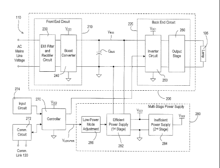
specifically, a multi-stage power supply for an electronic dimming ballast or
light-emitting diode
driver, where the power supply is able to operate in a low-power mode in which
the power
supply has a decreased power consumption.
BACKGROUND
[0003] Typical load control devices are operable to control the amount of
power
delivered to an electrical load, such as a lighting load or a motor load, from
an alternating-current
(AC) power source. One example of a typical load control device is a standard
dimmer switch,
which comprises a bidirectional semiconductor switch, such as a triac, coupled
in series between
the power source and the load. The semiconductor switch is controlled to be
conductive and
non-conductive for portions of a half-cycle of the AC power source to thus
control the amount of
power delivered to the load. A "smart" dimmer switch comprises a
microprocessor (or similar
controller) for controlling the semiconductor switch and a power supply for
powering the
microprocessor. In addition, the dimmer switch may comprise, for example, a
memory, a
- 1 -
CA 02754022 2011-08-31
WO 2010/101900 PCT/US2010/025894
communication circuit, and a plurality of light-emitting diodes (LEDs) that
are all powered by
the power supply.
[0004] Another example of a typical load control device is an electronic
dimming ballast,
which is operable to control the intensity of a gas discharge lamp, such as a
fluorescent lamp.
Electronic dimming ballasts typically comprise an inverter circuit having one
or more
semiconductor switches, such as field-effect transistors (FETs) that are
controllably rendered
conductive to control the intensity of the lamp. The semiconductor switches of
the inverter
circuit are often controlled by integrated circuit or a microprocessor. Thus,
a typical electronic
dimming ballast also comprises a power supply for powering the integrated
circuit or
microprocessor.
[0005] By decreasing the amount of power delivered to an electrical load,
a load control
device is operable to reduce the amount of power consumed by the load and thus
save energy.
However, the internal circuitry of the load control device (e.g., the
microprocessor and other
low-voltage circuitry) also consumes power, and may even consume energy when
the electrical
load is off (i.e., the load control device operates as a "vampire" load).
Thus, it is desirable to
reduce the amount of power consumed by a load control device, and
particularly, the amount of
standby power consumed by the load control device when the electrical load is
not powered.
SUMMARY
[0006] According to an embodiment of the present invention, a load
control device for
controlling the amount of power delivered from a power source to an electrical
load comprises a
load control circuit, a controller, and a multi-stage power supply that can
operate in a low-power
mode in which the power supply has a decreased power consumption. The load
control circuit is
adapted to be coupled between the source and the load for controlling the
power delivered to the
load. The controller is operatively coupled to the load control circuit and is
operable to control
the load control circuit to turn the electrical load off. The multi-stage
power supply comprises a
first efficient power supply operable to generate a first DC supply voltage
having a normal
magnitude in a non-nal mode of operation, and a second inefficient power
supply operable to
receive the first DC supply voltage and to generate a second DC supply voltage
for powering the
controller. The controller is coupled to the multi-stage power supply for
controlling the multi-
stage power supply to the low-power mode when the electrical load is off, such
that the
- 2 -
CA 02754022 2011-08-31
WO 2010/101900 PCT/US2010/025894
magnitude of the first DC supply voltage decreases to a decreased magnitude
that is less than the
normal magnitude and greater than the magnitude of the second DC supply
voltage. The
inefficient power supply continues to generate the second DC supply voltage in
the low-power
mode when the electrical load is off and the magnitude of the first DC supply
voltage has
decreased to the decreased magnitude.
[0007] According to another embodiment of the present invention, a multi-
stage power
supply for a load control device for controlling the amount of power delivered
to an electrical
load comprises: (1) a first efficient power supply operable to generate a
first DC supply voltage
having a normal magnitude in a normal mode of operation; (2) a second
inefficient power supply
operable to receive the first DC supply voltage and to generate a second DC
supply voltage for
powering the controller; and (3) a low-power mode adjustment circuit coupled
to the efficient
power supply for controlling the efficient power supply when the electrical
load is off, such that
the magnitude of the first DC supply voltage decreases to a decreased
magnitude that is less than
the nointal magnitude and greater than the magnitude of the second DC supply
voltage in the
low-power mode, and the inefficient power supply continues to generate the
second DC supply
voltage in the low-power mode.
[0008] Other features and advantages of the present invention will become
apparent from
the following description of the invention that refers to the accompanying
drawings.
BRIEF DESCRIPTION OF THE DRAWINGS
[0009] The invention will now be described in greater detail in the
following detailed
description with reference to the drawings in which:
[0010] Fig. 1 is a simplified block diagram of a load control system
having a plurality of
ballasts for control of the intensity of a plurality of fluorescent lamps
according to a first
embodiment of the present invention;
[0011] Fig. 2 is a simplified block diagram of one of the digital
electronic dimming
ballasts of the load control system of Fig. 1 according to the first
embodiment of the present
invention;
[0012] Fig. 3 is a two-stage power supply of the digital electronic
dimming ballast of Fig.
2;
- 3 -
CA 02754022 2011-08-31
WO 2010/101900 PCT/US2010/025894
[0013] Fig. 4 is a simplified flowchart of a control procedure executed
by a controller of
the digital electronic dimming ballast of Fig. 2;
[0014] Fig. 5 is a simplified block diagram of a light-emitting diode
(LED) driver for
controlling the intensity of a LED light source according to a second
embodiment of the present
invention; and
[0015] Fig. 6 is a simplified block diagram of a dimmer switch for
controlling the
amount of power delivered to a lighting load according to a third embodiment
of the present
invention.
DETAILED DESCRIPTION OF ILLUSTRATIVE EMBODIMENTS
[0016] The foregoing summary, as well as the following detailed
description of the
preferred embodiments, is better understood when read in conjunction with the
appended
drawings. For the purposes of illustrating the invention, there is shown in
the drawings an
embodiment that is presently prefened, in which like numerals represent
similar parts throughout
the several views of the drawings, it being understood, however, that the
invention is not limited
to the specific methods and instrumentalities disclosed.
[0017] Fig. 1 is a simplified block diagram of a fluorescent lighting
control system 100
for control of the intensity of a plurality of fluorescent lamps 105 according
to a first
embodiment of the present invention. The fluorescent lighting control system
100 includes two
digital electronic dimming ballasts 110 coupled to a digital ballast
communication link 120. The
ballasts 110 are each coupled to an alternating-current (AC) mains line
voltage and control the
amount of power delivered to the lamp 105 to thus control the intensities of
the lamps. The
control system 100 further comprises a link power supply 130 coupled to the
digital ballast
communication link 120. The link power supply 130 receives the AC mains line
voltage and
generates a DC link voltage for the digital ballast communication link 120.
The ballasts 110 are
operable to communicate with each other by transmitting and receiving digital
messages via the
communication link using, for example, the digital addressable lighting
interface (DALI)
protocol. The digital ballast communication link 120 may be coupled to more
ballasts 110, for
example, up to 64 ballasts. Each ballast 110 may further receive a plurality
of inputs from, for
- 4 -
CA 02754022 2011-08-31
WO 2010/101900 PCT/US2010/025894
example, an occupancy sensor 140, an infrared (IR) receiver 142, and a keypad
144, and to
subsequently control the intensities of the lamps 105 in response.
[0018] Fig. 2 is a simplified block diagram of one of the digital
electronic dimming
ballasts 110 according to the first embodiment of the present invention. The
electronic ballast
110 includes a load control circuit 200 coupled between the AC mains line
voltage and the lamp
105 for control of the intensity of the lamp. The load control circuit 200
comprises a front
end circuit 210 and a back end circuit 220. The front end circuit 210 includes
an EMI
(electromagnetic interference) filter and rectifier circuit 230 for minimizing
the noise provided
on the AC mains and for generating a rectified voltage from the AC mains line
voltage. The
front end circuit 210 further comprises a boost converter 240 for generating a
direct-current (DC)
bus voltage VBus across a bus capacitor CBus. The DC bus voltage VBus
typically has a
magnitude (e.g., 465 V) that is greater than the peak voltage VpK of the AC
mains line voltage
(e.g., 170 V). The boost converter 240 also operates as a power-factor
correction (PFC) circuit
for improving the power factor of the ballast 110. For example, the front end
circuit 210 may
comprise a semiconductor switch (not shown), a transformer (not shown), and a
PFC integrated
circuit (not shown), such as, part number TDA4863 manufactured by Infineon
Technologies AG.
The PFC integrated circuit renders the semiconductor switch to conductive and
non-conductive
to selectively conduct current through the transformer to thus generate the
bus voltage VBUS.
[0019] The back end circuit 220 includes an inverter circuit 250 for
converting the DC
bus voltage VBus to a high-frequency AC voltage. The inverter circuit 250
comprises one or
more semiconductor switches, for example, two FETs (not shown), and a ballast
control
integrated circuit (not shown) for controlling the FETs. The ballast control
integrated circuit is
operable to selectively render the FETs conductive to control the intensity of
the lamp 105. The
ballast control integrated circuit may comprise, for example, part number
NCP5111
manufactured by On Semiconductor. The back end circuit 220 further comprises
an output
circuit 260 comprising a resonant tank circuit for coupling the high-frequency
AC voltage
generated by the inverter circuit 250 to the filaments of the lamp 105.
[0020] A controller 270 is coupled to the inverter circuit 250 for
control of the switching
of the FETs to thus turn the lamp 105 on and off and to control (i.e., dim)
the intensity of the
lamp 105 between a minimum intensity (e.g., 1%) and a maximum intensity (e.g.,
100%). The
controller 270 may comprise, for example, a microcontroller, a programmable
logic device
(PLD), a microprocessor, an application specific integrated circuit (ASIC), or
any suitable type
- 5 -
CA 02754022 2013-05-16
of controller or control circuit. A communication circuit 272 is coupled to
the controller 270 and
allows the ballast 110 to communication (i.e., transmit and receive digital
messages) with the
other ballasts on the digital ballast communication link 120. The ballast 110
may further
comprise an input circuit 274 coupled to the controller 270, such that the
controller may be
responsive to the inputs received from the occupancy sensor 140, the IR.
receiver 142, and the
keypad 144. Examples of ballasts are described in greater detail in commonly-
assigned U.S.
Patent 7,489,090 entitled ELECTRONIC BALLAST HAVING
ADAPTIVE FREQUENCY SHIFTING; U.S. Patent No. 7,528,554
entitled ELECTRONIC BALLAST HAVING A BOOST CONVERTER WITH AN
IMPROVED RANGE OF OUTPUT POWER; and U.S. Patent Application No. 7,764,479
entitled COMMUNICATION CIRCUIT FOR A DIGITAL ELECTRONIC
DIMMING BALLAST.
[0021] The ballast 110 further comprises a multi-stage power supply 280
having a
low-power mode when the lamp 105 is off. The power supply 280 comprises two
stages: a first
efficient power supply (e.g., a switching power supply 282) and a second
inefficient power
supply (e.g., a linear power supply 284). The switching power supply 282
receives the DC bus
voltage Vgus and generates a first DC supply voltage Vi (e.g., having a normal
magnitude
VNORM of approximately 15 V). Alternatively, the switching power supply 282
could receive the
rectified voltage generated by the EMI filter and rectifier circuit 230 of the
front end circuit 210.
The PFC integrated circuit of the boost converter 240 and the ballast control
integrated circuit of
the inverter circuit 250 are powered by the first DC supply voltage Vcci. The
linear power
supply 284 receives the first DC supply voltage Vi and generates a second DC
supply voltage
Vcc2 (e.g., approximately 5 V) for powering the controller 270. Both the first
and second supply
voltages \Tech VCc2 are referenced to a circuit common of the ballast 110.
Alternatively, the
switching power supply 282 could be coupled directed to the AC mains line
voltage or to the
output of the EMI filter and rectifier circuit 230.
[0022] When the lamp 105 is on (i.e., the intensity of the lamp range from
the minimum
intensity of 1% to the maximum intensity 100%), the power supply 280 operates
in a normal
mode of operation. Specifically, the switching power supply 282 converts the
DC bus voltage
VBus (i.e., approximately 465 volts) to the first DC supply voltage Vcci
(i.e., the normal
magnitude VNORM of approximately 15 volts), such that there is a voltage drop
of approximately
450 volts across the switching power supply 282. Further, the linear power
supply 284 reduces
- 6 -
CA 02754022 2011-08-31
WO 2010/101900 PCT/US2010/025894
the first DC supply voltage Vcci to the second DC supply voltage Vcc2, such
that there is a
voltage drop of approximately 10 volts across the linear power supply.
Accordingly, there may
be a power loss of, for example, approximately 20 mW in the switching power
supply 282 and
approximately 360 mW in the linear power supply 284, such that the total power
loss of the two-
stage power supply is approximately 380 mW in the normal mode of operation.
[0023] The power supply 280 further comprises a low-power mode adjustment
circuit
286, which receives a low-power mode control signal VLOW-PWR from the
controller 270. The
low-power mode adjustment circuit 286 is coupled to the switching power supply
282, such that
the controller 270 is operable to control the operation of the power supply
280. When the lamp
105 is off (i.e., at 0%), the controller 270 drives the low-power mode control
signal VLOW-PWR
high (e.g., to approximately the second DC supply voltage Vcc2), such that the
power supply 280
operates in a low-power mode. At this time, the magnitude of the first DC
supply voltage Vcc1
generated by the switching power supply 282 decreases to a decreased magnitude
VDEC, which is
less than the normal magnitude VNORM and greater than the magnitude of the
second DC supply
voltage Vcc2. For example, the decreased magnitude VDEc may be approximately 8
volts. The
linear power supply 284 continues to generate the second DC supply voltage
Vcc2 when the
power supply 280 is operating in the low-power mode. Therefore, the controller
270 is still
powered and is operable to receive inputs from the input circuit 274 and to
transmit and receive
digital messages via the communication circuit 272 when the lamp 105 is off
and the power
supply 280 is operating in the low-power mode.
[0024] In the low-power mode, the voltage drop across the linear power
supply 284
decreases to approximately 3 volts. The average power loss of the linear power
supply 284 is
equal to approximately the voltage drop across the linear power supply
multiplied by the average
current drawn by the controller 270 and other low-voltage circuitry powered by
the second DC
supply voltage Vcc2. Thus, when the voltage drop across the linear power
supply 284 decreases
in the low-power mode, the power loss of the linear power supply also
decreases.
[0025] The decreased magnitude VDEc is less than the rated supply
voltages of the PFC
integrated circuit of the boost converter 240 and the ballast control
integrated circuit of the
inverter circuit 250. Therefore, when the magnitude of the first DC supply
voltage Vcc1
decreases from the non-nal magnitude VNoRm to the decreased magnitude VDEc in
the low-power
mode, the PFC integrated circuit of the boost converter 240 and the ballast
control integrated
circuit of the inverter circuit 250 stop operating. For example, the ballast
control integrated
- 7 -
CA 02754022 2011-08-31
WO 2010/101900 PCT/US2010/025894
circuit may comprise an under-voltage lockout (UVLO) feature that ensures that
the ballast
control integrated circuit does not render the controlled semiconductor
switches conductive when
the first DC supply voltage Vcci decreases to the decreased magnitude VDEc in
the low-power
mode. Since the boost converter 240 and the inverter circuit 250 do not
operate in the low-power
mode, there is minimal power dissipation in the transformer and the
semiconductor switches of
the boost converter and the inverter circuit, and the current drawn from the
first DC supply
voltage Vcci decreases, such that the ballast 110 consumes less power. In
addition, the
magnitude of the bus voltage Vmjs decreases to approximately the peak voltage
VpK of the AC
mains line voltage (i.e., approximately 170 V) because the boost converter 240
does not operate
in the low-power mode. Thus, the voltage drop across the switching power
supply 282 decreases
to approximately 162V volts in the low-power mode. As a result, there may be a
power loss of,
for example, approximately 7 mW in the switching power supply 282 and
approximately 120
mW in the linear power supply 284 in the low-power mode, such that the total
power loss in the
two-stage power supply 280 is approximately 127 mW. Accordingly, the two-stage
power
supply 280 operates more efficiently in the low-power mode than in the normal
mode.
[0026] Fig. 3 is a simplified schematic diagram of the two-stage power
supply 280. As
previously mentioned, the switching power supply 282 receives the bus voltage
VBus that is
generated by the boost converter 240. The switching power supply 282 comprises
a control
integrated circuit (IC) Ul, which includes a semiconductor switch, such as a
field-effect
transistor (FET), coupled between a drain terminal D and a source terminal S.
The control IC Ul
may comprise, for example, part number LNK304 manufactured by Power
Integrations. The
first DC supply voltage Vcci is generated across an energy storage capacitor
Cl (e.g., having a
capacitance of approximately 22 pf). An inductor Li is coupled between the
capacitor Cl and
the source teiminal of the control IC Ul and has, for example, an inductance
of approximately
1500 pH. A diode D1 is coupled between the circuit common and the source
terminal of the
control IC Ul. As shown in Fig. 3, the FET of the control IC Ul, the inductor
Li, the capacitor
Cl, and the diode D1 form a standard buck converter. Alternatively, a
different switching power
supply topology could be used to generate the first DC supply voltage Vcci
from the bus voltage
VBUS=
[0027] The switching power supply 282 further comprises a feedback
circuit comprising
two diodes D2, D3, a zener diode Z1, a capacitor C2, and two resistors R1, R2.
The feedback
circuit is coupled between the DC supply voltage Vcci and a feedback terminal
FB of the control
- 8 -
CA 02754022 2011-08-31
WO 2010/101900 PCT/US2010/025894
IC UI . The control IC Ul renders the FET conductive and non-conductive to
selectively charge
the capacitor Cl, such that a feedback voltage at the feedback teiminal FB is
maintained at a
specific magnitude, e.g., approximately 1.65 volts. For example, the zener
diode Z1 has a break-
over voltage VB0 of approximately 6.2V, the resistor R1 has a resistance of
approximately 5.11
kc1, and the resistor R2 has a resistance approximately 2.00 kO, such that the
DC supply voltage
Vcci generated by the switching power supply 282 has the normal magnitude
VN0Rm of
approximately 15 volts in the noimal mode of operation. The capacitor C2 has,
for example, a
capacitance of approximately 1.0 F.
[0028] The switching power supply 282 also comprises a bypass capacitor
C3 for use by
an internal power supply of the control IC Ul. The bypass capacitor C3 is
coupled between a
bypass terminal BP and the source terminal S of the control IC Ul, and has,
for example, a
capacitance of approximately 0.1 F. The bypass capacitor C3 is operable to
charge from the
control IC Ul through the bypass terminal BP. However, to allow for more
efficient operation,
the bypass capacitor C3 is also operable to charge from the DC bus voltage
Vcc1 through the
zener diode Z1, the diode D3, a resistor R3 (e.g., having a resistance of
approximately 2.321d2),
and another diode D4.
[0029] The linear power supply 284 receives the first DC supply voltage
Vcc1 and
generates the second DC supply voltage Vcc2. The linear power supply 284
comprises a linear
regulator U2, which operates to produce the second DC supply voltage Vcc2
across a capacitor
C4 (e.g., having a capacitance of approximately 10 p.F). The linear regulator
U2 may comprise,
for example, part number MC78L05A manufactured by On Semiconductor. The
decreased
magnitude VDEc (i.e., approximately 8 V) is greater than a rated dropout
voltage of the linear
regulator U2 (e.g., approximately 6.7 V) below which the linear regulator U2
will stop
generating the second DC supply voltage Vcc2. Therefore, the linear power
supply 284
continues to generate the second DC supply voltage Vcc2 when the power supply
280 is
operating in the low-power mode.
[0030] The low-power mode adjustment circuit 286 is coupled to the
switching power
supply 282 and receives the low-power mode control signal VLow_pwR from the
controller 270.
The controller 270 drives the low-power mode control signal VLOW-PWR low
(i.e., to
approximately circuit common) to operate the power supply 280 in the nolinal
mode when the
lamp 105 is on and drives the low-power mode control signal VLow-pwR high
(i.e., to
approximately the second DC supply voltage Vcc2) to operate the power supply
in the low-power
- 9 -
CA 02754022 2011-08-31
WO 2010/101900 PCT/US2010/025894
mode when the lamp is off. The low-power mode adjustment circuit 286 comprises
a PNP
bipolar junction transistor (BJT) Q1 coupled across the zener diode Z1 of the
switching power
supply 282. A resistor R4 is coupled between the emitter and the base of the
transistor Q1 and
has a resistance of, for example, approximately 10 ka The low-power mode
control signal
VLow_pwR is coupled to the base of an NPN bipolar junction transistor Q2
through a resistor R5
(e.g., having a resistance of approximately 4.991d2). A resistor R6 is coupled
between the base
and the emitter of the transistor Q2 and has a resistance of approximately 10
kf2.
[0031] When the low-power mode control signal VLOW-PWR is low, both of
the transistors
Q1 , Q2 are non-conductive, and thus, the switching power supply 282 operates
to generate the
first DC supply voltage Vcci at the flotilla' magnitude VNoRm of approximately
15 V as
described above. However, when the low-power mode control signal VLOW-PWR is
driven high by
the controller 270, the transistor Q2 is rendered conductive and the base of
the transistor Q1 is
pulled down towards circuit common through a resistor R7 (e.g., having a
resistance of
approximately 6.81 IS1). Accordingly, the transistor Q1 is rendered
conductive, thus, "shorting
out" the zener diode Z1 of the switching power supply 282. Since the zener
diode Z1 is
essentially removed from the feedback circuit of the switching power supply
282, the control IC
Ul now operates to maintain the magnitude of the first DC supply voltage Vcci
at the decreased
magnitude VD.Ec. In other words, the magnitude of the first DC supply voltage
Vcci is no longer
dependent upon the breakover voltage Vpo of the zener diode Zl. The decreased
magnitude VDEc is approximately equal to the difference between the nomial
magnitude VNORM
of the first DC supply voltage Vcci and the breakover voltage VB0 of the zener
diode Zl.
[0032] Fig. 4 is a simplified flowchart of a control procedure 300
executed by the
controller 270 of the ballast 110 in response to receiving a command to change
the intensity of
the lamp 105 at step 310, e.g., in response to digital messages received via
the communication
circuit 272 or in response to inputs received from the occupancy sensor 140,
the IR receiver 142,
and the keypad 144 via the input circuit 274. If the received command is to
turn the lamp 105
off at step 312, the controller 270 controls the inverter circuit 250 to
control the intensity of the
lamp to 0% at step 314 and drives the low-power mode control signal VLOW-PWR
high to operate
the power supply 280 in the low-power mode at step 316, before the control
procedure 300 exits.
If the received command is not to turn the lamp 105 off at step 312, the
controller 270 adjusts
intensity of the lamp according to the received command (e.g., to a specific
intensity) at step 318
- 10 -
CA 02754022 2013-05-16
=
and drives the low-power mode control signal Vinw-pwR low to operate the power
supply 280 in
the normal mode at step 320, before the control procedure 300 exits.
[0033] Fig. 5 is a simplified block diagram of an LED driver 400 for
controlling the
intensity of an LED light source 405 according to a second embodiment of the
present invention.
The LED driver 400 comprises a front end circuit 410 including an EMI filter
and rectifier circuit
430 and a buck converter 440 for generating a direct-current (DC) bus voltage
VBus that has a
magnitude less than the peak voltage VpK of the AC mains line voltage (e.g.,
approximately 60
V). Alternatively, the buck converter 440 could be replaced by a boost
converter, a buck/boost
= converter, or a flyback converter. The LED driver 400 also includes a
back end circuit 420,
which comprises an LED load control circuit 450, and a controller 470 for
controlling the
operation of the LED load control circuit 450. As in the first embodiment, the
multi-stage power
supply 280 comprises the switching power supply 282, the linear power supply
284, and the low-
power mode adjustment circuit 286. The controller 470 is operable to control
the multi-stage
power supply 280 to the low-power mode when the LED light source 405 is off
(as in the first
embodiment of the present invention).
[0034] The LED load control circuit 450 receives the bus voltage
VBus and regulates the
magnitude of an LED output current 'LED conducted through the LED light source
405 (by
controlling the frequency and the duty cycle of the LED output current 'LED)
in response to the
controller 470 to thus control the intensity of the LED light source. For
example, the LED load
control circuit 450 may comprise a LED driver integrated circuit (not shown),
for example, part
number MAX16831, manufactured by Maxim Integrated Products. To control the
intensity of
the LED light source 405, the LED load control circuit 450 may be operable to
adjust the
magnitude of the LED output current 'LED or to pulse-width modulate (PWM) the
LED output
current.
[0035] Fig. 6 is a simplified block diagram of a dimmer switch 500
for controlling the
amount of power delivered from an AC power source 502 to a lighting load 505,
such as an
incandescent lamp, according to a third embodiment of the present invention.
The dimmer
switch 500 comprises a load control circuit 530 (e.g., a dimmer circuit)
coupled in series
electrical connection between the AC power source 502 and the lighting load
505, and a
- 11 -
CA 02754022 2013-05-16
controller 570 for controlling the operation of the load control circuit and
thus the intensity of the
lighting load.
[0036] The dimmer switch 500 may be adapted to be mounted to a standard
electrical
wallbox (i.e., replacing a standard light switch), and may comprise one or
more actuators 572 for
receiving user inputs. The controller 570 is operable to toggle (i.e., turn on
and off) the lighting
load 505 and to adjust the amount of power being delivered to the lighting
load in response to the
inputs received from the actuators 572.
[0037] The controller 570 may be further coupled to a communication circuit
574 for
transmitting and receiving digital messages via a communication link, such as
a wired
communication link or a wireless communication link, e.g., a radio-frequency
(RF)
communication link or an infrared (IR) communication link. The controller 570
may be operable
to control the controllably conductive device 574 in response to the digital
messages received via
the communication circuit 574. Examples of RF load control systems are
described in greater
detail in U.S. Patent 7,573,208 entitled METHOD OF
PROGRAMMING A LIGHTING PRESET FROM A RADIO-FREOUENCY REMOTE
CONTROL, and U.S. Patent Application 2009-0206983 entitled
COMMUNICATION PROTOCOL FOR A RADIO-FREQUENCY LOAD CONTROL
SYSTEM. An example of an IR load control system is described in greater detail
in U.S. Patent
No. 6,545,434, issued April 8, 2003, entitled MULTI-SCENE PRESET LIGHTING
CONTROLLER.
[0038] The load control circuit 530 includes a controllably conductive
device (e.g., a
bidirectional semiconductor switch 550) adapted to conduct a load current
through the lighting
load 505, and a drive circuit 552 coupled to a control input (e.g., a gate) of
the bidirectional
semiconductor switch for rendering the bidirectional semiconductor switch
conductive and
non-conductive in response to control signals generated by the controller 570.
The bidirectional
semiconductor switch 550 may comprise any suitable type of controllable
switching device, such
as, for example, a triac, a field-effect transistor (FET) in a rectifier
bridge, two FETs in anti-
series connection, or two or more insulated-gate bipolar junction transistors
(IGBTs). A zero-
crossing detector 576 is coupled across the bidirectional semiconductor switch
550 and
determines the zero-crossings of the AC mains line voltage of the AC power
supply 502, i.e., the
times at which the AC mains line voltage transitions from positive to negative
polarity, or from
- 12-
CA 02754022 2013-05-16
negative to positive polarity, at the beginning of each half-cycle. Using a
standard phase-control
technique, the controller 576 selectively renders the bidirectional
semiconductor switch 550
conductive at predetermined times relative to the zero-crossing points of the
AC mains line
voltage, such that the bidirectional semiconductor switch is conductive for a
portion of each half-
cycle of the AC mains line voltage. Typical dimmer circuits are described in
greater detail in
U.S. Patent No. Patent No. 5,248,919, issued September 29, 1993, entitled
LIGHTING
CONTROL DEVICE, and U.S. Patent No. 7,242,150, issued July 10, 2007, entitled
DIMMER
HAVING A POWER SUPPLY MONITORING CIRCUIT.
[00391 The dimmer switch 500 comprises a multi-stage power supply 580 that
operates
in a low-power mode when the lighting load 505 is off (as in the first and
second embodiments
of the present invention). The power supply 580 comprises a first efficient
power supply (e.g., a
switching power supply 582) and a second inefficient power supply (e.g., a
linear power
supply 584). The power supply 580 also comprises a rectifier bridge 588 and a
capacitor CR for
generating a rectified voltage, which is provided to the switching power
supply 582. As in the
first and second embodiments, a low-power mode adjustment circuit 586 controls
the power
supply into the low-power mode in response to a low-power mode control signal
VLOW-PWR
received from the controller 570. Specifically, the controller 570 controls
the power supply 580
to the low-power mode when the lighting load 505 is off.
[0040] While the present invention has been described with reference to the
ballast 110,
the LED driver 400, and the dimmer switch 500, the multi-stage power supply
280, 480 of the
present invention could be used in any type of control device of a load
control system, such as,
for example, a remote control, a keypad device, a visual display device, an
electronic switch, a
switching circuit including a relay, a controllable plug-in module adapted to
be plugged into an
electrical receptacle, a controllable screw-in module adapted to be screwed
into the electrical
socket (e.g., an Edison socket) of a lamp, a motor speed control device, a
motorized window
treatment, a temperature control device, an audio/visual control device, or a
dimmer circuit for
other types of lighting loads, such as, magnetic low-voltage lighting loads,
electronic low-
voltage lighting loads, and screw-in compact fluorescent lamps.
[00411 Although the present invention has been described in relation to
particular
embodiments thereof, many other variations and modifications and other uses
will become
apparent to those skilled in the art. It is preferred, therefore, that the
present invention be limited
- 13 -
CA 02754022 2011-08-31
WO 2010/101900
PCT/US2010/025894
not by the specific disclosure herein, but only by the appended claims.
- 14 -