Note: Descriptions are shown in the official language in which they were submitted.
CA 02754062 2011-08-31
WO 2010/099597 PCT/CA2010/000260
-1-
NAND FLASH ARCHITECTURE WITH MULTI-LEVEL ROW DECODING
CROSS REFERENCE TO RELATED APPLICATION
[0001] This application claims the benefit of US Provisional Application
No. 61/157,594, filed March 5, 2009 and U.S. Application No. 12/495,089 filed
June 30, 2009, the contents which are incorporated herein by reference in
their
entirety.
FIELD
[0002] A NAND flash memory device is disclosed.
BACKGROUND
[0003] In conventional NAND flash memory, erasing is performed on a per-
block basis. In contrast, read and program operation takes place on a per-page
basis.
BRIEF DESCRIPTION OF THE DRAWINGS
[0004] Example embodiments will now be described with reference to the
attached drawings in which:
FIG. 1 is a block diagram of a typical memory core architecture in NAND
flash memory;
FIG. 2 is a block diagram of an example NAND flash device within which
one of the NAND core architectures described herein might be implemented;
FIG. 3 is a block diagram of memory core architecture for NAND flash
memory provided by an example embodiment;
FIG. 4 is a block diagram of a memory core architecture in a NAND flash
memory provided by an example embodiment;
FIGS. 5 and 6 show single page read and multiple page read operation
for the example embodiment of Figure 3, respectively;
CA 02754062 2011-08-31
WO 2010/099597 PCT/CA2010/000260
-2-
FIG. 7 is a block diagram of a memory core architecture in NAND flash
memory in accordance with an example embodiment;
FIG. 8 is a block diagram of a global row decoder in accordance with an
example embodiment;
FIG. 9 is a circuit diagram of an example implementation of a single
block decoder of Figure 8;
FIG. 10 is a block diagram of another example implementation of a
single block decoder of Figure 8;
FIG. 11 is a block diagram of a local row decoder in accordance with an
example embodiment;
FIG. 12 is a circuit diagram of an example implementation of a single
sector decoder of Figure 10;
FIG. 13 is a timing diagram for read in accordance with an example
embodiment;
FIG. 14 is a timing diagram for program in accordance with an example
embodiment; and
FIG. 15 is a timing diagram for erase in accordance with an example
embodiment.
DETAILED DESCRIPTION
[0005] FIG. 1 illustrates a memory core architecture in a NAND flash memory.
The NAND flash memory core comprises a NAND memory cell array 100, a row
decoder 102 and a page buffer circuit 103 and column decoder 104. The row
decoder
102 is connected to the NAND memory cell array 100 by a set of wordlines, only
one
wordline 106 being shown in FIG. 1 for simplicity. The page buffer circuit 103
is
connected to the NAND memory cell array 100 through a set of bitlines, only
one
bitline 108 being shown in FIG. 1 for simplicity.
CA 02754062 2011-08-31
WO 2010/099597 PCT/CA2010/000260
-3-
[0006] The cell array structure of the NAND flash memory comprises a set of n
erasable blocks. Each block is subdivided into m programmable pages (rows).
[0007] Erasing for the memory core architecture of FIG. 1 is performed on a
per- block basis. In contrast, read and program operation takes place on a per-
page
basis.
[0008] A NAND flash memory having the core architecture of FIG. 1 flash
suffers from at least three limitations. First, bits can only be programmed
only after
erasing a target memory array. Second, each cell can only sustain a limited
number of
erasures, after which it can no longer reliably store data. In other words,
there is a
limitation in the number of erase and program cycle to cells (i.e. endurance,
typically
10,000 - 100,000 cycles). Third, the minimum erasable array size is much
bigger than
the minimum programmable array size. Due to these limitations, sophisticated
data
structures and algorithms are implemented to effectively use flash memories.
[0009] When the flash controller requests data write or data modification into
even only a small portion of the page, typically the block containing a page
to be
modified will be reprogrammed to one of free (empty) blocks declared by an
erase-unit
reclamation process. In this case, valid pages containing original data in the
original
block are copied to the selected free block. After that, the new block having
modified
data in a page with original data in the rest of pages is remapped to the
valid block
address by a virtual mapping system in the flash controller. The original
block is now
obsolete and will be declared as a free block by the erase-unit reclamation
process
after it has been erased.
[0010] The limited number of erase-program cycles (endurance) limits the
lifetime of a flash device. It would be advantageous to have a lifetime that
is as long as
possible, and this depends on the pattern of access to the flash device.
Repeated and
frequent rewrites to a single cell or to a small number of cells will bring
the onset of
failures soon and so end the useful lifetime of the device quickly.
CA 02754062 2011-08-31
WO 2010/099597 PCT/CA2010/000260
-4-
[0011] Moreover, in a flash memory system having multiple flash devices, if
there is significantly uneven use among devices in the flash memory system,
one
device will reach an end of lifetime at a time when other devices have
significant life
left in them. When the one device reaches an end of life time, the entire
memory
system may have to be replaced, and this greatly reduces the life time of the
flash
memory system.
[0012] If rewrites can be evenly distributed to all cells of the device, the
onset of
failures will be delayed as much as possible, maximizing the lifetime of the
device. To
extend the device lifetime by even use across all the cells of the device,
many wear-
levelling techniques and algorithms have been proposed and implemented in
flash
memory systems.
[0013] The cell arrays of NAND flash have been so miniaturized over the
course of time that they have reached the point where any further reduction in
process
technology is expected to drastically reduce the maximum number of erase-
program
cycles.
[0014] According to one broad aspect, provided is a NAND flash memory core
with multi-level row decoding.
[0015] According to another broad aspect, provided is a NAND flash memory
device comprising: peripheral circuitry, input/output pads, and a high voltage
generator; a NAND flash memory core comprising: a NAND memory cell array
comprising a plurality of rows by a plurality of columns, the cells arranged
into a
plurality of sectors, each sector comprising the cells of a plurality of said
columns; the
cells arranged into a plurality of blocks, each block comprising cells of a
plurality of
said rows; the NAND memory cell array configured for erasure to a resolution
of one
block within one sector, and configured for read and program to a resolution
of one
row within one sector.
CA 02754062 2011-08-31
WO 2010/099597 PCT/CA2010/000260
-5-
[0016] According to another broad aspect of, provided is a method in a NAND
flash memory core comprising: performing multi-level row decoding. Due to the
size
mismatch between read/program and erase, the block copy operations described
above introduce unnecessary program operations because unaffected data in
pages
of the block are reprogrammed (copied) to the new block along with the
modified data.
There could be a dramatic extension to the device lifetime if the minimum
erasable
array size is smaller than an entire block.
[0017] FIG. 2 is a block diagram of a device 150 containing a NAND flash
memory device 152. The NAND flash memory device 152 has a memory core with
multi-level row decoding, generally indicated at 158. In addition, the NAND
flash
memory device 152 has a peripheral circuitry 154, input and output pads 156,
and
high voltage generator(s) 160. The peripheral circuitry 154 may, for example,
comprise one or more of input and output buffers for address and data, input
buffers
for control and command signals, state machine including command decoder,
address
counter, row and column per-decoder, and status registers. Device 150 may be
any
device having a use for NAND flash memory device 152. Specific examples
include a
mobile device, a memory stick, a camera, a solid state disk drive, and an MP3
player.
Flash device 152 may form a permanent part of the device 150, or may be
removable.
Detailed example implementations of the memory core with multi-level row
decoding
are provided below. More generally, any memory core with multi-level row
deciding is
contemplated. The cell array is formed of sectors, each sector comprising a
plurality
of columns of cells. The cells also form blocks, each block comprising a
plurality of
rows, also referred to as pages. In some embodiments, multi-level row decoding
involves performing a first level of row decoding for all of the sectors, and
for each
sector, performing a second level of row decoding only for that sector. In
some
embodiments, erasing within the memory core is performed to a resolution of
one
block within one sector, and read and program operations take place to a
resolution of
one row within one sector.
CA 02754062 2011-08-31
WO 2010/099597 PCT/CA2010/000260
-6-
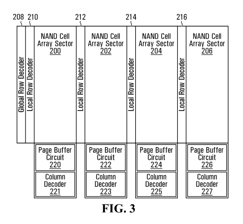
[0018] Referring now to FIG. 3, shown is a core architecture provided by an
example embodiment. The core architecture includes a NAND memory cell array
that
is implemented as at least two NAND memory cell array sectors, hereinafter
simply
"sectors", there being four sectors 200,202,204,206 shown in the illustrated
example.
The NAND memory cell array is formed of a plurality of blocks which in turn
are
formed of pages, also referred to as rows. The cells of each sector of the
NAND
memory cell array are also arranged in columns (not shown). Row decoding
functionality is provided by a global row decoder 208 that performs row
decoding to
the level of blocks, in combination with a set of local row decoders
210,212,214,216
that perform decoding to the level of a page within a block selected by the
global row
decoder. More generally, the global row decoder 208 performs a first level of
row
decoding to select a subset of the plurality of rows. In example embodiments
described herein in detail, the selectable subsets are contiguous blocks, but
this need
not be the case in all implementations. The local row decoders 210, 212, 214,
216
perform a second level of row decoding to select a row within the subset of
the
plurality of rows selected by the global row decoder 208. The local row
decoders
210,212,214,216 include one local row decoder associated with each respective
sector 200,202,204,206 and perform page selection local to the associated
sector.
Page buffer functionality is implemented with four page buffer circuits
220,222,224,226, one per sector 200,202,204,206. Column decoder functionality
is
implemented with four column decoders 221,223,225,227, one per sector
200,202,204,206.
[0019] Read operation is performed to the resolution of a page within a block
within a sector. Program operation is also performed to the resolution of a
page within
a block within a sector. However, a page within a block within a sector is
erased
before it is programmed. Erase operation is performed to the resolution of a
block
within a sector.
CA 02754062 2011-08-31
WO 2010/099597 PCT/CA2010/000260
-7-
[0020] For a read operation, the global row decoder 208 is used to select a
block of the plurality of blocks of the NAND memory cell array. Sector
selection is
performed by performing column selection with the page buffer circuit and
column
decoder associated with the desired memory sector. This can be achieved, for
example, by a memory controller enabling the associated page buffer circuit
and
column decoder and/or sending column decoder signals to the associated page
buffer
circuit and column decoder. Page selection is performed by the local row
decoder
associated with the selected sector. In this manner, a selected page within a
selected
block within a selected sector can be read. During a read operation, the data
of the
selected page within the selected block and within the selected sector is
sensed and
latched into sense amplifier (not shown) and page buffer circuit of the
selected sector.
After that the data stored in the page buffer circuit is sequentially read out
through the
associated column decoder and, for example, stored in a global buffer (not
shown).
[0021] For an erase operation, the global row decoder 208 is used to select a
block of the plurality of blocks of the NAND memory cell array. Sector
selection is
performed by performing column selection with the page buffer circuit and
column
decoder associated with the desired memory sector. Then an appropriate erase
signal is applied. In this manner, a selected block within a selected sector
can be
erased.
[0022] For a program operation, the global row decoder 208 is used to select a
block of the plurality of blocks of the NAND memory cell array. Sector
selection is
performed by performing column selection with the page buffer circuit and
column
decoder associated with the desired memory sector. Page selection is performed
by
the local row decoder associated with the selected sector. Then, the contents
of the
page buffer circuit associated with the selected sector are programmed to the
selected
page within the selected block within the selected sector. During a program
operation,
the input data (for example from a global buffer circuit, not shown) is
sequentially
loaded into the page buffer circuit of the selected sector via the associated
column
decoder. The input data latched in the page buffer circuit is then programmed
into the
selected page of the selected sector.
CA 02754062 2011-08-31
WO 2010/099597 PCT/CA2010/000260
-8-
[0023] FIG. 4 shows another example of a core architecture provided by an
example embodiment. This example embodiment is similar to FIG. 2 and like
components have been labelled using like reference numbers. The example
embodiment of FIG. 4 has a block pre-decoder 230 connected through block
decoder
lines 231 to the global row decoder 208. The global row decoder 208 is
connected to
the memory array through a plurality of blocklines, one per block although
only one
blockline 240 is shown in the illustrated example. The blocklines are commonly
connected to all local row decoders 210,212,214,216. Each local row decoder
210,212,214,216 is also driven by a respective set of page decoder lines
233,235,237,239 from a respective page decoder 232,234,236,238. Each local row
decoder 210,212,214,216 is connected to the corresponding sector though a
plurality
of wordlines, only one shown per sector indicated at 211,213,215,219.
[0024] In operation, to select a particular block, the block pre-decoder 230
converts an input, for example from a memory controller, into an appropriate
signal on
block decoder lines 231. The global row decoder 208 selects one of block
lines. To
select a particular page within a particular sector, the page decoder of the
associated
sector (one of page decoders 232,234,236,238) is enabled and used to select
the
particular page within the selected block.
[0025] An example of single sector selection is depicted in FIG. 5 which shows
selection of a page within a block for local row detector 210. In some example
embodiments, the circuit is configured to allow multiple page decoders to be
enabled
simultaneously. In such example embodiments, within the selected block,
selection of
a respective page within multiple sectors can be performed by enabling
multiple page
decoders. An example of multiple sector selection is shown in FIG. 6 which
shows
selection of a row within a block by each of row decoders 210 and 214. The
blockline
selects one of blocks within all of the sectors while page decoder lines
select one of
pages (i.e. wordlines) within the selected block in each sector.
CA 02754062 2011-08-31
WO 2010/099597 PCT/CA2010/000260
-9-
[0026] In this example embodiment, a read operation will result in one or
multiple page buffer circuits containing read-out data. The contents of these
page
buffer circuits are then individually read out. A program operation will
result in the
contents of one or multiple page buffer circuits being programmed
simultaneously.
Typically, this will have been preceded by a series of write to page buffer
operations
by which the multiple page buffer circuits are written to sequentially.
[0027] FIG. 7 shows more detailed core architecture provided by an example
embodiment wherein again this example embodiment is similar to FIG. 3 and like
components have been labelled using like reference numbers. In FIG. 7, as in
other
block diagrams, certain components (such as, for example, column decoders) are
not
shown so as not to obscure features of example embodiments. In the example, a
NAND core (this can be an entire device core architecture, a plane or a bank)
comprises four sectors and the page size of each sector is 512 bytes. More
generally,
the page size of each sector is at least one byte. In this example, there are
2048
blocks collectively indicated at 217. Each block is split into four sectors.
The global
row decoder 208 is connected to all of the local row decoders 210, 212, 214,
216 in
common by 2048 blocklines (not shown), one per block. Each block has 32 pages.
[0028] An example implementation of the global row decoder 208 of FIG. 7 is
depicted in FIG. 8. The global row decoder 208 has a respective block decoder
for
each block, namely 2048 block decoders collectively indicated at 209
corresponding to
the number of blocks. Each of the block decoders is connected to the block
decoder
lines 231. In this example, the block decoder lines 231 comprises lines
xp,xq,xr,xt for
carrying block decoder address signals Xp,Xq,Xr and Xt. Xp,Xq,Xr and Xt are
the pre-
decoded lines. Xp corresponds to Address A0-A2. Xq corresponds to Address A3-
A5.
Xr corresponds to Address A6-A8. Xt corresponds to Address A9-A10 Each block
decoder drives a respective blockline (not shown). The block decoder
associated with
the block indicated by the address signals on block decoder lines 231 drives
the
respective blockline to be in a select state, and all other blocklines are in
a de-select
state.
CA 02754062 2011-08-31
WO 2010/099597 PCT/CA2010/000260
-10-
[0029] An example circuit implementation of a single block decoder is depicted
in FIG. 9. It is noted that there are many variations on circuit
implementation for the
block decoder, and that such variations should be readily apparent to one
skilled in the
art.
[0030] The circuit has a block decoder address latch 302 having a latch output
BDLCH_out that is reset to OV when the RST_BD is high (actually short pulse)
and
latched when the LCHBD is high (which may be a short pulse) with valid
predecoded
address signals of Xp, Xq, Xr and Xt (block decoder lines) received at NAND
logic
gate 303. Detailed timing information is shown in FIGS. 12, 13 and 14
described
subsequently.
[0031] The block decoder has a local charge pump 300 that is a high voltage
switching circuit to provide voltages during read, program and erase
operations. Local
charge pump 300 includes a depletion mode n-channel pass transistor 352, a
native
n-channel diode-connected boost transistor 354, a high breakdown voltage n-
channel
decoupling transistor 356, a high breakdown voltage n-channel clamp transistor
358, a
NAND logic gate 360, and a capacitor 362. NAND logic gate 360 has one input
terminal for receiving the latch output BDLCH_out and another input terminal
for
receiving control signal OSC, for driving one terminal of capacitor 362. Pass
transistor
352 is controlled by the complement of signal HVen, referred to as HVenb. The
common terminals of decoupling transistor 356 and clamp transistor 358 are
coupled
to high voltage Vhv.
[0032] The final output signal BD_out of the each block decoder is commonly
connected to all of the local row decoders, for example as depicted in FIG. 9.
CA 02754062 2011-08-31
WO 2010/099597 PCT/CA2010/000260
-11-
[0033] The operation of local charge pump 350 will now be described. During a
read operation, HVenb is at the high logic level and OSC is maintained at the
low logic
level. Therefore, circuit elements 362, 354, 356 and 358 are inactive, and the
output
terminal BD_out reflects the logic level appearing on BDLCH_out. During a
program
operation, HVenb is at the low logic level, and OSC is allowed to oscillate
between the
high and low logic levels at a predetermined frequency. If the latch output
BDLCH_out
is at the high logic level, then capacitor 362 will repeatedly accumulate
charge on its
other terminal and discharge the accumulated charge through boost transistor
354.
Decoupling transistor 356 isolates Vhv from the boosted voltage on the gate of
boost
transistor 354. Clamp transistor 358 maintains the voltage level of output
terminal
BD_out at about Vhn+Vth, where Vth is the threshold voltage of clamp
transistor 358.
The local charge pump 300 shown in FIG. 9 is one example circuit which can be
used
to drive signals to a voltage levels higher than the a supply voltage VCC, but
persons
skilled in the art will understand other charge pump circuits can be used with
similar or
equal effectiveness. Table 1 below shows example bias conditions for the local
charge
pump 300 during read and program operations.
TABLE 1
Read Program
Selected Unselected Selected Unselected
BDLCH_out Vcc Vss Vcc Vss
Hvenb Vss Vss Vss Vss
OSC Oscillation Oscillation Oscillation Oscillation
Vhn Vread7 Vread7 (-7V) -Vpgm -Vpgm
(-7V) (14V-18V) (14V-18V)
BD_out Vread7 Vss Vpgm Vss
(-7V)+Vth (1 4V- 1 8V)+
Vth
CA 02754062 2011-08-31
WO 2010/099597 PCT/CA2010/000260
-12-
[0034] The output signal BD_out of the block decoder is raised to Vhv when the
block decoder latch output BDLCH_out is Vcc, HVenb is OV and the OSC is
oscillating.
[0035] Referring to FIG. 10, another example of a block decoder uses a block
selection transistor. Vhwl is a high voltage source which has various levels
based on
operations. In this example embodiment, the drivability of BD_out is
determined by the
size of the block selection transistor, not the local charge pump. Therefore
this circuit
provides stronger drivability in the case of higher number of local row
decoders in the
NAND memory core.
[0036] FIG. 11 depicts an example of a local row decoder. The local row
decoder has 2048 sector decoders collectively indicated at 500, one per block.
These are referred to as sector decoders because a page within a sector is
selected,
as opposed to a page within the overall memory array. The inputs to the local
row
decoder are page decoder lines which in the illustrated example include string
select
(SS), wordline select signals S0-S31 (one per wordline), and ground select
(GS). The
wordline select signals S0-S31 commonly connect to the sector decoders.
[0037] Referring now to FIG. 12, an example circuit for a single sector
decoder
will be described. String select line SSL, wordlines WLO to WL31 and ground
select
line GSL are driven by common signals of SS, SO to S31 and GS through pass
transistors TSS, TS0 to TS31 and TGS which are commonly controlled by the
output
signal BD_out of the associated block decoder. The page decoder lines, namely
string
select signal SS, ground select signal GS and common string decode signals SO
to
S31, are provided by the page decoder.
CA 02754062 2011-08-31
WO 2010/099597 PCT/CA2010/000260
-13-
[0038] In operation, for the block that is selected, the BD_out input of all
the
corresponding sector decoders is activated. This will include one sector
decoder for
that block in each sector. For all the remaining blocks that were not
selected, the
BD_out of all the corresponding sector decoders is deactivated. For a sector
for which
an operation is to be performed, within that sector, all of the sector
decoders are
commonly controlled by common page decoder lines. There may be one or more
sectors for which an operation is to be performed. For a sector for which no
operation
is to be performed, all of the common page decoder lines are inactive such
that all of
the commonly connected sector decoders are inactive. For a sector decoder that
is
selected both by a BD_out in a select state, and by page decoder lines that
are active,
the sector decoder causes a respective selected wordline (one of WL0 through
WL31)
to be in a selected state while the remaining wordlines are in a de-selected
state.
[0039] Table 2 shows an example set of bias conditions to the block decoder,
local row decoder and NAND cell array during read, program and erase. It is to
be
understood that all values may vary based on cell characteristics and process
technology.
TABLE 2
Read Program Erase
Selected Global Row Vread7 (-7V) + Vpgm+Vth Vcc
Decoder: BD out Vth
Unselected Global Vss (OV) Vss (OV) Vss (OV)
Row Decoder:
BD_out
Local Decoder in Selected Sector
SS Vread (4 - 5V) 2V - Vcc Floating and Vcc-
Vth (Self-booting)
CA 02754062 2011-08-31
WO 2010/099597 PCT/CA2010/000260
-14-
Selected Si Vss (0V) Vpgm (14V - 18V) Vss (OV)
Unselected Si Vread (4 - 5V) Vpass (8V - 12V) -
SSL Vread (4 - 5V) 2V - Vcc Floating & Self-
boosting (70 - 90%
of Vers)
Selected WLi Vss (0V) Vpgm (14V - 18V) Vss (OV)
Unselected WLi Vread (4 - 5V) Vpass (8V - 12V) -
GS Vread (4 - 5V) Vss (0V) Floating and Vcc-
Vth (Self-booting)
GSL Vread (4 - 5V) Vss (OV) Floating & Self-
boosting (70 - 90%
of Vers)
Bitlines Pre-charged & Vss (OV) for Clamp to Vers-0.6V
Sensed program & Vcc for
Program Inhibit
Cell Substrate Vss (OV) Vss (OV) Vers (- 20V)
Local Decoder in Unselected Sector
SS Vss (OV) Vss (OV) Vss (OV)
All Si Vss (OV) Vss (OV) Vss (OV)
GS Vss (OV) Vss (OV) Vss (OV)
CA 02754062 2011-08-31
WO 2010/099597 PCT/CA2010/000260
-15-
SSL Vss (OV) Vss (OV) Vss (OV)
All WLi Vss (OV) Vss (OV) Vss (OV)
GSL Vss (OV) Vss (OV) Vss (OV)
Bitlines Vss (OV) Vss (OV) Vss (OV)
Cell Substrate Vss (OV) Vss (OV) Vss (OV)
CA 02754062 2011-08-31
WO 2010/099597 PCT/CA2010/000260
-16-
[0040] With this example embodiment, either single sector operation or
multiple
sector operation can be performed. For read operations, a single sector page
read
and up to a four sector page read in parallel can be performed. More
generally, the
maximum number of sectors that can be read in parallel is determined by the
number
of sectors in the NAND memory core. For program operations, a single sector
page
program and up to a four sector page program in parallel can be performed.
More
generally, the maximum number of sectors that can be programmed in parallel is
determined by the number of sectors in the NAND memory core. For erase, a
single
sector block erase and up to a four sector block erase in parallel can be
performed.
More generally, the maximum number of sectors that can be erased in parallel
is
determined by the number of sectors in the NAND memory core.
[0041] FIG. 13 shows an example of read operation timing in accordance with
some example embodiments. The voltage bias conditions during read for this
example
are defined in Table 2 above for this example. All signals in each unselected
sectors
remain at OV. This operation timing is based on the use of the block decoder
shown in
FIG. 9.
[0042] FIG. 14 shows an example of program operation timing in accordance
with some example embodiments. The voltage bias conditions during program for
this
example are defined in Table 2 above for this example. All signals each
unselected
sectors remain at OV. This operation timing is based on the use of the block
decoder
shown in FIG. 9.
[0043] FIG. 15 shows an example of erase operation timing in accordance with
some example embodiments. The voltage bias conditions during erase are defined
in
Table 2 above for this example. All signals in unselected sectors remain at
OV. This
operation timing is based on the use of the block decoder shown in FIG. 9.
[0044] In FIGS. 13, 14, 15, Sel_Si is short form for any "selected" Si input
signal
(where Si = {So...S31}). Unsel_Si is short form for any "unselected" Si input
signal
(where Si = {So...S31}). Sel_WLi is short form for any "selected" word line
signal
(where WLi = {WLo...WL31}). Unsel_WLi is short form for any "unselected" word
line
signal (where WLi = {WLo...WL31}).
CA 02754062 2011-08-31
WO 2010/099597 PCT/CA2010/000260
-17-
[0045] It will be understood that when an element is herein referred to as
being
"connected" or "coupled" to another element, it can be directly connected or
coupled to
the other element or intervening elements may be present. In contrast, when an
element is herein referred to as being "directly connected" or "directly
coupled" to
another element, there are no intervening elements present. Other words used
to
describe the relationship between elements should be interpreted in a like
fashion
(i.e., "between" versus "directly between", "adjacent" versus "directly
adjacent", etc.).
[0046] Certain adaptations and modifications of the described embodiments
can be made. Therefore, the above discussed embodiments are considered to be
illustrative and not restrictive.