Note: Descriptions are shown in the official language in which they were submitted.
CA 02754250 2011-09-30
WAVEGUIDE OR SLOT RADIATOR FOR WIDE E-PLANE RADIATION
PATTERN BEAMWIDTH WITH ADDITIONAL STRUCTURES FOR DUAL
POLARIZED OPERATION AND BEAMWIDTH CONTROL
CROSS-REFERENCE TO RELATED APPLICATIONS
[0001] This application claims priority to U.S. Provisional Patent
Application No. 61/388,945 filed October 1, 2010 and titled "High Isolation
Antenna With Adjustable Half Power Beamwidth". U.S. Application No.
61/388,945 is hereby incorporated by reference.
FIELD OF THE INVENTION
[0002] The present invention relates generally to antennas. More
particularly, the present invention relates to a waveguide and slot radiator
for
achieving a wide E-plane radiation pattern beamwidth.
BACKGROUND
[0003] Communication systems known in the art use polarization diversity
to improve system performance. For example, dual polarized base station
antennas often include two ports that individually radiate or receive signals
of
orthogonal polarizations. These antennas typically are directional in azimuth
and
are used for sectoral coverage. Therefore, it is desirable for the two antenna
ports to have equal azimuth beamwidths.
[0004] Known cellular base station installations are designed to provide
360 degree coverage divided into three 120 degree wide sectors. Dual polarized
sector coverage base station antennas with both vertical and horizontal
1
CA 02754250 2011-09-30
polarizations and nearly equal azimuth beamwidths of about 120 degrees are
desirable. However, such antennas have been difficult to design. This is
because a simple dipole can be appropriately placed over a small ground plane
to achieve a 120 degree beamwidth in the H-plane, but not in the E-plane.
[0005] To overcome the known design difficulties of producing vertical and
horizontal polarized radiation patterns with azimuth beamwidths of about 120
degrees, known antennas have employed dual slant polarizations (+/- 45
degrees). Characteristics related to geometric symmetry in the antenna
structure
provide comparable beamwidths for each polarization.
[0006] However, the use of dual slant polarizations has been insufficient
for several reasons. First, on mechanical boresight of a dual slant polarized
antenna, the two polarizations are predominantly orthogonal. However, at
angles
off boresight, the polarizations become progressively less orthogonal until at
90
degrees azimuth, the polarizations are predominantly vertical. This
characteristic
results in a reduction of polarization diversity gain.
[0007] Furthermore, dual 45 degree slant antennas typically exhibit poor
port-to-port isolation performance because the array elements of one
polarization
are not orthogonal to all elements of the other polarizations. This results in
significant coupling between various elements of the two polarizations, thus
degrading isolation.
[0008] In view of the above, there is a continuing, ongoing need for a
structure that can provide a 120 degree E- plane half power beamwidth.
2
CA 02754250 2011-09-30
Preferably, such a structure can be easily adjusted for other beamwidths and
provide high isolation between polarizations.
SUMMARY
[0009] According to one embodiment of the present invention an
apparatus that includes a dipole antenna and a slot antenna is provided. The
slot antenna can be complimentary to the dipole antenna, the slot antenna can
be disposed in a ground plane, and dimensions of the dipole antenna can be
substantially equal to dimensions of the slot antenna. Radiation emitted from
the
slot antenna can include a wide E-plane half power beamwidth.
[0010] The dipole antenna can emit a radiation pattern, the slot antenna
can emit a radiation pattern, and, in some embodiments, the first and second
radiation patterns are substantially equal. A polarization of the dipole
antenna
can be orthogonal to a polarization of the slot antenna.
[0011] According to another embodiment of the present invention, an
apparatus that includes a waveguide, a back plane, and a plurality of
adjustable
plates is provided. The waveguide can be defined by a plurality of waveguide
walls, and the back plane can be connected to one end of each of the plurality
of
waveguide walls to short the waveguide. The plurality of adjustable plates can
be connected to open ends of at least some of the plurality of waveguide walls
at
an angle e, and radiation emitted from the waveguide can include a wide E-
plane
half power beamwidth.
3
CA 02754250 2011-09-30
[0012] In some embodiments, the waveguide can be rectangular, and at
least some of the back plane and the plurality of waveguide walls can be
metal.
[0013] The plurality of waveguide walls can define an internal dimension a,
and an E-plane probe can be affixed to a printed circuit board, or otherwise
mechanically supported, within the waveguide to excite a fundamental mode of
the waveguide. The internal dimension a can be chosen to allow the radiation
to
propagate.
[0014] In some embodiments, a first of the plurality of waveguide walls can
define a first side of the waveguide, a second of the plurality of waveguide
walls
can define a second side of the waveguide, a third of the plurality of
waveguide
walls can define a third side of the waveguide, and a fourth of the plurality
of
waveguide walls can define a fourth side of the waveguide. Further, a first of
the
plurality of adjustable plates can be connected to an open end of the fourth
of the
plurality of waveguide walls, and a second of the plurality of adjustable
plates can
be connected to an open end of the second of the plurality of waveguide walls.
[0015] The angle e can be defined as an angle between the second of the
plurality of adjustable plates and the first of the plurality of waveguide
walls, and
each of the plurality of adjustable plates can include a length L. According
to
embodiments of the present invention, the length L and the angle e are capable
of being adjusted to produce a desired impedance and the wide E-plane half
power beamwidth. For example, when the angle e is approximately 35 degrees,
the length L can be adjusted from 0 to approximately 1.3 inches to achieve the
E-
4
CA 02754250 2011-09-30
plane half power beamwidth of approximately 60 degrees to approximately 165
degrees.
[0016] In some embodiments, a dipole can be disposed over an
approximate center of the waveguide, and a radiation emitted from the dipole
can
be orthogonal in polarization to the radiation emitted from the waveguide.
[0017] A balanced microstrip can feed the dipole, and the balanced
microstrip can include a balun and an impedance transformer deposited on
printed circuit board. If the waveguide is disposed on a first side of the
back
plane, then the printed circuit board can be disposed on a second side of the
back plane.
[0018] According to still further embodiments of the present invention, a
method is provided. The method can include defining a waveguide with a
plurality of waveguide walls, shorting the waveguide with a back plane
connected
to one end of each of the plurality of waveguide walls, providing a plurality
of
adjustable plates connected to open ends of at least some of the plurality of
waveguide walls at an angle e, each of the plurality of adjustable plates
including
a length L, and adjusting the length L and the angle e to produce a desired
impedance and an E-plane half power beamwidth of radiation emitted from the
waveguide.
BRIEF DESCRIPTION OF THE DRAWINGS
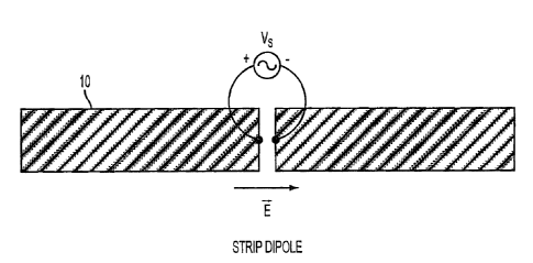
[0019] FIG. 1 is a schematic view of a dipole antenna in accordance with
the present invention;
CA 02754250 2011-09-30
[0020] FIG. 2 is a schematic view of a slot antenna in an infinite ground
plane that is complementary to the dipole of FIG. 1;
[0021] FIG. 3 is a perspective view of an apparatus in accordance with the
present invention;
[0022] FIG. 4 is a graph of the E-plane half power beamwidth for an angle
e of 35 degrees and a length L of 0 in accordance with the present invention;
[0023] FIG. 5 is a chart showing input impedance when the length L is 0 in
accordance with the present invention;
[0024] FIG. 6 is a graph of the E-plane half power beamwidth for an angle
e of 35 degrees and a length L of 0.5 inches in accordance with the present
invention;
[0025] FIG. 7 is a chart showing input impedance when the length L is 0.5
inches in accordance with the present invention;
[0026] FIG. 8 is a graph of the E-plane half power beamwidth for an angle
e of 35 degrees and a length L of 0.8 inches in accordance with the present
invention;
[0027] FIG. 9 is a chart showing input impedance when the length L is 0.8
inches in accordance with the present invention;
[0028] FIG. 10 is a graph of the E-plane half power beamwidth for an
angle e of 35 degrees and a length L of 1.2 inches in accordance with the
present invention;
[0029] FIG. 11 is a chart showing input impedance when the length L is
1.2 inches in accordance with the present invention;
6
CA 02754250 2011-09-30
[0030] FIG. 12 is a perspective view of a dipole placed over or
substantially near the center of a waveguide in accordance with the present
invention;
[0031] FIG. 13 is a side view of the dipole placed over or substantially near
the center of the waveguide in accordance with the present invention;
[0032] FIG. 14 is an exemplary view of a printed circuit board and balun
structure in accordance with the present invention; and
[0033] FIG. 15 is an enlarged view of the balun structure in accordance
with the present invention.
DESCRIPTION OF THE PREFERRED EMBODIMENTS
[0034] While this invention is susceptible of an embodiment in many
different forms, there are shown in the drawings and will be described herein
in
detail specific embodiments thereof with the understanding that the present
disclosure is to be considered as an exemplification of the principles of the
invention. It is not intended to limit the invention to the specific
illustrated
embodiments.
[0035] Embodiments of the present invention include a structure that can
provide a 120 degree E-plane half power beamwidth. Preferably, such a
structure can be easily adjusted for other beamwidths and provide high
isolation
between polarizations.
[0036] In accordance with the present invention, a dual polarized antenna
with vertical and horizontal polarizations can maintain orthogonal
polarizations
7
CA 02754250 2011-09-30
over the entire coverage sector, thus providing optimum polarization diversity
at
all sector angles. Because the elements for vertical polarization are
orthogonal
to those of the horizontal polarization, and vice versa, high isolation
between the
elements of the two polarizations can be achieved.
[0037] It is known that the E-plane beamwidth of a dipole element is
generally not sufficient to produce a horizontally polarized 120 degree half
power
beamwidth (HPBW) in a sectoral coverage antenna. However, in accordance the
present invention, a dipole element can be complimented with a slot element of
equal dimensions in a ground plane, for example, an infinite or finite ground
plane, to achieve a radiation structure with the desired E-plane half power
beamwidth.
[0038] For example, FIG. 1 is a schematic view of a dipole antenna 10 in
accordance with the present invention, and FIG. 2 is a schematic view of a
slot
antenna 20. In some embodiments, the dipole antenna 10 can be a strip dipole
antenna.
[0039] The slot antenna 20 can be complimentary to the dipole antenna 10
of FIG. 1 and, in some embodiments, the slot antenna 20 can be disposed in an
infinite ground plane 22. In embodiments of the present invention, a dominant
axis, that is, a longer axis, of the dipole 10 can be generally parallel to
the E-
plane, and a dominant axis, that is, a longer axis, of the slot 20 can be
generally
orthogonal to the E-plane.
[0040] In accordance with the present invention and applying Babinet's
Principle, if the dipole antenna 10 and the slot antenna 20 have equal
8
CA 02754250 2011-09-30
dimensions, they can produce radiation patterns, for example, far field
radiation
patterns, that are equal and have orthogonal polarizations. With the use of
the
slot radiator 20, even in a finite ground plane, a wide E-plane beamwidth can
be
achieved just as the broad H-plane beamwidth can be achieved with a dipole
radiator.
[0041] Similar to the slot antenna 20 in the infinite ground plane 22 shown
in FIG. 2, an apparatus in accordance with the present invention can include
an
open ended waveguide with appropriate surrounding structure to produce a 120
degree E-plane half power beamwidth. FIG. 3 is a perspective view of such an
apparatus 30.
[0042] As seen in FIG. 3, a waveguide 36, can be defined by a plurality of
waveguide walls 33a, 33b, 33c, 33d. In some embodiments, the waveguide 36
can be rectangular. The waveguide 36 can include a printed circuit board 31
disposed therein and can be shorted with a back plane 32. One side of each of
the waveguide walls 33a, 33b, 33c, 33d can be affixed to the back plane 32 to
define an internal dimension a of the waveguide 36, and in some embodiments,
some or all of the back plane 32 and the waveguide walls 33a, 33b, 33c, 33d
can
be metal.
[0043] In some embodiments, the first and third waveguide walls 33a, 33c
can be considered the narrow walls of the waveguide and have a length b as
shown in FIG. 3. The second and fourth waveguide walls 33b, 33d can be
considered the broad walls of the waveguide and have a length a as shown in
9
CA 02754250 2011-09-30
FIG. 3. The area a x b can be equal to a cross-section of the internal
dimension
a of the waveguide.
[0044] An E-plane probe 34 can be affixed to the printed circuit board 31
or otherwise mechanically supported within the waveguide 36 so as to excite
the
fundamental TE10 mode of the waveguide 36. The internal dimension a can
allow for propagation of the TE10 mode.
[0045] First and second adjustable plates 35a, 35b, for example metal
plates, can be adjustably attached along respective second and fourth
waveguide walls 33b, 33d, that is, the broad walls of the waveguide 36, so as
to
be disposed at an open end of the waveguide 36. A length L can include a
length along the subordinate, that is, shorter axis, of each plate 35a, 35b.
An
angle e can include an angle between either of the first or second adjustable
plates 35a, 35b and the first or third waveguide walls 33a, 33c, that is, the
narrow
waveguide walls.
[0046] In accordance with the present invention, the length L and angle e
as seen in FIG. 3 can be adjusted to produce a desired E-plane half power
beamwidth and impedance. For example, for an angle e of about 35 degrees,
the E-plane half power beamwidth can be adjusted from about 60 degrees for
L=0 to about 165 degrees for L=1.3 inches. FIGs. 4, 6, 8, and 10 are graphs
40,
60, 80, and 100, respectively of the E-plane half power beamwidth at an angle
e
of 35 degrees when L=O, 0.5, 0.8, and 1.2 inches, respectively.
[0047] FIGs. 5, 7, 9, and 11 are charts 50, 70, 90, and 110, respectively,
showing input impedance when L=O, 0.5, 0.8, and 1.2 inches, respectively. As
CA 02754250 2011-09-30
can be seen, changes to the length L can result in only small changes of the
input impedance. Thus, in accordance with the present invention, the length L
can be dynamically adjusted to vary the E-plane beamwidth without significant
impedance changes. In embodiments of the present invention, the length L can
be dynamically adjusted through an electrical and/or mechanical process.
[0048] With a waveguide in accordance with the present invention, a
dipole can be placed over or substantially near an approximate center of the
waveguide to achieve operation with dual polarizations. For example, FIGs. 12
and 13 are perspective and side views, respectively, of a dipole 120 placed
over
or substantially near the approximate center of the waveguide 36. In FIG. 12,
the
dielectric supporting structure is not shown for clarity.
[0049] As best seen in FIG. 13, the H-plane beamwidth for the dipole 120
can be varied by adjustment of the dimension h. The dimension h can include a
distance from the distal end of the first or second vertical waveguide walls
33b,
33d (the broad walls) to the conductors of the dipole 120.
[0050] In some embodiments of the present invention, the dipole 120 can
be fed with a balanced feed line (balanced microstrip) from a printed circuit
board
140 on a second side of the back plane 32. It is to be understood that the
dipole
120, the waveguide 36, and the surrounding structure of the waveguide 36 can
be disposed on a first side of the back plane 32.
[0051] FIG. 14 is an exemplary view of a printed circuit board 140 and a
balun structure 142 in accordance with the present invention. As seen in FIG.
14, the balun structure 142 can include a balun 143 and an impedance
11
CA 02754250 2011-09-30
transformer 144. The balun 143 and the impedance transformer 144 can each
be deposited on the printed circuit board 140, which, in some embodiments, can
be a feed distribution board.
[0052] The balun structure 142 can form a junction that acts as a power
divider with two path lengths of microstrip, B1 and Q. For example, FIG. 15 is
an
enlarged view of the balun structure 142 in accordance with the present
invention.
[0053] As seen in FIG. 15, the balun structure 142 can include a
connection point 150 from the balanced feed line to the dipole 120 on the
first
side of the back plane 32. In embodiments of the present invention, lengths B1
and P2 can have a 180 degree difference in electrical length from one another
to
provide proper differential feed to the balanced transmission line.
[0054] It is to be understood that waveguides and radiators as explained
and described above can be placed in an array to produce other radiation
patterns in accordance with the present invention. For example, radiation
patterns with higher directivity can be achieved by placing waveguides and
dipole
radiators in an array.
[0055] From the foregoing, it will be observed that numerous variations
and modifications may be effected without departing from the spirit and scope
of
the invention. It is to be understood that no limitation with respect to the
specific
system or method illustrated herein is intended or should be inferred. It is,
of
course, intended to cover by the appended claims all such modifications as
fall
within the spirit and scope of the claims.
12