Note: Descriptions are shown in the official language in which they were submitted.
CA 02754571 2016-10-17
=
A METHOD AND SYSTEM FOR DIGITAL NARROWBAND, WAVELENGTH
SPECIFIC COOKING, CURING, FOOD PREPARATION, AND PROCESSING
[0001] This application claims priority to and is based on U.S. Provisional
Application
No. 61/157,799, filed on March 5, 2009.
BACKGROUND OF THE INVENTION
[0002] Many different types of cooking have been performed for thousands of
years
by way of a variety of broadband heating sources. The earliest and most
fundamental
heating source widely used by man for heating was fire. It produces radiant
heat energy
which ranges from the UV to the long infrared. The actual shape of the output
curve,
which defines the strength of the radiation at each wavelength, changes as a
function of
the temperature of the fire. As wood and coal fires gave way to oil and gas
fired ovens
or cooking surfaces, the fundamentals stayed the same in that the combustion
of the
fire produced a broadband source of radiant energy. A knowledge base built up
wrapped around the assumption of the commonly available broadband equipped
oven
cooking. As electricity became more commonplace in the early 20th century,
electrically
energized resistance based heating coils were often used instead of the
various
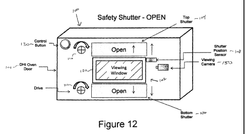
combustion-based sources. These resistance heating coils are often generically
referred to in the industry as Calrods. Although they seemed new and modern to
the
consumer, they were still fundamentally very broadband irradiation sources.
This is well
known but is evidenced by the fact that a Calrod heating coil may glow bright
red, which
indicates output in the visible spectrum and will also produce energy
continuously well
out into the long infrared wavelengths. Although it is a very broadband output
source, its
peak output, depending on at what temperature it is operated, is typically in
the long
infrared category.
[0003] In the last
several decades, quartz halogen lamps, tubes, and bulbs have
been used in various types of oven or curing applications as well. Because the
quartz
1
CA 02754571 2011-09-06
WO 2010/102261 PCT/US2010/026438
approximates a much hotter blackbody Planckian source, it outputs
substantially more
energy in the visible spectrum than typical resistance heat sources. Different
quartz
lamps are designed to run at different temperatures which changes the center
of its
output curve, also affecting how much visible light energy it produces. The
center or
peak output is typically in the near infrared or middle infrared ranges.
Regardless of the
temperature at which they are operated, quartz is still a broadband source
which has its
peak output in the near to mid infrared range and with a bandwidth of several
thousand
nanometers.
[0004] Even tungsten filament incandescent light bulbs have been used as
cooking
heat sources for specialized ovens. Franklin S. Malick, in his U.S. Patent No.
4,481,405,
teaches a simple system which uses incandescent light bulbs to cook food that
is in
plastic cooking pouches. While quartz is a more unusual and specialized oven
than
simple resistance coils or burners, it is clearly broadband analog irradiation
devices that
are being used as the sources.
[0005] Various combinations of these modalities have been used but all of
them
simply combine broadband analog devices in different ways. Robert A.
Mittelsteadt in
his U.S. Patent No. 4,486,639 teaches one of the earlier multimode cooking
methodologies. He teaches the combination of a microwave oven with quartz lamp
heating devices. By having a control option of using the quartz lamps to
either directly
irradiate or to heat the air and then cook by hot air convection, he combines
three
different functionalities into a single oven. Although microwave cooking is
probably the
newest fundamentally different cooking technology, the fundamental radio
frequency
microwaves at its heart are actually a much broader bandwidth analog source
than the
ones mentioned above. In fact, the only cooking devices that have been
available in the
marketplace prior to this invention are analog broadband types.
[0006] Ronald Lentz et al. understood and re-taught some fundamental
concepts in
their U.S. Patent No. 5,382,441. They recognize that long wavelength infrared
has less
penetration depth with food than shorter wavelengths. They also recognize and
re-
taught at some depth the classic physics of Planck's law of blackbody's which
describes
the broadband radiation output which changes as a function of temperature of
the
heating device. They recognize that, while they would like to be able to
control the
2
CA 02754571 2011-09-06
WO 2010/102261 PCT/1JS2010/026438
wavelengths of output, they do not have an elegant, direct, or efficient
solution to this
problem. They absolutely cannot do it efficiently. They therefore teach using
a
broadband analog source and superimposing a filter between the radiation
source and
the food to be cooked. They suggest either a water filter or a treated glass
filter. They
recognize that even their best choice of a quartz lamp ". . . has been
determined to
deliver at most 35% of its radiation between 800 and 1300 nm . . .". By
teaching the
use of a filter they are therefore going to be throwing away 65% of their
energy. That
65% will be absorbed by a filter and will result in either superheating the
filter and thus
turning it into its own blackbody radiator, or using some external means to
remove the
heat from the filtration means. This is cumbersome to implement. Under either
circumstance it is a highly inefficient way of eliminating the unwanted
wavelengths from
a broadband analog source. While they are teaching limiting the irradiation
that reaches
the target to approximately 500 nm of bandwidth, it still represents a
broadband source.
They fail to teach a high-resolution absorption curve. They therefore fail to
teach or
recognize that there are micro-peaks and micro-troughs in many products'
absorption
curves which their inefficient technique will still be incapable of
addressing. For
example the present invention can take advantage of the fact that; a high-
resolution
curve indicates pizza dough is roughly four times more absorptive at 1200 nm
than it is
at 900 nm. The same dough is about three times more absorptive at 1200 nm than
it is
at 1100 nm. Lentz fails to teach any kind of solution which would take
advantage of this
important data to optimize the cooking way beyond what their solution can
provide.
They also fail to teach a digital semi-conductor based narrowband source or
how one
would build or implement same. They also fail to teach what a narrowband
source
would bring as advantages. They also fail to teach and did not invent any
"instant on" /
"instant off' technology. They neither fail to teach any pulsed irradiation
technology nor
what the advantages would be. While they casually mentioned that their
invention could
be practiced with other IR radiation sources, none of them are described as
digital or
semiconductor-based or narrowband or directional. They further fail to teach a
methodology for implementing any IR irradiation sources that accomplish direct
electron
to photon conversion. Clearly the thrust of their invention is comprised of
using a filter to
reduce or eliminate some unwanted broadband range.
3
CA 02754571 2011-09-06
WO 2010/102261 PCT/US2010/026438
[0007] Much of a fundamental concept has been generally understood
for years, that
the wavelength of irradiation has various effects on cooking. It is generally
understood,
for example, that very long wavelengths contribute to skin absorption or
heating the
target food very near the surface. This is why most current ovens typically
are designed
to not expose the food directly to the irradiation of long infrared sources
unless surface
heating is the desired end result. Broiler heating elements are typically
mounted above
the food to be cooked so that they can directly irradiate it, thus searing and
cooking
near the surface. Baking heating elements are, on the other hand, mounted
below the
food such that the pan or cooking vessel is between the food and the heating
element
so the food will not be directly irradiated by the longwave infrared energy.
Another
example of this concept is taught by David McCarter in U.S. Patent No.
6,294,769 which
is an infrared device for keeping food warm and ready to eat. Specifically, it
describes a
system that is useful for keeping foods, such as French fries, at a desirable
temperature
= without resulting in substantial additional internal cooking. The concept
being taught is
one of using a resistive broadband ceramic heating element which produces
infrared
heat largely in the wavelength range from 7.91 to 4.7 p. Figure 1 shows his
absorption
graph of French fries which generally shows an increasing absorption with
longer
wavelengths up to a peak absorption at about 5.4 p and then a sloped off
absorption to
the maximum wavelength shown on the graph at 7 p. The specific absorption
coefficient
for French fries varies from about 62% at 4.7 p to about 95% at 5.4 p and then
backs
down to about 73% at 7 p. What McCarter fails to teach is the use of
narrowband
energy and a digital source which would facilitate a precise matching of the
irradiation
wavelength to the exact absorption coefficient that was desired for the
application. In
the broadband arrangement that McCarter describes, the French fries exhibited
50%
more absorption at one wavelength compared to a wavelength only 700 nm away.
By
using the narrowest source that he was able to find, he was not able to tune
in to the
absorption that would have been ideal. It is not possible with broadband
sources. He
also fails to teach a digital heating system which can be turned off and on
instantly to
maintain the food at the exact right temperature but with substantial energy
savings by
having a reduced duty cycle, since energy is only being consumed when the
heating
devices are turned on. He shows a very low resolution graph which was adequate
for
4
CA 02754571 2011-09-06
WO 2010/102261 PCT/1JS2010/026438
his purpose. However, because it lacks the resolution which would have
provided the
detailed absorption curve shapes, he can not and does not teach that it may be
possible
to get the same average absorption at a much shorter wavelength if it were
possible to
irradiate with a narrowband system which irradiates into a localized, micro-
peak rather
than a global peak.
[0008] Yang Kyeong Kim et al. taught in U.S. Patent No. 6,348,676 a
methodology
for using quartz lamps for cooking. They teach, as was mentioned earlier, that
the
shape of the output curve can be varied as a function of what temperature the
lamp is
designed to function at. They show a quartz lamp which is designed to function
as a
2400 K. device has its peak output at approximately 1.1 p. By comparison, a
2300 K.
device has its peak output at approximately 1.25 ii with a somewhat flatter
output curve.
Regardless of the wavelength of maximum output, the curves for both devices
are
shown to have substantial output throughout the visible range and out to 3 p
or more in
the mid infrared region. In Figure 2, Kim shows the absorption spectral curves
for
different food items. While they are low resolution absorption curves, each
curve is
unique and different from all the others. What they generally have in common
is
substantially more transmission (less absorption) below about 1400 nm than
above that
wavelength. Kim tries to make the case that by using a quartz lamp with a
lower color
temperature, it is possible to cook the food faster because of higher output
of longer
wavelength infrared energy which will be in the generally higher absorption
region,
which is shown to be generally above about 1400 nm. What Kim et al. fail to
teach is
how to take advantage of the optimal cooking absorptions of the individual
food items.
Again, the food items have local, micro-peaks and micro-troughs in their
absorption
curves which are substantially different from one another. Substantial
differences are
evident even within less than 100 nm of wavelength. It is apparent that those
small
features were not meaningful to Kim and cohorts because the graph that is
shown has
very little resolution or detail. It is obvious by studying the broadband
shape of the
curves shown in Figure 2 that it would not be possible to irradiate and take
advantage of
wavelength matching any of the micro-peaks or micro-troughs that may be
characteristic of a certain food product. Similar to McCarter, they totally
fail to teach a
CA 02754571 2011-09-06
WO 2010/102261 PCT/US2010/026438
methodology for cooking with digital, narrowband irradiation to truly optimize
the
cooking opportunities and efficiencies.
[0009] Brian Farkas et al. in U.S. Patent No. 7,307,243 teach yet other
ways of
incorporating a mix of broadband sources. They also recognized that longer
wavelengths are generally absorbed closer to the surface of food items and
conversely,
that shorter wavelengths tend to have a greater penetration. They teach the
use of
Planckian, blackbody sources at different wattages and temperatures. They show
by
way of several graphs how these conventional analog broadband sources can be
changed in terms of central wavelength and flatness of curve. They again show
what is
well known in physics, that the hotter a blackbody source is operated, the
shorter the
center wavelength will be. Correspondingly, as the wavelength grows shorter,
the curve
becomes somewhat steeper and more abrupt. It is again shown however that no
matter
how many different ways it is applied, it is still an analog broadband source
of several
thousand nanometers in width and whose steepness and curve changes
proportional to
applied voltage or current (wattage). They further recognize that the body and
structure
of the oven itself heats up over a period of time and becomes its own
blackbody re-
radiator. They teach and show that even when the heating elements are turned
off there
is still substantial radiant cooking that is being done in the oven as a
result of the
structural re-radiation. This teaches directly away from the current invention
which has
the ability to turn on and off instantly and warm-up time has virtually no
effect on the
quality of the cooking. Farkas continues to teach what has been known for many
years
but just in a differently configured oven arrangement. Farkas, like the others
mentioned
earlier, fails to teach any of the advantages that would be gained from the
present
invention that incorporates digital narrowband sources to take advantage of
the micro-
peaks and micro-valleys in the high-resolution absorption curves to optimize
the desired
heating or cooking. They also fail to teach the additional speed of cooking
that is
possible by using direct narrowband irradiation that is properly matched to
the target
and cooking duties.
[0010] Various other patents teach novel ways of controlling or turning the
traditional
analog broadband sources up or down or changing their distance from the
cooking
target. Donald Pettibone and cohorts with their U.S. Patent No. 5,883,362 is
an example
6
CA 02754571 2011-09-06
WO 2010/102261 PCT/US2010/026438
of such a patent but it also fails to teach any of the advantages, techniques,
and
technology that the present invention does.
SUMMARY OF THE INVENTION
[0011] The subject invention provides for the implementation of small or
substantial
quantities of infrared radiation devices that are highly wavelength selectable
and can
facilitate the use of infrared radiation for whole new classes of cooking
applications and
techniques that have not been available historically.
[0012] An object of this invention is to provide an oven, process, or
treatment system
with a thermal IR heating system possessing improved IR energy conversion
efficiency
performance.
[0013] Another object of this invention is to provide an IR heating system
having IR
penetration depth performance tuned to the particular absorption spectrum of
the
specific material being cooked, processed, or targeted.
[0014] Another object of this invention is to provide a thermal IR
radiation system
which can incorporate an engineered mixture of REDs which produce IR radiation
at
such selected narrow wavelength bands as may be optimal for classes of cooking
applications.
[0015] Another object of this invention is to provide an IR heating system
capable of
being driven in a pulsed mode; said pulsed mode being particularly suited to
providing
IR heat to food items as they are transported during the cooking process or to
facilitate
synchronous tracking of the food items.
[0016] Another object of this invention is to provide IR heating elements
that are
more directable via metalized reflector elements.
[0017] Another object of this invention is to provide an IR heating system
capable of
working in conjunction with a food temperature measurement system to provide
food-
specific IR heating capability.
[0018] Another object of this invention is to provide IR heating elements
that are
fabricated as arrays of direct current-to-photon IR semiconductor based
emitters or
radiance emitting diodes (REDs).
7
CA 02754571 2011-09-06
WO 2010/102261 PCIYUS2010/026438
[0019] Yet another
advantage of this invention is to provide a heat injection system
utilizing digital narrowband semiconductor-based devices fabricated into
arrays using at
least one of heat conductive circuit board mounted devices, chip-on-board
mounted
devices, ball grid array mounted devices, enlarged sized devices, and
integrated circuit
based of devices.
[0020] Yet another
advantage of this invention is to provide an infrared irradiation
system of substantial radiant output at highly specific single or multiple
narrow
wavelength bands.
[0021] Yet another
advantage of this invention is the functionality to produce
powerful, thermal infrared radiation and to be highly programmable for at
least one of
position, intensity, wavelength, turn-on/turn-off rates, directionality,
pulsing frequency,
and product tracking.
[0022] Yet another
advantage of the invention is the facilitation of a more input
energy efficient methodology for injecting heat energy compared to current
broadband
sources.
[0023] Yet another
object of this invention is to provide a general radiant heating
system for a wide range of applications to which it can be adapted to provide
the
increased functionality of wavelength selective infrared radiation in
combination with the
programmability and pulsing capability.
[0024] Yet another
advantage of this invention is the ability to facilitate extremely fast
high intensity burst pulses with much higher instantaneous intensity than
steady state
intensity. Pulsing can also facilitate a higher energy instantaneous optical
impulse which
can achieve a greater level of penetration depth which may be important for
some
applications.
[0025] Yet another
advantage of the invention is that it can be modularly scaled as
required with the narrowband semiconductor-based devices to incorporate
whatever
number of devices may need to be arrayed together to provide the necessary
power,
size, configuration, geometry, wavelength combinations, or other aspects
dictated by
the engineering for a particular application. Arrays of
these devices may include
dozens hundreds or thousands of them as required to meet the specific
application.
8
CA 02754571 2011-09-06
WO 2010/102261 PCT1US2010/026438
[0026] Yet another advantage of the invention is that waste heat can be easily
conducted away to another location where it is needed or can be conducted out
of the
using environment to reduce non-target heating.
[0027] Yet another
advantage of the invention is the ability to build an oven or target
heating system whose ambient waste heat can be easily removed from the
immediate
vicinity of the digital narrowband semiconductor devices and transferred to a
preferred
location which may even be an outdoor location.
[0028] Yet another advantage of the invention is that the RED devices can be
packaged in high density to yield solid state, thermal IR output power levels
that have
heretofore not been practically attainable.
[0029] In one
aspect of the presently described embodiments, the system comprises
an irradiation zone into which a food item can be located for at least one of
direct or
indirect irradiation, a structure for holding directional irradiation devices
proximate an
irradiation zone such that the irradiation from the irradiation device can
either directly or
indirectly impact the food item, at least one narrowband, semi-conductor-based
radiation emitting device operative to selectively emit at least one narrow
band of
radiation, the at least one narrowband, semi-conductor-based radiation
emitting device
being a digital device such that it has a very narrow range of voltage change
at its turn-
on threshold, and the at least one narrowband device being selected based on
an
irradiation output wavelength that matches an absorption characteristic of at
least one
food item, and, a control system which at least supplies electrical current to
operate the
narrowband irradiation devices.
[0030] In another
aspect of the presently described embodiments, the system further
comprises a viewing window positioned to allow viewing of the irradiation zone
without
passing the irradiation output wavelength.
[0031] In another
aspect of the presently described embodiments, the system further
comprises a shutter system to selectively turn off radiation during viewing.
[0032] In another
aspect of the presently described embodiments, the system further
comprises at least one door operative to contain the irradiation output
wavelength in the
system.
9
CA 02754571 2011-09-06
WO 2019/102261 PCT/US2010/026438
[0033] In another aspect of the presently described embodiments, the system
further
comprises sensors operative to sense position of the food items.
[0034] In another aspect of the presently described embodiments, the
sensors
comprise a camera that senses the position of the food item, type of food, and
size of
the food item.
[0035] In another aspect of the presently described embodiments, the camera
is an
infrared camera.
[0036] In another aspect of the presently described embodiments, output of
the
sensors is used to determine a status of containment.
[0037] In another aspect of the presently described embodiments, the system
further
comprises a conveyor system to transport the food items into the irradiation
zone.
[0038] In another aspect of the presently described embodiments, the system
further
comprises sensors operative to sense at least one aspect about the food item
at least
one of before, during, or after the irradiation and take action as a result of
the sensing.
[0039] In another aspect of the presently described embodiments, the
sensors
comprise a camera that senses position, type of food, and size of the food
item.
[0040] In another aspect of the presently described embodiments, the camera
is an
infrared camera.
[0041] In another aspect of the presently described embodiments, the at
least one
aspect is temperature, surface dryness, color, or size.
[0042] In another aspect of the presently described embodiments, the
narrowband
irradiation device produces its narrowband irradiation in the near infra-red
range
somewhere between 700nm and 1200nm.
[0043] In another aspect of the presently described embodiments, the
narrowband
irradiation device produces at least one narrowband irradiation band in the
mid infra-red
range between 1200nm and 3500nm.
[0044] In another aspect of the presently described embodiments, the
narrowband
irradiation device produces at least one narrowband irradiation band in the
visible light
range.
[0045] In another aspect of the presently described embodiments, the
narrowband
irradiation device produces at least one narrowband irradiation band above
3500 nm.
CA 02754571 2011-09-06
WO 2010/102261 PCT/US2010/026438
[0046] In another aspect of the presently described embodiments, the at
least one
narrowband semi-conductor-based radiation emitting device produces its
narrowband
irradiation at two different narrowband irradiation wavelengths each of which
is chosen
such that the wavelength matches an absorption characteristic of an
anticipated target
which may be irradiated.
[0047] In another aspect of the presently described embodiments, the
absorption
characteristics of the food items are different at the center of each of the
two
wavelengths.
[0048] In another aspect of the presently described embodiments, the system
further
comprises broadband irradiating elements to be selectively activated for
cooking the
food item in addition to narrowband heating.
[0049] In another aspect of the presently described embodiments, the
broadband
irradiating elements comprise at least one of quartz layers, sensitive heating
elements
and microwave elements.
[0050] In another aspect of the presently described embodiments, the system
uses
at least two (2) irradiation bands, one of which is below 1400 nm and the
other of which
is above 1400 nm.
[0051] In another aspect of the presently described embodiments, the system
comprises a cooking chamber with a configuration to safely contain irradiated
energy
there within and into which a food item can be located for at least one of
direct or
indirect irradiation, a structure for at least partially enclosing the cooking
chamber and
for holding directional irradiation devices proximate to the cooking zone such
that the
irradiation from the irradiation devices can at least one of directly or
indirectly impact the
food item, at least one narrowband, semi-conductor-based, emitting device, the
at least
one narrowband, semi-conductor-based emitting device being chosen such that
the
wavelength of its irradiation output matches at least one absorption
characteristic at that
wavelength of at least one of the target food items, and, a control system for
supplying
at least the electrical current to digitally control the narrowband
irradiation devices to
provide the irradiation output in the chamber based on at least one of user
interface
settings, sensor output, or a determination that the chamber is active and
safely
containing the irradiated energy.
11
CA 02754571 2011-09-06
WO 2010/102261 PCT/US2010/026438
[0052] In another aspect of the presently described embodiments, the system
further
comprises a viewing window positioned to allow viewing of the irradiation zone
without
passing the irradiation output wavelength.
[0053] In another aspect of the presently described embodiments, the system
further
comprises a shutter system to selectively turn off radiation during viewing.
[0054] In another aspect of the presently described embodiments, the system
further comprises a conveyor system to transport the food items into the
irradiation
zone.
[0055] In another aspect of the presently described embodiments, the system
further comprises sensors operative to sense at least one aspect about the
food item at
least one of before, during, or after the irradiation and take action as a
result of the
sensing.
[0056] In another aspect of the presently described embodiments, the
sensors
comprise a camera that senses position, type of food, and size of the food
item.
[0057] In another aspect of the presently described embodiments, the camera
is an
infrared camera.
[0058] In another aspect of the presently described embodiments, the at
least one
aspect is temperature, surface dryness, color, or size.
[0059] In another aspect of the presently described embodiments, the
narrowband
irradiation device produces its narrowband irradiation in the near infra-red
range
somewhere between 700nm and 1200nm.
[0060] In another aspect of the presently described embodiments, the
narrowband
irradiation device produces at least one narrowband irradiation band in the
mid infra-red
range between 1200nm and 3500nm.
[0061] In another aspect of the presently described embodiments, the
narrowband
irradiation device produces at least one narrowband irradiation band in the
visible light
range.
[0062] In another aspect of the presently described embodiments, the
narrowband
irradiation device produces at least one narrowband irradiation band above
3500 nm.
[0063] In another aspect of the presently described embodiments, the at
least one
narrowband semi-conductor-based radiation emitting device produces its
narrowband
12
CA 02754571 2011-09-06
WO 2010/102261 PCT/US2010/026438
irradiation at two different narrowband irradiation wavelengths each of which
is chosen
such that the wavelength matches an absorption characteristic of an
anticipated target
which may be irradiated.
[0064] In another aspect of the presently described embodiments, the
absorption
characteristics of the food items are different at the center of each of the
two
wavelengths.
[0065] In another aspect of the presently described embodiments, the system
further
comprises broadband irradiating elements to be selectively activated for
cooking the
food item in addition to narrowband heating.
[0066] In another aspect of the presently described embodiments, the
broadband
irradiating elements comprise at least one of quartz layers, sensitive heating
elements
and microwave elements.
[0067] In another aspect of the presently described embodiments, the system
uses
at least two (2) irradiation bands, one of which is below 1400 nm and the
other of which
is above 1400 nm.
[0068] In another aspect of the presently described embodiments, the
control system
comprises a cooling system operative to cool system electronics.
[0069] In another aspect of the presently described embodiments, the system
further
comprises a notification system operative to alert a user of a cooking or
system status.
[0070] In another aspect of the presently described embodiments, the system
further
comprises a ventilation system operative to clear the cooling chamber of at
least one of
humidity, fumes or vapor.
[0071] In another aspect of the presently described embodiments, the
ventilation
system comprises a fan or a catalyst.
[0072] In another aspect of the presently described embodiments, the method
comprises introducing at least one target food item into the irradiation zone
and
positioning it such that it can be either directly or indirectly irradiated by
the radiation
emitting devices, safely containing the irradiation zone, emitting directional
radiation
from at least one digital narrowband, semi-conductor-based irradiation device
during
periods when the irradiation zone is safely contained, and, irradiating the at
least one
13
CA 02754571 2011-09-06
WO 2010/102261 PCT/US2010/026438
food item with at least one narrowband wavelength which matches an absorptive
characteristic of the at least one targeted food item during the emitting.
[0073] In another aspect of the presently described embodiments, the
irradiating the
at least one food item comprises painting the at least one food item as a
function of the
direction emitting.
[0074] In another aspect of the presently described embodiments, the method
further
comprises irradiating an element to add a selected flavor to the at least one
food item.
[0075] In another aspect of the presently described embodiments, the
emitting
comprises pulsing the at least one irradiation device.
[0076] In another aspect of the presently described embodiments, the at
least one
narrowband wavelength comprises two wavelength bands selected based on
substantially different absorption characteristics at each center of the
wavelength
bands.
[0077] In another aspect of the presently described embodiments, centers of
the
selected wavelength bands are separated by at least 150 nm.
[0078] In another aspect of the presently described embodiments, the at
least one
narrowband wavelength achieves deep penetration into the food item.
[0079] In another aspect of the presently described embodiments, the at
least one
narrowband wavelength achieves surface heating of the food item.
[0080] In another aspect of the presently described embodiments, the at
least one
narrowband wavelength achieves deep penetration of the food item without
heating the
surface of the food item.
[0081] In another aspect of the presently described embodiments, the method
further
comprises irradiating the at least one food item using a broadband source.
[0082] In another aspect of the presently described embodiments, the
irradiating
achieves both deep penetration of the food item and surface browning of the
food item.
[0083] In another aspect of the presently described embodiments, the method
comprises arranging for a food item to be cooked, cured, or dried to be in an
irradiation
zone which is proximate to at least one narrowband, semi-conductor band
radiation
emitter, irradiating the food item for a period of time from the at least one
digital
narrowband, semi-conductor-based radiation emitter device at a wavelength
which
14
corresponds to a preferred absorption characteristic of the food item at that
wavelength,
and, controlling the irradiating by sensing at least one aspect of the food
item at least
one of before. during, or after the Irradiation and taking action as a result
of the sensing.
[1301341 In another
aspect of the presently described embodiments, the method
comprises transporting the food item into a cooking chamber, sensing a
position of the
food item as the food Item is being transported into the cooking chamber,
detecting that
the food item is in a desired position, ceasing the transporting based on the
detecting,
closing the cooking chamber to safely contain contents of the chamber, sensing
or
inputting aspects of the food item, determining a cooking pattern based on the
sensing
or inputting and based on cooking parameters, irradiating the food item based
on the
cooking pattern for a period of time from at least one digital narrowband,
semiconductor-
based radiation emitter device at a wavelength which corresponds to a
preferred
absorption characteristic of the food item at that wavelength, opening the
cooking
chamber after completion of the irradiating, and, transporting the food Item
out of the
cooking chamber.
[0084a] In another aspect of the presently described embodiments, there is
provided
a processing system for heating food, the system comprising: a cooking chamber
with a
configuration to safely contain irradiated energy there within and into which
a food item
can be located for irradiation; a structure for at least partially enclosing
the cooking
chamber and for holding directional irradiation devices proximate to the
cooking zone
such that the irradiation from the irradiation devices is emitted directly
from the
irradiation devices to impact the food item in the cooking chamber; the
Irradiation
devices comprising at least one narrowband, semi-conductor-based, emitting
device,
the at least one narrowband, semi-conductor-based emitting device being chosen
such
that the wavelength of its irradiation output matches at least one absorption
characteristic at that wavelength of at least one of the target food items;
and, a control
system for supplying at least the electrical current to digitally control the
narrowband
irradiation devices to provide the irradiation output in lhe chamber based on
1) at least
one of user interface settings or sensor output, and 2) a determination that
the cooking
chamber is active and safely containing the irradiated energy, to irradiate
the food (tern
for a period of time when the cooking chamber Is active and closed, using at
least a
door to prevent non-visible Infrared energy from reaching an outside viewer or
observer.
16
CA 2754571 2019-06-13
1[0084b1 In another aspect of the presently described embodiments, there Is
provided
a method for cooking, drying, or curing a food Item, the method comprising:
Introducing
at least one target food item into an irradiation zone and positioning it such
that It can be
irradiated; safely containing the irradiation zone; emitting directional
radiation from at
least one digital narrowband, semi-conductor-based irradiation device during
periods
when the irradiation zone is safely contained based on 1) at least one of user
interface
settings or sensor output, and 2) a determination that the irradiation zone is
active and
closed, using at least a door to prevent non-visible infrared energy from
reaching an
outside viewer or observer, thereby safely containing the Irradiated energy;
and,
Irradiating the at least one food item with at least one narrowband wavelength
which
matches an absorptive characteristic of the at least one targeted food item
during the
emitting.
[0084c] In another aspect of the presently described embodiments, there is
provided
a method for processing a food item, the method comprising: transporting the
food item
into a cooking chamber; sensing a position of the food item as the food item
is being
transported into the cooking chamber; detecting that the food Item is in a
desired
position; ceasing the transporting based on the detecting; closing the cooking
chamber
to safely contain contents of the chamber; sensing or inputting aspects of the
food item;
determining a cooking pattern based on the sensing or inputting and based on
cooking
parameters; irradiating the food item for a period of time when the cooking
chamber is
safely closed from at least one digital narrowband, semi-conductor-based
radiation
emitter device at a wavelength which corresponds to a preferred absorption
characteristic of the food item at that wavelength based on the cooking
pattern and a
determination that the chamber is active and safely containing the irradiated
energy;
opening the cooking chamber after completion of the irradiating; and,
transporting the
food item out of the cooking chamber,
[0024d] In another aspect of the presently described embodiments, there is
provided
a processing system for heating food, the system comprising: a cooking chamber
with a
configuration to safely contain irradiated non-visible infrared energy there
within and into
which a food Item can be located for Irradiation; a structure for at least
partially
enclosing the cooking chamber and for holding directional Irradiation devices
proximate
to the cooking zone such that the irradiation from the irradiation devices can
Impact the
food item; the irradiation devices comprising at least one narrowband, semi-
conductor-
based, non-visible infrared emitting device, the at least one narrowband, semi-
conductor-based non-visible Infrared emitting device being chosen such that
the
16a
CA 2754571 2019-06-13
wavelength of its non-visible infrared irradiation output matches at least one
absorption
characteristic at that wavelength of at least one of the target food Items; a
control
system for supplying at least the electrical current to digitally control the
narrowband
irradiation devices to provide the non-visible infrared Irradiation output in
the chamber
based on at least one of user interface settings, sensor output, or a
determination that
the chamber is active and safely containing the non-visible infrared
irradiated energy;
and one or more of: a filtration window incorporating a visible pass filter to
allow only
visible light to reach a viewer, a reflective viewing path configured such
that only visible
light Is reflected through a viewing pass to the viewer, and a camera and
display to view
the inside of the cooking chamber.
BRIEF DESCRIPTION OF THE DRAWINGS
[0005] Figure 1 is a graph showing an absorption curve;
[0080] Figure 2 is a graph showing an absorption curve;
[0087] Figure 3 is an illustration of a narrow band emitting device;
[001381 Figure 4 is an illustration of a narrow band emitting device;
[0059] Figure 5 Is an Illustrabon of a narrow band emitting device:
[0090] Figure 6 Is an illustration of a narrow band emitting device;
[0091] Figure 7 is an illustration of a narrow band emitting device;
[0092] Figure 8 Is an Illustration of a narrow band emitting device;
[0093] Figure 9 Is an illustration of a narrow band emitting device;
[0094] Figure 10 is an Illustration of an array of narrow band
emitting devices;
[0095] Figure 11 Is a graph showing an absorption curve;
10096] Figure 12 is an illustration of an embodiment of the presently
described
embodiments;
15b
CA 2754571 2019-06-13
CA 02754571 2011-09-06
WO 2010/102261 PCMS2010/026438
[0097] Figure 13 is an illustration of an embodiment of the presently
described
embodiments;
[0098] Figure 14 is an illustration of an embodiment of the presently
described
embodiments;
[0099] Figure 15 is a graph illustrating operation of "instant on" devices
versus
resistive heating devices; and,
[00100] Figure 16 is a chart showing absorption versus transmission.
DETAILED DESCRIPTION
[00101] This invention disclosure covers a system for direct injection of
digital,
narrowband wavelength specific thermal-infrared (IR) energy into foods and
other
target items for a range of heating, cooking, processing, and curing
applications
including the various types of cooking preparations appropriate for bread,
pastries,
packages, individual recipe components, pizza, meat, seafood, poultry,
vegetables, pre-
prepared foods or meals, portions or combinations thereof, or various other
heating
processes. The purpose for practicing this invention may include heating,
raising or
maintaining the temperature of food or other items to cause cooking, baking,
frying,
proofing, browning, warming, fermenting, curing, and drying, as well as other
reactions
involved in the manufacturing or preparation of foods or other products. The
invention is
especially applicable to operations that require or will benefit from the
implementation of
digital semi-conductor based narrowband irradiation at specifically selected
wavelengths by way of directing, pulsing, or injecting the radiant photonic
energy. This
new system is particularly advantageous when an application requires at least
one of
high-speed, high performance, high selectivity, or high energy efficiency
which may vary
as the invention is applied to different applications.
[00102] With respect to narrowband radiation, the benefits of providing
wavelength
specific irradiation can be illustrated by looking at a hypothetical radiant
heating
example. Assume that a material which is generally transparent to
electromagnetic
radiation from the visible range through the mid-infrared range requires
process heating
to support some manufacturing operation. The examples described above are
representative of how the presently described embodiments might be most
16
CA 02754571 2011-09-06
WO 2010/102261 PCT1US2010/026438
advantageously applied for real applications. The ability to generate only
wavelength-
specific radiant energy output as described within this disclosure holds the
promise of
greatly improving the efficiency of various process heating applications, for
example, for
heating, curing or drying food items.
[00103] This invention is directly related to a novel and new approach to be
able to
directly output substantial quantities of radiation at selected wavelengths
for the
purpose of replacing such analog broadband type heating devices, e.g. for food
processing.
[00104] It is also noted that recent advances in semiconductor processing
technology
have resulted in the availability of direct electron-to-photon solid-state
emitters that
operate in the general near infrared and mid-infrared ranges. Some of these
solid state
devices operate analogous to common light emitting diodes (LEDs), only they do
not
emit visible light but emit true, thermal IR energy at the longer near
infrared and mid-
infrared wavelengths. Some of the first of these that became available
represent an
entirely new class of devices which utilize quantum dot technology that have
broken
through the barriers which have prevented useable, cost effective solid state
devices
from being produced which could function as direct electron to photon
converters whose
output is pseudo-monochromatic and in the mid-infrared wavelength band.
[00105] To distinguish this new class of devices from the conventional shorter
wavelength devices (LEDs), these devices are more appropriately described as
radiance or radiation emitting diodes (REDs). The devices have the property of
emitting
radiant electromagnetic energy in a tightly limited wavelength range.
Furthermore,
through proper semiconductor processing operations, REDs can be tuned to emit
at
specific wavelengths that are most advantageous to a particular radiant
treatment
application by matching the target's absorption spectrum accordingly.
[00106] In addition, innovations in RED technology related to the formation of
a doped
planar region in contact with an oppositely doped region formed as a randomly
distributed array of small areas of material or quantum dots for generating
photons in
the targeted IR range and potentially beyond has evolved. This method of
fabrication,
or others such as the development of novel semiconductor compounds, adequately
applied would yield suitable pseudo-monochromatic, solid-state mid-infrared
emitters for
17
the subject invention. Alternate semi-conductor technologies may also become
available in both the mid-infrared as well as for long wavelength infrared
that would be
suitable building blocks with which to practice this invention.
[00107] Direct electron (or electric current)-to-photon conversions as
contemplated
within these described embodiments occur within a narrow wavelength range
often
referred to as pseudo-monochromatic, consistent with the intrinsic band-gap
and
quantum dot geometry of this fabricated diode emitter. It is anticipated that
the half-
power bandwidths of candidate RED emitters will fall somewhere within the 20-
500
nanometer range. The narrow width of infrared emitters of this type should
support a
variety of wavelength-specific irradiation applications as identified within
the content of
this complete disclosure. One family of RED devices and the technology with
which to
make them are subject of a separate patent application, U.S. Application
Serial No.
60/628,330, filed on November 16, 2004, entitled "Quantum Dot Semiconductor
Device" and naming Samar Sinharoy and Dave Wilt as inventors (Attorney Docket
No.
ERI.P.US0002; Express Mail Label No. EL 726091609 US) (also filed as U.S.
Application Serial No. 11/280,509 on November 16, 2005).
[00108] According to this "Quantum Dot Semiconductor Device"
application,
semiconductor devices are known in the art. They are employed in photovoltaic
cells
that convert electromagnetic radiation to electricity. These devices can also
be
employed as light emitting diodes (LEDs), which convert electrical energy into
electromagnetic radiation (e.g., light). For most semiconductor applications,
a desired
bandgap (electron volts) or a desired wavelength (microns) is targeted, and
the
semiconductor is prepared in a manner such that it can meet that desired
bandgap
range or wavelength range.
[00109] The ability to achieve a particular wavelength of emission or
electron volt of
energy is not trivial. Indeed, the semiconductor is limited by the selection
of particular
materials, their energy gap, their lattice constant, and their inherent
emission
capabilities. One technique that has been employed to tailor the semiconductor
device
is to employ binary or tertiary compounds. By varying the compositional
characteristics
of the device, technologically useful devices have been engineered.
18
CA 2754571 2020-03-17
CA 02754571 2011-09-06
WO 2010/102261 PCT/US2010/026438
[00110] The design of the semiconductor device can also be manipulated to
tailor the
behavior of the device. In one example, quantum dots can be included within
the
semiconductor device. These dots are believed to quantum confine carriers and
thereby alter the energy of photon emission compared to a bulk sample of the
same
semiconductor. For example, U.S. Patent No. 6,507,042 teaches semiconductor
devices including a quantum dot layer. Specifically, it teaches quantum dots
of indium
arsenide (InAs) that are deposited on a layer of indium gallium arsenide
(InxGai_xAs).
This patent discloses that the emission wavelength of the photons associated
with the
quantum dots can be controlled by controlling the amount of lattice
mismatching
between the quantum dots (i.e., InAs) and the layer onto which the dots are
deposited
(i.e., InxGai_xAs). This patent also discloses the fact that the lattice
mismatching
between an InxGai_xAs substrate and an InAs quantum dot can be controlled by
altering the level of indium within the InxGai_xAs substrate. As the amount of
indium
within the InxGai_xAs substrate is increased, the degree of mismatching is
decreased,
and the wavelength associated with photon emission is increased (i.e., the
energy gap
is decreased). Indeed, this patent discloses that an increase in the amount of
indium
within the substrate from about 10% to about 20% can increase the wavelength
of the
associated photon from about 1.1 pm to about 1.3 tim.
[00111] While the technology disclosed in U.S. Patent No. 6,507,042 may prove
useful in providing devices that can emit or absorb photons having a
wavelength of
about 1.3 m, the ability to increase the amount of indium within an
InxGai_xAs
substrate is limited. In other words, as the level of indium is increased
above 20%,
30%, or even 40%, the degree of imperfections or defects within crystal
structure
become limiting. This is especially true where the InxGai_xAs substrate is
deposited on
a gallium arsenide (GaAs) substrate or wafer. Accordingly, devices that emit
or absorb
photons of longer wavelength (lower energy gap) cannot be achieved by
employing the
technology disclosed in U.S. Patent No. 6,507,042.
[00112] Accordingly, inasmuch as it would be desirable to have semiconductor
devices that emit or absorb photons of wavelength longer than 1.3 i_tm, there
remains a
need for a semiconductor device of this nature.
19
CA 02754571 2011-09-06
WO 2010/102261 PCT/US2010/026438
[00113] In general, a RED provides a semiconductor device comprising an InxGai
_
xAs layer, where x is a molar fraction of from about 0.64 to about 0.72
percent by weight
indium, and quantum dots located on said InxGai_xAs layer, where the quantum
dots
comprise InAs or AlzIni_zAs, where z is a molar fraction of less than about 5
percent by
weight aluminum.
[00114] This also includes a semiconductor device comprising a quantum dot
comprising InAs or AlzIni_zAs, where z is a molar fraction of less than about
5 percent
by weight aluminum, and a cladding layer that contacts at least a portion of
the quantum
dot, where the lattice constant of the quantum dot and said cladding layer are
mismatched by at least 1.8% and by less than 2.4%.
[00115] The semiconductor devices include a quantum dot layer including indium
arsenide (InAs) or aluminum indium arsenide (AlzIni_zAs where z is equal to or
less
than 0.05) quantum dots on an indium gallium arsenide (InxGai_xAs) layer,
which may
be referred to as an InxGai_xAs matrix cladding. The lattice constant of the
dots and
the InxGai_xAs matrix layer are mismatched. The lattice mismatch may be at
least
1.8%, in other embodiments at least 1.9%, in other embodiments at least 2.0%,
and in
other embodiments at least 2.05%. Advantageously, the mismatch may be less
than
3.2, in other embodiments less than 3.0%, in other embodiments less than 2.5%,
and in
other embodiments less than 2.2%. In one or more embodiments, the lattice
constant
of the InxGai_xAs matrix cladding is less than the lattice constant of the
dots.
[00116] In those embodiments where the dots are located on an InxGai _xAs
cladding
matrix, the molar concentration of indium (i.e., x) within this cladding
matrix layer may
be from about 0.55 to about 0.80, optionally from about 0.65 to about 0.75,
optionally
from about 0,66 to about 0.72, and optionally from about 0.67 to about 0.70.
[00117] In one or more embodiments, the InxGai_xAs cladding matrix is located
on
an indium phosphorous arsenide (InPi_yAsy) layer that is lattice matched to
the
InxGai_xAs cladding matrix. In one or more embodiments, the InPi_yAsy layer
onto
which the InxGai_xAs cladding is deposited is a one of a plurality of graded
(continuous
or discrete) InPi _yAsy layers that exist between the InxGai_xAs cladding and
the
CA 02754571 2011-09-06
WO 2010/102261 PCT/US2010/026438
substrate onto which the semiconductor is supported. In one or more
embodiments, the
substrate comprises an indium phosphide (InP) wafer. The semiconductor may
also
include one or more other layers, such as InxGai_xAs layers, positioned
between the
InxGai_xAs cladding and the substrate.
[00118] One embodiment is shown in Fig. 3. Fig. 3, as well as the other
figures, are
schematic representations and are not drawn to scale with respect to the
thickness of
each layer or component, or with respect to the relative thickness or
dimension between
each layer comparatively.
[00119] Device 1000 includes substrate 1020, optional conduction layer 1025,
buffer
structure 1030, cladding layer 1040, and dot layer 1050. As those skilled in
the art
appreciate, some semiconductor devices operate by converting electrical
current to
electromagnetic radiation or electromagnetic radiation to electrical current.
The ability
to control electromagnetic radiation or electrical current within these
devices is known in
the art. This disclosure does not necessarily alter these conventional
designs, many of
which are known in the art of manufacturing or designing semiconductor
devices.
[00120] In one embodiment, substrate 1020 comprises indium phosphide (InP).
The
thickness of InP substrate 1020 may be greater than 250 microns, in other
embodiments greater than 300 microns, and in other embodiments greater than
350
microns. Advantageously, the thickness may be less than 700 microns, in other
embodiments less than 600 microns, and in other embodiments less than 500
microns.
[00121] In one or more embodiments, the semiconductor devices envisioned may
optionally include an epitaxially grown layer of indium phosphide (InP). The
thickness of
this epitaxially grown indium phosphide layer may be from about 10 nm to about
1
micron.
[00122] In one embodiment, optional conduction layer 1025 comprises indium
gallium
arsenide (InxGai_xAs). The molar concentration of indium (i.e., x) within this
layer may
be from about 0.51 to about 0.55, optionally from about 0.52 to about 0.54,
and
optionally from about 0.53 to about 0.535. In one or more embodiments,
conduction
layer 1025 is lattice matched to the InP substrate.
[00123] Conduction layer 1025 may be doped to a given value and of an
appropriate
thickness in order to provide sufficient electrical conductivity for a given
device. In one
21
or more embodiments, the thickness may be from about 0.05 micron to about 2
microns, optionally from about 0.1 micron to about 1 micron.
[00124] In one or more embodiments, buffer layer 1030 comprises indium
phosphorous arsenide (InPl_yAsy). In certain embodiments, the buffer layer
1030
comprises at least two, optionally at least three, optionally at least four,
and optionally
at least five InPl_yAsy layers, with the lattice constant of each layer
increasing as the
layers are positioned further from substrate 1020. For example, and as
depicted in
Fig. 4, buffer structure 1030 includes first buffer layer 1032, second buffer
layer 1034,
and third buffer layer 1036. The bottom layer surface 1031 of buffer structure
1030 is
adjacent to substrate 1020, and the top planer surface 1039 of buffer
structure 1030 is
adjacent to barrier layer 1040. The lattice constant of second layer 1034 is
greater
than first layer 1032, and the lattice constant of third layer 1036 is greater
than second
layer 1034.
[00125] As those skilled in the art will appreciate, the lattice
constant of the
individual layers of buffer structure 1030 can be increased by altering the
composition
of the successive layers. In one or more embodiments, the concentration of
arsenic in
the InPi_yAsy buffer layers is increased in each successive layer. For
example, first
buffer layer 1032 may include about 0.10 to about 0.18 molar fraction arsenic
(L e., y),
second buffer layer 1034 may include about 0.22 to about 0.34 molar fraction
arsenic,
and third buffer layer 1036 may include about 0.34 to about 0.40 molar
fraction arsenic.
[00126] In one or more embodiments, the increase in arsenic between
adjacent
buffer layers (e.g., between layer 1032 and layer 1034) is less than 0.17
molar fraction.
It is believed that any defects formed between successive buffer layers, which
may
result due to the change in lattice constant resulting from the increase in
the arsenic
content, will not be deleterious to the semiconductor. Techniques for using
critical
composition grading in this fashion are known as described in U.S. Patent No.
6,482,672.
[00127] In one or more embodiments, the thickness of first buffer
layer 1032 may
be from about 0.3 to about 1 micron. In one or more embodiments, the top
buffer layer
is generally thicker to ensure complete relaxation of the lattice structure.
22
CA 2754571 2020-03-17
CA 02754571 2011-09-06
WO 2010/102261 PCT/US2010/026.138
[00128] In one or more embodiments, the individual buffer layer at or near the
top
1039 of buffer structure 1030 (e.g., buffer layer 1036) is engineered to have
a lattice
constant that is from about 5.869 A to about 5.960 A, optionally from about
5.870 A to
about 5.932 A.
[00129] In one or more embodiments, the individual buffer layer at or near the
bottom
1031 of buffer structure 1030 (e.g., buffer layer 1032) is preferably
engineered within
the confines of the critical composition grading technique. In other words,
inasmuch as
a first buffer layer (e.g., buffer layer 1032) is deposited on and an InP
wafer, the amount
of arsenic present within the first buffer layer (e.g., layer 1032) is less
than 17 mole
fraction.
[00130] Cladding layer 1040 comprises InxGai_xAs. In one or more embodiments,
this layer is preferably lattice matched to the in-plane lattice constant of
the top buffer
layer at or near the top 1039 of buffer structure 1030. The term lattice
matched refers to
successive layers that are characterized by a lattice constant that are within
500 parts
per million (i.e., 0.005%) of one another.
[00131] In one or more embodiments, cladding layer 1040 may have a thickness
that
is from about 10 angstroms to about 5 microns, optionally from about 50 nm to
about 1
micron, and optionally from about 100 nm to about 0.5 microns.
[00132] In one or more embodiments, quantum dot layer 1050 comprises indium
arsenide (InAs). Layer 1050 preferably includes wetting layer 1051 and quantum
dots
1052. The thickness of wetting layer 1051 may be one or two mono layers. In
one
embodiment, the thickness of dots 1052, measured from the bottom 1053 of layer
1050
and the peak of the dot 1055 may be from about 10 nm to about 200 nm,
optionally from
about 20 nm to about 100 nm, and optionally from about 30 nm to about 150 nm.
Also,
in one embodiment, the average diameter of dots 1052 may be greater than 10
nm,
optionally greater than 40 nm, and optionally greater than 70 nm.
[00133] In one or more embodiments, quantum layer 1050 includes multiple
layers of
dots. For example, as shown in Fig. 5, quantum dot 1050 may include first dot
layer
1052, second dot layer 1054, third dot layer 1056, and fourth dot layer 1058.
Each layer
comprises indium arsenide InAs, and includes wetting layers 1053, 1055, 1057,
and
1059, respectively. Each dot layer likewise includes dots 1055. The
characteristics of
23
the each dot layer, including the wetting layer and the dots, are
substantially similar
although they need not be identical.
[00134] Disposed between each of dot layers 1052, 1054, 1056, and 1058,
are
intermediate cladding layers 1062, 1064, 1066, and 1068, respectively. These
intermediate cladding layers comprise InxGai_xAs. In one or more embodiments,
the
InxGalAs intermediate cladding layers are substantially similar or identical
to cladding
layer 1040. In other words, the intermediate cladding layers are preferably
lattice
matched to barrier layer 1040, which is preferably lattice matched to top
buffer layer
1036. In one or more embodiments, the thickness of intermediate layers 1062,
1064,
1066, and 1068 may be from about 3 nm to about 50 nm, optionally from about 5
nm to
about 30 nm, and optionally from about 10 nm to about 20 nm.
[00135] As noted above, the various layers surrounding the quantum dot
layer may
be positively or negatively doped to manipulate current flow. Techniques for
manipulating
current flow within semiconductor devices is know in the art as described, for
example,
in U.S. Pat. Nos. 6,573,527, 6,482,672, and 6,507,042. For example, in one or
more
embodiments, regions or layers can be doped "p-type" by employing zinc,
carbon,
cadmium, beryllium, or magnesium. On the other hand, regions or layers can be
doped
"n-type" by employing silicon, sulfur, tellurium, selenium, germanium, or tin.
[00136] The semiconductor devices envisioned can be prepared by
employing
techniques that are known in the art. For example, in one or more embodiments,
the
various semiconductor layers can be prepared by employing organo-metallic
vapor
phase epitaxy (OMVPE). In one or more embodiments, the dot layer is prepared
by
employing a self-forming technique such as the Stranski-Krastanov mode (S-K
mode).
This technique is described in U.S. Pat. No. 6,507,042.
[00137] One embodiment of a radiation emitting diode (RED) including a
quantum
dot layer is shown in Fig 6. RED 1100 includes base contact 1105, infrared
reflector
1110, semi-insulating semiconductor substrate 1115, n-type lateral conduction
layer
(LCL) 1120, n-type buffer layer 1125, cladding layer 1130, quantum dot layer
1135,
cladding layer 1140, p-type layer 1145, p-type layer 1150, and emitter contact
1155. Base
24
CA 2754571 2020-03-17
CA 02754571 2011-09-06
WO 2010/102261 PCT/US2010/026438
contact 1105, infrared reflector 1110, semi-insulating semiconductor substrate
1115, n-
type lateral conduction layer (LCL) 1120, n-type buffer layer 1125, cladding
layer 1130,
quantum dot layer 1135, and cladding layer 1140 are analogous to those
semiconductor
layers described above.
[00138] Base contact 1105 may include numerous highly conductive materials.
Exemplary materials include gold, gold-zinc alloys (especially when adjacent
to p-
regions), gold-germanium alloy, or gold-nickel alloys, or chromium-gold
(especially
when adjacent to n-regions). The thickness of base contact 1105 may be from
about
0.5 to about 2.0 microns. A thin layer of titanium or chromium may be used to
increase
the adhesion between the gold and the dielectric material.
[00139] Infrared reflector 1110 comprises a reflective material and optionally
a
dielectric material. For example, a silicon oxide can be employed as the
dielectric
material and gold can be deposited thereon as an infrared reflective material.
The
thickness of reflector 1110 may be form about 0.5 to about 2 microns.
[00140] Substrate 1115 comprises InP. The thickness of substrate 1115 may be
from
about 300 to about 600 microns.
[00141] Lateral conduction layer 1120 comprises InxGai _xAs that is lattice
matched
(i.e. within 500 ppm) to InP substrate 1115. Also, in one or more embodiments,
layer
1120 is n-doped. The preferred dopant is silicon, and the preferred degree of
doping
concentration may be from about 1 to about 3 E19/cm3. The thickness of lateral
conduction layer 1120 may be from about 0.5 to about 2.0 microns.
[00142] Buffer layer 1125 comprises three graded layers of InPi_yAsy in a
fashion
consistent with that described above. Layer 1125 is preferably n-doped. The
preferred -
dopant is silicon, and the doping density may be from about 0.1 to about 3 E
9/cm3.
[00143] Cladding layer 1130 comprises InxGai_xAs that is lattice matched to
the in-
plane lattice constant (i.e. within 500 ppm) of the top of buffer layer 1125
(i.e. the third
grade or sub-layer thereof). In one or more embodiments, InxGai _xAs cladding
layer
1130 comprises from about 0.60 to about 0.70 percent mole fraction indium. The
thickness of cladding layer 1130 is about 0.1 to about 2 microns.
CA 02754571 2011-09-06
WO 2010/102261 PCT/US2010/026438
[00144] Quantum dot layer 1135 comprises InAs dots as described above with
respect to the teachings of this invention. As with previous embodiments, the
intermediate layers between each dot layer include InxGai_xAs cladding similar
to
cladding layer 1130 (i.e., lattice matched). In one or more embodiments, the
amount of
indium in one or more successive intermediate cladding layers may include less
indium
than cladding layer 1130 or a previous or lower intermediate layer.
[00145] Cladding layer 1140 comprises InxGai_xAs that is lattice matched (i.e.
within
500 ppm) to the top of buffer later 1125 (i.e. the third grade or sub-layer
thereof).
[00146] Confinement layer 1145 comprises InPi_yAsy that is lattice matched to
InxGai_xAs layer 1140. Also, in one or more embodiments, layer 1145 is p-
doped. The
preferred dopant is zinc and the doping concentration may be from about 0.1 to
about 4
E19/cm3. The thickness of confinement layer 1145 may be from about 20 nm to
about
200 nm.
[00147] Contact layer 1150 comprises InxGai_xAs that is lattice matched to
confinement layer 1145. Contact layer 1150 is preferably p-doped (e.g., doped
with
zinc.). The doping concentration may be from about 1 to about 4 E19/cm3. The
thickness of contact layer 1150 is from about 0.5 to about 2 microns. The
contact layer
1150 may be removed from the entire surface except under layer 1155.
[00148] Emitter contact 1155 may include any highly conductive material. In
one or
more embodiments, the conductive material includes a gold/zinc alloy.
[00149] Another embodiment is shown in Fig. 7. Semiconductor device 1200 is
configured as a radiation emitting diode with a tunnel junction within the p
region. This
design advantageously provides for lower resistance contacts and lower
resistance
current distribution. Many aspects of semiconductor 1200 are analogous to
semiconductor 1100 shown in Fig. 6. For example, contact 1205 may be analogous
to
contact 1105, reflector 1210 may be analogous to reflector 1110, substrate
1215 may
be analogous to substrate 1115, lateral conduction layer 1220 may be analogous
to
conduction layer 1120, buffer layer 1225 may be analogous to buffer layer
1125,
cladding layer 1230 may be analogous to cladding layer 1130, dot layer 1235
may be
26
CA 02754571 2011-09-06
WO 2010/102261 PCT/US2010/026438
analogous to dot layer 1135, cladding layer 1240 may be analogous to cladding
layer
1140, and confinement layer 1245 may be analogous to confinement layer 1145.
[00150] Tunnel junction layer 1247 comprises InxGai_xAs that is lattice
matched to
confinement layer 1245. The thickness of tunnel junction layer 1247 is about
20 to
about 50 nm. Tunnel junction layer 1247 is preferably p-doped (e.g., with
zinc), and the
doping concentration may be from about 1 to about 4 E19/cm3. Tunnel junction
layer
1250 comprises InxGai..xAs that is lattice matched to tunnel junction 1247.
The
thickness of tunnel junction layer 1250 is from about 20 to about 5,000 nm.
Tunnel
junction layer 1250 is preferably n-doped (e.g., silicon), and the doping
concentration is
from about 1 to about 4 E19/cm3.
[00151] Emitter contact 1255 may include a variety of conductive materials,
but
preferably comprises those materials that are preferred for n-regions such as
chromium-
gold, gold-germanium alloys, or gold-nickel alloys.
[00152] Another embodiment of an RED is shown in Fig. 8. Semiconductor device
1300 is configured as a radiation emitting diode in a similar fashion to the
RED shown in
Fig. 7 except that electromagnetic radiation can be emitted through the
substrate of the
semiconductor device due at least in part to the absence of the base reflector
(e.g., the
absence of a reflector such as 1210 shown in Fig. 5). Also, the semiconductor
device
1300 shown in Fig. 6 includes an emitter contact/infrared reflector 1355,
which is a "full
contact" covering the entire surface (or substantially all of the surface) of
the device.
[00153] In all other respects, device 1300 is similar to device 1200. For
example,
contact 1305 may be analogous to contact 1205, substrate 1315 may be analogous
to
substrate 1215, lateral conduction layer 1320 may be analogous to conduction
layer
1220, buffer layer 1325 may be analogous to buffer layer 1225, cladding layer
1330
may be analogous to cladding layer 1230, dot layer 1335 may be analogous to
dot layer
1235, cladding layer 1340 may be analogous to cladding layer 1240, and
confinement
layer 1345 may be analogous to confinement layer 1245, tunnel junction layer
1347 is
analogous to tunnel junction layer 1247, tunnel junction layer 1350 is
analogous to
tunnel junction layer 1250.
[00154] The semiconductor technology envisioned may also be employed in the
manufacture of laser diodes. An exemplary laser is shown in Fig. 9. Laser 1600
27
CA 02754571 2011-09-06
WO 2010/102261 PCT/US2010/026438
includes contact 1605, which can comprise any conductive material such as gold-
chromium alloys. The thickness of contact layer 1605 is from about 0.5 microns
to
about 2.0 microns.
[00155] Substrate 1610 comprises indium phosphide that is preferably n-doped
at a
concentration of about 5 to about 10 E18/cm3. The thickness of substrate 1610
is from
about 250 to about 600 microns.
[00156] Optional epitaxial indium phosphide layer 1615 is preferably n-doped
at a
concentration of about 0.2 4 E19/cm3 to about 1 E19/cm3. The thickness of
epitaxial
layer 615 is from about 10 nm to about 500 nm.
[00157] Grated InPi_yAsy layer 1620 is analogous to the grated InPi_yAsy
buffer
shown in Fig. 2. Buffer 1620 is preferably n-doped at a concentration at about
1 to
about 9 E18/CM3.
[00158] Layer 1625 and 1630 form wave guide 1627. Layer 1625 comprises indium
gallium arsenide phosphide (Ini_xGAxAszPi_z). Layer 1630 likewise comprises
In1..
xGAxAszPi..z. Both layers 1625 and 1630 are lattice matched to the top of
layer 1620.
In other words, layers 1625 and 1630 comprise about 0 to about 0.3 molar
fraction
gallium and 0 to about 0.8 molar fraction arsenic. Layer 1625 is about 0.5 to
about 2
microns thick, and is n-doped at a concentration of about 1-9 E18/cm3. Layer
1630 is
about 500 to about 1,500 nm, and is n-doped at a concentration of about 0.5 to
1
E18/cm3.
[00159] Confinement layer 1635, dot layer 1640, and confinement layer 1645 are
similar to the dot and confinement layers described above with respect to the
other
embodiments. For example, confinement layer 1635 is analogous to confinement
layer
1040 and dot layer 1640 is analogous to dot layer 1050 shown in Fig. 3. In one
or more
embodiments, the number of dot layers employed within the dot region of the
laser
device is in excess of 5 dot layers, optionally in excess of 7 dot layers, and
optionally in
excess of 9 dot layers (e.g., cycles). Confinement layers 1635 and 1645 may
have a
thickness from about 125 to about 500 nm and are lattice matched to the wave
guide.
Layers 1635, 1640, and 1645 are preferably non-doped (i.e., they are
intrinsic).
28
CA 02754571 2011-09-06
WO 2010/102261 PCT/US2010/026438
[00160] Layers 1650 and 1655 form wave guide 1653. In a similar fashion to
layers
1625 and 1630, layers 1650 and 1655 comprise Ini_xGAxAszPi..z that is lattice
matched to the top of buffer 1620. Layer 1650 is about 500 to about 1,500 nm p-
doped
at a concentration of about 0.5 to about 1 E18/cnn3. Layer 655 is about 1 to
about 2
microns thick and is p-doped at a concentration of about 1 to about 9 E18/cm3.
[00161] In one embodiment, layer 1660 is a buffer layer that is analogous to
buffer
layer 1620. That is, the molar fraction of arsenic decreases as each grade is
further
from the quantum dots. Layer 1660 is preferably p-doped at a concentration of
1-9
El 8/CM3.
[00162] Layer 1665 comprises indium phosphide (InP). The thickness of layer
1665 is
about 200 to about 500 nm thick and is preferably p-doped at a concentration
of about 1
to about 4 E19/cm3.
[00163] Layer 1670 is a contact layer analogous to other contact layers
described in
previous embodiments.
[00164] In other embodiments, layers 1660, 1665, and 1670 can be analogous to
other configurations described with respect to other embodiments. For example,
these
layers can be analogous to layers 1145, 1150, and 1155 shown in Fig. 4.
Alternatively,
layers analogous to 1245, 1247, 1250, and 1255 shown in Fig. 5 can be
substituted for
layers 1660, 1665, and 1670.
[00165] Various modifications and alterations that do not depart from the
scope and
spirit of these device embodiments will become apparent to those skilled in
the art.
[00166] Of course, it should be appreciated that, in one form, the
developments
herein incorporates RED elements as described. However, it should be
understood, as
was mentioned earlier in this document, that various other digital,
semiconductor-based
narrowband device technologies may be employed. For example, mid-IR LEDs
operating in a range from 1.6 micrometers to 5.0 micrometers are known and are
rapidly
becoming available with more power but are not as widely available as shorter
wavelength devices. In addition, various semiconductor lasers and laser diodes
may be
employed with suitable modifications. As was also
mentioned, other enabling
technologies are being developed or may be developed for efficiently producing
limited
29
CA 02754571 2011-09-06
WO 2010/102261 PCT/US2010/026438
bandwidth irradiation in advantageous wavelengths for the applications
described
herein. Any of these narrowband devices are potential candidates for use in
practicing
this invention.
[00167] In practice for a particular application, it will sometimes require
deploying
many suitable devices in order to have adequate amplitude of irradiation.
Again, in one
form, these devices will be RED devices. In most heat applications of the
invention,
such devices will typically be deployed in some sort of high density x by y
array or in
multiple x by y arrays, some of which may take the form of a customized
arrangement of
individual RED devices. The arrays can range from single devices to more
typically
hundreds, thousands, or unlimited number arrays of devices depending on the
types
and sizes of devices used, the output required, and the wavelengths needed for
a
particular implementation of the invention. The RED devices will usually be
mounted on
circuit boards which have at least a heat dissipation capability, if not
special heat
removal accommodations. Often the RED devices will be mounted on such circuit
boards in a very high density/close proximity deployment. It is possible to
take
advantage of recent innovations in die mounting and circuit board construction
to
maximize density where desirable for high-powered applications. For example,
such
techniques as used with flip chips are advantageous for such purposes.
Although the
efficiency of the RED devices is good for this unique class of diode device,
the majority
of the electrical energy input is converted directly into localized heat.
Shorter
wavelength devices tend to have a substantially higher efficiency than longer
wavelength devices. Some of the near infrared wavelength devices in the 9XX
nanometers range have achieved over 70% wall plug efficiency. Longer
wavelength
devices are improving with efficiency but will likely never be as efficient as
the shorter
wavelength devices. Regardless of the wall plug efficiency the waste heat must
be
conducted away from the semi-conductor junction to prevent overheating and
burning
out the individual devices. For the highest density arrays, they may likely
use integrated
circuit or flip-chip or chip-on-board packaging technology with active and/or
passive
cooling. Multiple circuit boards will often be used for practicality and
positioning
flexibility. The x by y arrays may also comprise a mix of RED devices which
represent
CA 02754571 2011-09-06
WO 2010/102261 PCT/US2010/026438
at least two different selected wavelengths of infrared radiation in a range
from, for
example, the bottom end of the visible spectrum up to 5 micrometers.
[00168] For most applications, the RED devices will be deployed advantageously
in
variously sized arrays, some of which may be three dimensional or non-planar
in nature
for better irradiation of certain types of targets. This is true for at least
the following
reasons:
1. To provide sufficient output power by combining the output of the
multiple
devices.
2. To provide for enough 'spread' of output over a larger surface than a
single device could properly irradiate.
3. To provide the functionality that the programmability of an array of RED
devices can bring to an application.
4. To allow mixing into the array devices that are tuned to different
specified
wavelengths for many functional reasons described in this document.
5. To facilitate matching the 'geometry' of the output to the particular
application requirement which may include preferred angles of desired
irradiation.
6. To facilitate matching the devices mounting location, radiating angles
and
economics to the application requirements.
7. To facilitate the synchronization of the output to a moving target or
for
other 'output motion'.
8. To accommodate driving groups of devices with common control circuitry.
9. To accommodate multi-stage heating techniques.
10. To facilitate proper cooling of the devices in their array
configuration.
[00169] As part of the design configuration, certainly many decisions must be
made
but one important one is whether the irradiation devices will be moved
relative to the
target item to be heated or cooked or whether the irradiation devices will be
stationary
and the target item will be moved. Some combination of these could also be
contrived to
optimize design parameters. It is, for example, reasonable to have a long to
linear array
of devices (or a very long single device) that could be moved over, under, or
otherwise
proximate to the target item to "irradiate a swath" as movement of either a
radiation
31
CA 02754571 2011-09-06
WO 2010/102261 PCT/US2010/026438
source or target takes place. This would feel similarly to a linear paint
spray head that is
being moved over a target that is being painted. It is apparent, just as a
good paint
spray artist would move in multiple different ways, that any number of designs
could be
incorporated to make these relative motions appropriate for an application.
[00170] So there are really three general ways that the irradiation
configuration can be
arranged. Large two or three dimensional arrays can be designed for the
application. A
linear, one-dimensional array can be designed that is of suitable size and
length for the
application. Or the third way would be taking advantage of the highly
directional nature
of these narrowband devices to use one or more point sources which are aimed
and
directed to the target. The latter would include using Servo controlled or
galvanometer
moved mirrors or deflectors in order to point the energy as desired. There is
an example
of how this type of irradiation could be applied later in this document.
Because of the
typical end uses of diodes, they have been manufactured in a manner that
minimizes
cost by reducing the size of the junction. It therefore requires less
semiconductor wafer
area which is directly correlated to cost. The end use of RED devices will
often require
substantial radiated energy output in the form of more photons. It has been
theorized
that REDs could be manufactured with creative ways of forming a large photon
producing footprint junction area. By so doing, it would be possible to
produce RED
devices capable of sustaining dramatically higher mid-infrared, radiant
output. If such
devices are available, then the absolute number of RED devices needed to
practice this
invention could be reduced. It would not necessarily be desirable or
practical, however,
given the rising high power outputs associated with many of the new devices,
applications of this invention could be accomplished with a reduced number or
devices
or even down to a single device. This can be practiced with a single device
for lower
powered applications, single wavelength applications, or, if the RED devices
can be
manufactured with sufficient output capability. Since the RED may often take
the form
of a laser diode, the additional power out of a single device is quite
realistic. One
manufacturer has demonstrated that at 975 nm, they are able to manufacture
highly
efficient, surface emitting devices that are quite sizable. For example one
device which
may be 1 mm x 25 mm of emitting area may be able to crank out over 60 optical
watts
of radiant power. Ten such devices mounted on a properly cooled circuit board
could
32
CA 02754571 2011-09-06
WO 2010/102261 PCT/US2010/026438
crank out 600 optical watts in a very compact package that would be very
useful for
many of the cooking or oven applications described herein.
[00171] Similarly, it is possible to manufacture the above device arrays as
integrated
circuits. In such an implementation the REDs would be arrayed within the
confines of a
single piece of silicon, gallium arsenide, or indium phosphide or other
suitable substrate
but with multiple junctions whereby each functions as a photon conversion
output site
on the chip. They could be similar to other integrated circuit packages which
use ball
grid arrays for electrical connectivity and mounting. Such device packages
could then
be used as the array, facilitating the desired electrical connectivity for
connection to and
control by the control system. Again, a design parameter is the control of the
junction
temperature which should not be allowed to reach approximately 100 to 105 C,
with
current chemistries, before damage begins to occur. It is anticipated that
future
chemistry compounds may have increased heat tolerance but heat must always be
kept
below the critical damage range of the device employed. They could further be
deployed either on circuit boards individually or in multiples or they could
be arrayed as
a higher level array of devices as dictated by the application and the
economics.
[00172] Where these devices are configured in any type of array, it may be
desirable
to mount a micro lens array in close proximity to the narrowband irradiation
of array in
order to bend the radiant energy as desired. For example an array of devices
may have
an output divergence with a total included angle of 350 while it may be more
desirable
for an application to use a 10 divergence angle. Each lens or lenslet in the
micro lens
array could be responsible for refracting the output energy back to a 10
divergence
angle. Many semiconductor-based narrowband devices, such as laser diodes, will
typically have both a so-called fast axis and a slow axis. That is to say the
divergence of
the photonic output in perhaps a vertical direction may be different than the
divergence
in the horizontal direction for each device. For example, some devices have
parallel
rays in one axis while having a divergence of perhaps 150 in the other. While
it is
possible with lenses or micro lens arrays to change the divergence angles,
there is
some energy loss as a result of doing this so it is best to use the native
divergence
without correction if it is possible to do so.
33
CA 02754571 2011-09-06
WO 2010/192261 PCT/US2010/026438
[00173] In designing the best configuration for deploying narrowband,
semiconductor-
based devices into irradiation arrays, regardless of the form factor of the
devices, the
designer must consider the whole range of variables and how they relate to the
application from both a business and a technical standpoint. Some of the other
variables to be considered in view of the targeted application include
packaging, ease of
deployment, manufacturing methodologies, costs, electronic connectivity,
control
programmability/power considerations, device geometry, output divergence
specifications, cooling requirements, environment of deployment, device
protection,
reflected energy, power routing, power supply, string voltage, string
geometry,
irradiation requirements, safety, and many others that one skilled in the
appropriate arts
will understand.
[00174] All raw materials, substances, and foods, have associated with them a
particular absorption and transmission characteristics at various wavelengths
within the
electromagnetic spectrum. This is often referred to as the absorption spectra
of the
item. Each material also has characteristic infrared reflection, diffusion,
and emission
properties but we will not spend time here discussing these but the practical
reduction
to practice of this invention, while it is more driven by the
absorption/transmission
properties, all must be considered.. The percent of absorption at any given
wavelength
can be measured and charted for any specific material. It can then be shown
graphically over a wide range of wavelengths as will be explained and exampled
in
more detail later in this document. Because each type of material has
characteristic
absorption or transmission properties at different wavelengths, for best
thermal process
optimization it is very valuable to know these material properties. It should
be
recognized that if a certain material or target is highly transmissive in a
certain range of
wavelengths then it would be very inefficient to try to heat that material in
that
wavelength range. However, understanding that for some targets it may be
desirable to
choose a wavelength at which the material is highly transmissive to facilitate
deep
penetration into the item before the energy has been extinguished. Conversely,
if the
material is too absorptive at a certain wavelength, then the application of
radiant heating
will result in surface heating of the material. This reality may be very
desirable for some
applications. For example, if it is desirable to see the outer surface of a
steak or to
34
CA 02754571 2011-09-06
WO 2010/102261 PCT/US2010/026438
brown the outer surface of a bread product. For materials or food items that
are
inefficient heat conductors, this surface absorbed wavelength is not usually
an optimum
way to heat because it will not heat with deep penetration or evenly through
the
thickness of the target material.
[00175] The fact that various materials, substances, and foods have specific
radiant
energy absorption or transmission characteristics at various wavelengths has
been well
known in the art for many years. Because, however, high-powered, digital,
narrowband
infrared sources were not available that could be specified at particular
wavelengths, or
combinations of wavelengths, it has not historically been possible to fully
optimize many
of the existing heating or processing operations. Since it was not practical
to deliver
specific wavelengths of infrared radiation to a product, many manufacturers
are not
aware of the wavelengths at which their particular product is most desirously
heated or
processed.
[00176] Historically, the ability to produce relatively high infrared
radiation densities at
specific wavelengths or in narrowband ranges has simply not been available to
industry.
Therefore, since this type of heating or processing optimization has not been
available,
it has not been contemplated by most manufacturers or by designers of various
types of
ovens. It is anticipated that the availability of such wavelength specific
infrared radiant
power will open entirely new methodologies, processes, and optimized cooking.
The
subject invention will make such new processes practical and will provide an
implementation technology that has far reaching flexibility for a wide range
of
applications. While it is anticipated that the first utilizations of the
subject invention will
be in commercial or industrial applications, it is also recognized that there
will be many
applications in commercial and consumer food processing and cooking, as well
as the
whole range of medical and consumer applications.
[00177] It is anticipated that these developments will be very useful as an
alternative
to broadband gas, resistive, and quartz infrared heating bulbs, or other
conventional
heating devices that are currently in wide usage. Such quartz bulbs are used
for a
range of curing and cooking applications. Not only can these be utilized as an
alternative to the existing functionality of quartz infrared lamps or other
conventional
CA 02754571 2011-09-06
WO 2010/102261 PCT/US2010/026438
heating devices, but it can be envisaged to add substantial additional
functionality that is
simply not available with the current technologies.
[00178] The noted developments, by contrast, can either generate radiant
energy in a
continuously energized or alternately a digital pulsed mode. Because the basic
semiconductor-based devices of the subject invention are digital and have an
extremely
fast response time which measures in nanoseconds, it can be substantially more
energy
efficient to turn the energy on when it is needed and off when it is not
needed. When a
target component to be cooked, cured, or heated is within the irradiation
zone, the
devices can be directed and precisely actuated in the exact amount that they
are
needed. Pre-heating and oven warm-up times do not apply when this digital
narrowband
heating technique is invoked.
[00179] The added functionality of being able to pulse energize the tightly
limited
wavelength of the infrared source can lead to a considerable improvement in
overall
energy efficiency compared to many conventional broadband radiant heating or
cooking applications. For example, by suitably modulating the energized time
of either
individual or arrays of the infrared radiation emitting devices (REDs), it is
possible to
track individual targets as they move past the large infrared array source. In
other
words, the infrared emitting devices that are nearest and aimed at the target
device
would be the ones that would be energized. As the target component or region
moves
onward, the "energizing wave" could be passed down the array.
[00180] In the case of cooking or curing material into which will be of
varying
thickness or shape just as with thermoforming, it could be desirable to apply
more heat
input into areas which are thicker or have more severe shapes. Similarly in
thermoforming where certain areas will get more severely formed as compared to
areas
which will be more modestly formed or not formed at all. It is possible, by
correctly
designing the configuration of infrared emitter arrays, to not only not have
all the
devices energized simultaneously but it is possible to energize them very
strategically to
correspond to the shape of the area to be heated. For continuously moving
production
lines, for example, it might be most desirable to program a specially shaped
area of
desired heat profile that can be programmably moved in synchronous motion with
the
target region to be heated. Consider a picture frame shaped area requiring
heating as
36
CA 02754571 2011-09-06
WO 2010/102261 PCT/US2010/026438
shown in Figure 10. In this case, it would be possible to have a similar
picture frame
shaped array of devices (402) at desired radiant intensity that would
programmably
move down the array, synchronized with the movement of the target
thermoforming
sheet (401). By using an encoder to track the movement of a product such as
the (401)
thermoforming sheet, well known electronics synchronization techniques can be
used to
turn on the right devices at the desired intensity according to a programmable
controller
or computer's instructions. The devices within the arrays could be turned on
by the
control system for their desired output intensity in either a "continuous"
mode or a
"pulsed" mode. Either mode could modulate the intensity as a function of time
to the
most desirable output condition. This control can be of groups of devices or
down to
individual RED devices. For a particular application, there may not be a need,
to have
granular control down to the individual RED devices. In these instances the
RED
devices can be wired in strings of most desired geometry. These strings or
groups of
strings may then be programmably controlled as the application requirements
dictate.
Practicality will sometimes dictate that the RED devices are driven in groups
or strings
to facilitate voltages that are most convenient and to reduce the cost of
individual device
control.
[00181] The strings or arrays of REDs may be controlled by simply supplying
current
in an open loop configuration or more sophisticated control may be employed.
The fact
intensive evaluation of any specific application will dictate the amount and
level of
narrowband infrared radiant control that is appropriate. To the extent that
complex or
precise control is dictated, the control circuitry could continuously monitor
and modulate
the input current, voltage, or the specific output. The monitoring for most
desirable
radiant output or result could be implemented by directly measuring the output
of the
infrared array or, alternatively, some parameter associated with the target
object of the
infrared radiation. This could be performed by a continuum of different
technologies
from incorporating simple thermocouples or pyrometers up to much more
sophisticated
technologies that could take the form of, for example, infrared cameras. One
skilled in
the art will be able to recommend a particular closed loop monitoring
technique that is
economically sensible and justifiable for a particular application of the
invention.
37
CA 02754571 2011-09-06
WO 2010/102261 PCT/US2010/026438
[00182] Both direct and indirect methods of monitoring can be incorporated.
For
example, if a particular material is being heated for the purpose of reaching
a formable
temperature range, it may be desirable to measure the force needed to form the
material and use that data as at least a portion of the feedback for
modulation of the
infrared radiation arrays. Many other direct or indirect feedback means are
possible to
facilitate optimization and control of the output of the subject invention.
[00183] The subject application for the subject invention is in the
preparation
processing, or staging of food. Certainly a very wide range of different types
of ovens
and heating systems have been used in the preparation of food throughout human
history. Since most of them are well known, it is beyond the scope of this
patent
application to describe the full range of such ovens and heating systems. With
the
notable exception of microwave cooking which utilizes non-infrared/non-thermal
source
cooking technology, virtually all other cooking technologies utilize broadband
heating
sources of various types. The infrared heating sources and elements that are
used in
such ovens are broad-band sources. They do not have the ability to produce
specific
wavelengths of infrared energy that might be most advantageous to the
particular
cooking situation or the product being cooked.
[00184] Another commonly used infrared heat source in ovens is a quartz or
quartz
halogen lamp. This can certainly take many forms but is most frequently used
in a
straight or circular tubular form. The electrical filament in this type of
lamp is housed
inside a quartz glass tubular element. Quartz lamps and quartz infrared lamps
are well
known in industry and consumer products and there are numerous variations on
the
fundamental concept. Some of the forms change the central wavelength of the
output
curve to push it more toward the visible light spectrum or toward the near
infrared
spectrum or in some cases even toward the mid infrared. In all cases however,
quartz
lamp radiant sources are broadband sources. Their full width, half max output
is always
greater than 2500 nm. Many have substantial output well beyond 4000 nm. For
purposes of contrasting it with the current invention, this is clearly a
broadband source
as are all the other heat-based sources which are used or have been taught to
be used
in various types of ovens.
38
CA 02754571 2011-09-06
WO 2010/102261 PCPUS2010/026438
[00185] It is well recognized that there are three common modes of heating
employed
in ovens and for cooking. They are conduction, convection, and radiant energy
transfer.
The three are often in some way interconnected but let's talk specifically
about
conduction first. Conduction heating involves the direct transfer of heat by
contact
between one medium and another. The most common example of conduction as
applies to cooking would be boiling. That is to say immersing an item that is
to be
heated or cooked into a hot or boiling liquid such as water or oil. The
primary reason
that liquid is used when conduction is the chosen heating methodology is
because liquid
has a much higher thermal coefficient of conduction band than does air or
gases.
Ultimately, the temperature of the item being cooked cannot be raised above
the
temperature of the conduction medium that is being used to transmit the heat
into the
target. As a result, it is often more complicated and impractical to
accomplish some of
the favorite cooking results by using purely conduction as the heating means.
[00186] Convection is used in most household, commercial, or industrial ovens
which
are heated by gas or electrical resistive heating elements. These are very
broadband
heating sources which keep the air or gases inside the oven. The hot air then
is in
contact with the target or food. A conductive heat transfer actually occurs at
this
interface with the hot air or gases. As the outer surface of the targeted item
that will be
heated or cooked comes into contact with the gaseous fluid, there is a
conductive heat
transfer which seeks to equalize the heat of the target to the fluid. In the
case of cooking
food, the radiant energy that is emitted from the resistive heating elements
is usually
shielded from the food so that it does not impact directly. It has been
recognized in the
industry for years that the long wave, broadband infrared energy which is
emitted from
the resistive heating elements will be absorbed too rapidly on the outer
surface of the
food. This will cause a surface burning or browning long before a deeper
cooking occurs
inside the food item.
[00187] It has generally been recognized for years in the food industry that
the longer
the wavelength of the irradiation, the less penetration it will have deeply
into the food
product. This is an unfortunate generalization but one that made sense when
the only
way that ovens had been manufactured has been with broadband sources.
39
CA 02754571 2011-09-06
WO 2010/102261 PCT/US2010/026438
[00188] As was discussed earlier with other materials, plant and animal
products have
specific absorption spectral curves. These specific absorption curves relate
how
absorptive or transmissive a particular food product is at specific
wavelengths. By
selecting a particular wavelength or a few carefully selected wavelengths at
which to
irradiate the subject food it is possible to modify or optimize the desired
cooking
characteristics. The most efficient use of radiated energy can reduce the cost
of
heating or cooking.
[00189] For example, if it is most desirous to heat or brown the outer surface
of a
particular food product, the subject invention would allow for the selection
of a
wavelength at which that particular food product is highly absorptive. The
result would
be that when irradiated at the chosen narrowband wavelength the infrared
energy would
all be absorbed very close to the surface, thus causing the desired heating
and/or
browning action to take place right at the surface. Conversely, if it is
desired not to
overheat the surface but rather to cook the food from very deeply within it,
then it is
possible to choose a wavelength or combination of selected wavelengths at
which the
particular food is much more transmissive so that the desired cooking result
can be
achieved. Thus the radiant energy will be absorbed progressively as it
penetrates to the
desired depth.
[00190] It is important to note that for electromagnetic waves traveling
through a non-
metallic material, the intensity of this wave 1(t) decreases as a function of
travel distance
t as described by the following equation:
1(t) =1,,(e-at)
[00191] In this equation, 10 is the initial intensity of the beam and a is the
specific
absorption coefficient for the material. As time t increases, the intensity of
the beam
undergoes exponential decay which is caused by radiant energy within the
original
beam being absorbed by the host material. For this reason, the use of infrared
radiation
heating to achieve optimum cooking results entails a complex interaction
between the
thickness of the food items, the applied infrared radiant intensity, the
irradiation
wavelength, and the material absorption coefficient(s).
[00192] By mixing RED elements that irradiate at different wavelengths, it is
possible
to further optimize a cooking result. Within such a multi-wavelength array,
one element
CA 02754571 2011-09-06
WO 2010/102261 PCT/US2010/026438
type would be chosen at a wavelength wherein the absorption of radiant energy
is low,
thus allowing deep-heat penetration to occur. A second element type would be
chosen
wherein the absorption of radiant energy is high thus facilitating surface
heating to
occur. Completing the array, a third RED element type could be conceived to be
chosen at a wavelength intermediate to these two extremes in absorption. By
controlling the relative radiant output level of the 3 types of RED emitters
contained in
such an array, it would be possible to optimize the important properties of
prepared food
items.
[00193] By connecting color, temperature, and potentially visual sensors to
the control
system it is possible to close the loop and further optimize the desired
cooking results.
Under such circumstances, it may be possible to check the exact parameter
which
might be in question and allow the control system to respond by sending
irradiation at
the appropriate wavelength, intensity, and direction that would be most
desirable. By
utilizing and integrating a vision sensor, it would be possible to actually
view the
locations and sizes of the food products that are to be cooked and then
optimize the
ovens' output accordingly as has been described above. When used in
combination
with a moisture sensor, it would be possible to respond with the combination
that would
maintain the desired moisture content. It is, therefore, possible to
understand how the
subject invention, in combination with the appropriate sensors, and controller
"intelligence" can truly facilitate the smart oven of the future. It is, of
course, possible to
combine the present invention with conventional cooking technologies,
including
convection ovens and microwave oven capability to get the best blend of each
of these
technology offerings. The smart control system could be designed to best
optimize both
the present invention technology in combination with the conventional cooking
technologies.
[00194] It is also possible, by selecting wavelengths that would be absorbed
by one
food and not as highly absorbed by a second food, to be very selective as to
the amount
of heating that takes place in a mixed plate of food. Thus it can be
understood that by
changing the combinations and permutations and intensities of various
wavelengths that
are selectable one could achieve a wide range of specifically engineered
cooking
results.
41
CA 02754571 2011-09-06
WO 2010/102261 PC17US2010/026438
[00195] With any of the applications of the subject invention, it is possible
to use
various lensing or beam guiding devices to achieve the desired directionality
of the
irradiation energy. This can take the form of a range of different
implementations --
from individually lensed RED devices to micro lens arrays mounted proximate to
the
devices. The chosen beam guiding devices must be chosen appropriately to
function at
the wavelength of radiation that is being guided or directed. By utilizing
well understood
techniques for diffraction, refraction, and reflection, it is possible to
direct energy from
different portions of an array of RED devices in desired directions. By
programmably
controlling the particular devices that are turned on, and by modulating their
intensities,
it is possible to achieve a wide range of irradiation selectivity. By choosing
steady state
or pulsing mode and by further programming which devices are pulsed at what
time, it is
possible to raise the functionality even further.
[00196] Though this disclosure discusses the application of radiant energy
primarily
within the 1.0 to 3.5 micrometers range, it should be obvious to anyone
skilled in the art
that similar material heating effects can be achieved at other operational
wavelengths,
including longer wavelengths in the infrared or shorter wavelengths down
through the
visible region. For example, some types of food items cook well at 972 nm, or
the 9xx
range. Some food items may cook well at all or various bands within the entire
visible
range. So, narrowband devices are provided at such wavelengths for such
applications,
and provide deep penetration of the energy into the food item, in some cases.
Also, it
should be appreciated that the present invention includes implementation of
semi-
conductor, narrowband irradiation or emitting devices that emit energy in, for
example,
the ranges of 700 nm to 1200 nm, and the range of 1200 nm to 3500 nm, and in
the
range above 3500 nm. Also, where two wavelengths of energy are supplied to
match
absorption characteristics of targeted food items, in one form, one of the
wavelengths is
above 1400 nm, and the other is below 1400 nm. Further, where two wavelengths
are
used, in one form, centers of selected wavelength bands are separated by at
least 150
nm. The spirit of the disclosed invention includes the application of direct
electron-to-
photon solid-state emitters for the purposes of radiant heating wherein the
emitters are
conceivably operational from the visible through the far infrared. It may be
desirable to,
42
CA 02754571 2011-09-06
WO 2010/102261 PCT/US2010/026438
for certain types of applications, to combine other wavelength selectable
devices into
the invention which irradiate at other wavelengths outside the mid-infrared
range.
[00197] In at least one form, the subject system uses as a heating or cooking
source
digital semiconductor based, narrow band irradiation devices. Accordingly,
the
invention relates to the direct injection of selected narrowband, thermal-
infrared (IR)
wavelength radiation or energy into targeted food entities for a wide range of
cooking,
heating, drying, searing, dehydrating, processing, or treatment purposes. As
will be
described below, these purposes may include heating, raising or maintaining
the
temperature of the target item, or specifically stimulating a target item in a
range of
different industrial, medical, consumer, or commercial circumstances. The
methods and
system described herein are especially applicable to operations that require
or benefit
from the ability to irradiate at specifically selected wavelengths or to pulse
or inject the
radiation. Knowing the target's absorption coefficient at every wavelength,
often
referred to as its absorption curve, is important to fully optimize the
practice of this
invention so that narrowband wavelength(s) can be chosen to perform the
heating as
desired. The invention can also be particularly advantageous when the target
is
desirously processed at higher speeds and establishes a non-contact
relationship with
the target. The invention provides for an infrared heating system of selected
narrow
wavelengths which can be highly programmable for a wide range of end
applications.
The invention teaches a new and novel type of infrared irradiation system
which is
comprised of single devices or engineered arrays of most preferably digital
semi-
conductor based, narrow wavelength radiation emitting devices. At least one
variant of
such a radiation emitting device will be specifically referenced later in this
document,
but, as will be discussed, many types are applicable and implementable to
practice this
invention, depending upon the application.
[00198] As was mentioned above, whether in a conventional toaster, cooking
oven, or
general purpose oven, resistive heating elements or gas heating elements are
typically
used to convert electrical energy or petro-chemical products respectively into
various
forms of heat energy. In contrast,
the present invention employs digital diode
semiconductor devices (or similar devices) that function in a very different
way ¨ they
produce energy at specific narrowband wavelengths. In at least one form, they
utilize an
43
CA 02754571 2011-09-06
WO 2010/102261 PCT/US2010/026438
electron to photon conversion process by way of quantum-gap or quantum-dot
semiconductor technology to produce an output of photons which is also
referred to as
electromagnetic radiation energy. They are also digital devices and they are
inherently
directional or aim-able devices. The semiconductor-based irradiation devices
are
inherently "instant on" and "instant off' types of devices which, unlike
analog heating
elements, do not have a warm-up time. They can typically be turned on or off
in the
nanoseconds.
[00199] The conventional heating elements function as classic Planckian
blackbody
radiators, which inherently produce a broadband or wide range of wavelengths.
The
formulas for calculating the peak center wavelength and the outputs at the
respective
wavelengths, is well understood and is classic textbook physics so it will not
be dealt
with here. The semiconductor-based diodes or laser diodes, for example,
function very
differently. They do not follow the rules of Planckian blackbody physics and
can
inherently only be manufactured to produce narrowband or a narrow range of
wavelengths. The substantial difference is because they are direct electron to
photon
conversion devices which follow the rules of quantum physics according to
their specific
design instead of radiating photons as a function of their heat.
[00200] By way of further explanation and focusing on some material science
fundamentals, all materials have unique and characteristic "molecular
absorption
spectra". This spectral absorption data is usually so unique to that specific
type of
material that its "spectral signature" can be used to positively identify the
material even
if the sample size is so small that it cannot be identified by other features.
The complete
"spectral absorption signature" is a composite of absorption measurements at
each and
every wavelength from UV to long infrared and indicating the exact amount of
molecular
absorption propensity that is characteristic to the material at each
wavelength of
radiation. The absorption spectra of a material indicates at which wavelengths
the
material is more or less likely to absorb radiant energy, or the converse,
transmit radiant
energy. In other words, the converse of high spectral absorption is high
spectral-
transmission. Plus, if a particular target material that is to be cooked has a
high spectral
absorption at a particular wavelength, it has a correspondingly low
transmission at that
same wavelength. Conversely, to the extent that it has a high transmission at
a
44
CA 02754571 2011-09-06
WO 2010/102261 PCT/US2010/026438
particular wavelength, it must have a low absorption at that same wavelength.
The
amount of absorption propensity that a substance has at a particular
wavelength is a
measure of its absorption coefficient. Since the absorption is generally
expressed in
absorption units or absorption per millimeter from 0 to 100 percent, the
absorption
coefficient will fall somewhere on that scale for each wavelength of
radiation. Although
it can be expressed in other units, it is reasonably standard to express it as
percent of
absorption per millimeter or in the logarithmic measure of absorption units.
The
absorption spectra charts for three different materials are shown in Figure
11.
[00201] It is possible to choose the depth and amount of heating that is
achieved by
incorporating these narrowband irradiation sources in a process, oven, or
cooking
appliance after choosing the bandwidth and wavelength carefully with an
appropriate
match to the absorption characteristics of the target. Yet another technique
is available
with the present invention which can provide for additional depth of process
or cooking
penetration. The discussions above have been regarding the implementation of
digital
narrowband semiconductor-based devices in a continuously activated form such
that
they would be turned on and function at some level up to their continuous duty
rated
output and then be turned off after a period of time. It is also possible to
use the devices
in a pulsed mode. There may be a number of design reasons to operate them in
this
mode including power supply considerations, cooling considerations, and
others. One of
the others that is notable for discussion here is to implement them in the
pulsed mode
such that the electrical current pulse is many times the steady state current
rating in
order to get an instantaneous radiation pulse of substantially higher
intensity. By having
a higher intensity momentary pulse, it is possible to penetrate proportionally
further into
a target item than would be possible with the lower intensity steady state
output. By
using this technique it is possible to reach much deeper into a food product
that is being
cooked even though the overall integrated energy over a unit of time may not
even be
as great. This may be an advantage from a cost standpoint in that lower-
powered
devices and smaller power supplies may allow similar penetration depth to a
bigger or
more expensive system but on a lower product cost budget. Many times products
such
as bread and potatoes ideally should require deep penetration of the radiant
energy in
order to cook them quickly but properly. This is an important additional tool
available to
CA 02754571 2011-09-06
WO 2010/102261 PCT/US2010/026438
the designer of a product implementing the present invention's technology to
take more
full advantage of its capabilities.
[00202] Because of the characteristic absorption signatures, a broad spectrum
or
broadband radiator typically produces a significant amount of energy that is
not ideally
suited for a given application (such as toasting) and much of this energy is
not readily or
desirously absorbed because it is at the wrong wavelengths. By producing a
specific-
wavelength or narrow range of wavelengths, like for example with diode or
laser diode
sources, one can design a much more efficient cooking appliance or system for
use with
known targets.
[00203] The present invention allows for spatially controllable heat
distribution. In this
regard, resistive heating elements are typically multidirectional emitters in
that the entire
surface of the element emits broadband electromagnetic energy when supplied
with
electrical current. This means that only a relatively small portion of the
radiant energy is
actually directed towards the target material to be heated, toasted, cured, or
cooked.
Diodes or laser diodes, on the other hand, better facilitate being aimed or
directed to
provide energy to a very specific area of the targeted material. As will be
discussed for
several of the typical types, they are fundamentally directional in their
irradiation
patterns. Diodes and laser diodes must be aimed or directed so that their
radiant output
either directly or by way of reflections or refractions impacts the target to
be heated. In
addition, by carefully choosing several specific narrowband wavelengths and
actively
controlling the time and duration of each emission, the depth to which the
radiant
energy penetrates can be predicted and controlled, whereas the broadband
emitter
does not have this type of control. They are fundamentally omni-directional
emitters
which must have reflectors or reflective coatings added to their design in
order to allow
any directivity in their implementation.
[00204] To expand the understanding of these concepts further, it is necessary
to
understand some fundamental facts about the semiconductor-based irradiation
devices.
They are available in several different form factors any of which could be
suitable for
some implementations of this invention. Narrowband irradiation diodes which
are
typically referred to as light emitting diodes (LEDs) or can be referred to as
radiance
emitting diodes (RED's) when they produce radiant energy substantially beyond
the
46
CA 02754571 2011-09-06
WO 2010/102261 PCT/US2010/026438
visible range, will often produce a bandwidth output (full width, half max)
which is
between 15 and 250 nm wide. The output power of these devices has grown
dramatically over the last 10 years and is expected to continue to increase
dramatically
in the foreseeable future. It is not unusual to be able to purchase LEDs or
RED's off-the-
shelf with an optical output substantially in excess of 1 watt. The shape of
the output
beam from these devices is a function of their specific design, but is most
often a
diverging Gaussian distribution ranging from 100 to 1500. Of course, the shape
of the
output beam can be further changed with the use of various optics. The exact
output
beam divergence pattern should be chosen to be fundamentally best for the
particular
application for which these diode-based devices will be used.
[00205) While it is anticipated that the semiconductor-based irradiation
devices will be
more ideal for the implementation of this invention, there is no fundamental
reason why
other types of laser devices cannot be employed. However, while laser devices
may
pass the qualification of being narrowband on some level, there are other
commercial
and technical considerations which may limit their practical use. For example,
chemical
lasers and various types of pumped lasers are typically much more expensive.
Many
non-semiconductor types of lasers are available only in limited wavelength
selections
which may be less than desirable when trying to match the irradiation
wavelength with
an absorption characteristic of a particular material or group of materials.
Also, because
of the inherent nature of reduced efficiency of pumped lasers, they are
probably not as
ideal for use as semiconductor-based lasers. If, however, new types are
developed
which overcome these limitations, or if there is a wavelength available for a
particular
application, they could be used to practice the present invention.
[00206) Some of the other important narrowband irradiation devices which are
just
emerging from laboratories, but are ideal for practicing this invention, are
LET's and
transistor photon amplifiers. Although light emitting transistors (or LET's)
are a new type
of semiconductor device just emerging from the laboratories, they hold great
promise as
being ideal devices with which to practice this invention. They hold the
promise of
creating or dramatically amplifying narrowband irradiation in a manner which
is efficient,
controllable, powerful, and possibly even programmable. It is possible that
they will be a
powerful narrowband source of irradiation whose wavelength can even be
controlled
47
CA 02754571 2011-09-06
WO 2010/102261 PCT/US2010/026438
prograrnmably. Early indications are that LET's will be capable of light
amplification on
the order of 10 to the ninth power. This combined with high efficiency and
wavelength
controllability will make them an ideal narrowband device with which to
practice this
invention.
[00207] Laser diodes have historically been the highest output, narrowband
devices
available although they could be challenged by LET's at some point in the
future. Laser
diodes typically produce a full width, half max bandwidth from 20 nm down to
less than
1 nm. They can be manufactured in wavelengths ranging from UV to long
infrared. In
the critical near infrared and mid infrared wavelengths, they can be
manufactured to
whatever specific wavelength band is desired. The wall plug efficiency of the
devices is
growing with each passing year. Wall plug efficiency can be defined as the
ratio of
electrical power input to the photons of output. It has become quite good in
recent
years, and is anticipated to continue to improve. For example 975 nm laser
diodes,
which are manufactured with the gallium arsenide material system, have been
manufactured with a wall plug efficiency of greater than 72%. Typically, the
longer
wavelength devices, for example at 1500 nm, because of basic physics, cannot
achieve
as great a wall plug efficiency as the shorter wavelength devices but it is
thought that
they soon may be able to achieve nearly 45% efficiency. The chemistry of the
fundamental substrate out of which the diode devices are manufactured has a
great
deal to do with the ultimate life of the device. For example, diodes shorter
in wavelength
than approximately 1150 nm typically use a gallium arsenide wafer substrate.
The
manufacturers of these devices have struggled to get the extended life beyond
12,000
hours for higher-powered applications. Longer wavelength, high-powered diode
devices
with wavelengths longer than 1200 nm are typically manufactured with an indium
phosphide wafer substrate. Devices based on the indium phosphide substrate can
have
a very long life which can be in excess of 100,000 hours. It is often,
therefore, a more
practical choice for industrial or long duty cycle types of applications to
use indium
phosphide-based diode or laser diode devices. An engineering choice may
sometimes
have to be made as to whether the shorter wavelengths have a great enough
irradiation
optimization to be chosen as opposed to the longer life indium phosphide-based
devices. This generally holds true for both LEDs and laser diodes. These
devices are
48
CA 02754571 2011-09-06
WO 2010/102261 PCT/US2010/026438
not only ideal for use with the current invention because of their long life
but they also
are the device of choice in the mid infrared wavelength ranges where most
materials
have their most variable, and therefore useful, absorption signatures.
[00208] There are some things that can be done to yield longer duty cycle for
semiconductor diode-based devices. As is mentioned elsewhere in this document,
highly effective cooling is probably the most important way of ensuring longer
life for the
devices. While there aren't many different ways of affecting this from an
engineering
standpoint, it is nearly always necessary to mount the devices on a circuit
board or heat
spreader that can help spread, dissipate, or conduct away the excess heat.
[00209] There is another fundamental aspect to the engineering of laser diodes
which
can make a massive difference in the service life of the devices. The most
common
failure mode of laser diodes has to do with the way the energy exits the
device. With
edge emitting laser diode devices, they are usually mounted to some form of
heat
spreader or heat conductive circuit board such that the edge of the laser
diode lines up
with the edge of the heat spreader mounting surface. If the edge of the laser
diode exit
facet is not perfectly flush with the edge of the mounting surface, it can
create problems.
There are three conditions that can exist; the diode is beyond the edge of the
mounting
surface, the diode is set back from the edge of the mounting surface, or the
diode is at
an angle to the mounting surface. With any of these three conditions, photon
energy
which is exiting the laser diode facet impacts the mounting surface. The
resultant heat
rise causes either a gradual or a rapid degradation by overheating local
surfaces. As
various local surfaces overheat, they cause a variety of breakdowns including
catastrophic laser diode facet failure. Once this begins to happen, the diode
basically
starts to self-destruct. Similarly, if the laser diode is being mated with a
fiber-optic
photon guide, it is important that it be precisely aligned and that it not
introduce surfaces
which can absorb energy and overheat or reflected energy back to the laser
diode or
into the laser diode. The same care is important at both the entrance and exit
ends of
the fiber-optic to prevent overheat failure in the system.
[00210] There are many applications for which edge emitting laser diodes
either
directly emitting or emitting into a fiber-optic photon guide will be the most
desirable way
of implementing the technology. There is, however, another class of devices
which
49
CA 02754571 2011-09-06
WO 2010/102261 PCT/US2010/026438
eliminate the possibility of the failure modes just described. This class of
device can be
generically referred to as a surface emitting diode or laser diode. This more
often is an
issue with laser diodes because of the inherent higher power density but as
diodes grow
in power it will be true there are as well. A surface emitting laser diode is
configured in
such a way internally that the photonic energy emissions do not come out of a
facet
which is inherently close to any structure which can absorb photonic energy
and cause
overheat failure. Generically, any type of device which has an internal
structure which
can reflect, refract, diffract, or otherwise redirect the column of lazing
photonic radiation
out the front or back surface of the device rather than out the side of the
device would
qualify to fit into this classification. U.S. Patent Application No.
10/264,534, filed on
October 3, 2062, is one example of such a device. This shows an individual
device
which can be manufactured as a front emitting laser diode. U.S. Patent
Application No.
11/042,759 shows such devices manufactured as a chip array of many such
devices.
Regardless of whether individual devices are used or they are arranged in a
chip on
board fashion or are manufactured as an integrated circuit array of devices,
they
accomplish the same goal of eliminating a major failure mode which is common
to laser
diodes. Any combination or permutation of the various kinds of surface in
emitting
devices will be of a major advantage in the implementation of this invention.
One skilled
in the art of manufacturing and mounting laser diodes will understand the
other
ramifications that are important in implementing these devices to practice
this invention.
[00211] Although narrow spectrum devices can be useful for cooking at
potentially
many different narrowband wavelength ranges, it is important that the devices
be
applied according to the teachings herein for optimal results. The central
wavelength of
the narrowband output devices should, and in some applications must, be
matched
carefully with the absorption spectral characteristics of the target for best
efficiency and
desired results. For example, if surface browning is desired, the center
wavelength of
irradiation device should be matched to a wavelength at which the material or
mixture of
materials out of which the target or food is made has a very high absorption.
Conversely, if it is desirable to cook the target deeply, that is to say with
deep
penetration and well below the surface, then a wavelength should be chosen for
the
output devices which match a lower absorption wavelength for the cooking
target. Thus,
CA 02754571 2011-09-06
WO 2010/102261 PCT/US2010/026438
the deeper ills desired to cook the target, the lower the choice should be of
the
absorption coefficient which is characteristic of a particular wavelength. By
choosing the
desired absorption coefficient for the preferred depth of cooking one or more
desirous
wavelengths will be indicated from the target's spectral absorption curve.
[00212] It is anticipated that often two or more wavelengths of these
narrowband
devices will be used in concert with one another. Since each narrowband
wavelength
range has its characteristic absorption or transmission for each of the target
materials to
be processed, it will be incumbent upon the one who practices the invention to
choose
the mix of wavelengths that optimize the application. Often incorporating a
door and
window concept will bring additional functionality to the invention. This
means using a
wavelength at which material 'A' is very transmissive such that the energy can
penetrate
to be absorbed into material 'B' at its respective and carefully selected
absorption
coefficient. Thus, material 'B' can be selectively heated while imparting
minimal heat to
material 'A'. Similarly a different wavelength could be chosen and
incorporated for
actually imparting the desired heat into material 'A'. Obviously, this can
best be
accomplished if there are substantial differences in the absorption spectral
curves for
the respective materials. This, of course, can be done for as many different
materials
with their corresponding wavelengths as can be schemed accordingly. It may be
desirable to incorporate an additive into some of the materials to
artificially induce
absorption peaks as required.
[00213] Another aspect that must be considered by the designer who wishes to
practice this invention is the following. Absorption and its converse
transmission have
been discussed above. What also needs to be understood is the scattering or
optical
diffusion properties of target materials. Bread dough, for example, measures
and is
highly transmissive (low absorption) at 950 nm. While this is true for thin
measured
samples, it is also important to understand that the calculated transmission
distance
before full absorption occurs will be misleading if scattering is not taken
into account.
The optical properties of the dough, in its uncooked state, will cause
substantial
scattering of the 950 nm photons thus changing the penetration depth before
all the
energy is absorbed. This might be thought of as internal "micro reflections",
which
effectively change the direction of large numbers of individual photons. Since
this
51
CA 02754571 2011-09-06
WO 2010/102261 PCMS2010/026438
occurs in a non-visible portion of the electromagnetic spectrum, it is
necessary to test
the diffusion at a wavelength in question by actual experimental trials. The
extremely
low absorption coefficient will guarantee that "skin heating" does not occur
at that
wavelength, but laboratory measurements and trials will yield the additional
data
required to understand the depth of penetration that will actually be
effective.
[00214] Another phenomenon occurs as some materials are being heated. Dough
that
rise or other materials whose physical properties change as a result of
various exposure
lengths to heat, will demonstrate a change in penetration as a function of the
material
properties changes. For example, as dough rises into bread, gas bubbles form
the
familiar low density substance with which most are familiar. The changes in
density or
material properties in combination with scattering diffusion suggests the best
way to
understand the depth of penetration at a given wavelength is through
laboratory trials
and experimentation. Some materials may actually indicate deeper penetration
is
possible subsequent to these various changes.
[00215] Similarly, the depth of penetration for raw target material or raw
food may be
different than it is for the respective heat-treated material or cooked food.
It can be
understood that if a crust matrix has been formed on the surface, the
resultant changes
in the various material properties will also change the penetration depth that
might be
expected if one only looks at the absorption coefficient.
[00216] If LEDs or laser diodes are the chosen irradiation devices, their
output
wavelengths are fixed. The only exception to this is that the output of some
solid state
devices varies substantially with the temperature at which the device is
operated. This is
determined more by the design of the solid-state device than by any other
factor but it
can be significant in some devices and insignificant in others. They,
therefore, must be
specified and manufactured with the anticipation of what kind of product
target is to be
cooked, heated or cured in the oven that will be equipped according to this
invention. All
this a-priori knowledge about the irradiation devices, about the application,
and about
the characteristics, dimensions, and spectra of a particular material to be
cooked,
processed, or cured must be learned from much experimentation and testing in
order to
practice this invention most effectively. When designing a cooking device or
oven to use
this technology, it is necessary to experiment specifically with the types of
targets that
52
CA 02754571 2011-09-06
WO 2010/102261 PCT/US2010/026438
will be cooked to understand their absorption characteristics and scattering
as well as
the size, weight, desired cooking time, and most desirable cooking results.
The
practitioner should consider whether a single wavelength is adequate for the
cooking
chore or whether it will require a mix of multiple different narrowband
wavelengths to
achieve the desired cooking results. If multiple different products are to be
cooked
simultaneously, then it will often be true that multiple narrowband
wavelengths should
be chosen for optimal results. If the multiple products to be cooked share
similar
absorption features, even if it is only at one place on the absorption curve,
then it may
be reasonable to choose a narrowband wavelength range which is satisfactory
for the
cooking of multiple products. If, however, one is highly absorptive at the
same
wavelength at which the other is highly transmissive then irradiation devices
must be
chosen accordingly.
[00217] Just as the choice of wavelengths is important, it is also important
to
understand how the energy is being delivered to the target. Since the
narrowband
irradiation devices recommended above inherently facilitate aiming, it is
important that a
practitioner of this invention would understand the various ways of "steering"
the energy
to the product. The output is radiant photonic energy which can be focused
similarly to
the way visible light is handled by using lenses, reflectors, refractors,
fiber optics, prisms
and other similar devices that are specified for use at the chosen wavelength.
The
above devices can be used in a fixed focus arrangement if it's a good solution
for the
application. It may also be advantageous, in some applications, to take
advantage of
narrow band emitting devices that operate to produce bands of energy that
diverge as
the band of energy reaches the target food item. In this way, improved
coverage of an
item or a surface being irradiated may result. Also, in appropriate
circumstances,
delivery of the narrow bands of energy may also include the delivery of narrow
bands of
energy from a broadband device that is filtered to achieve suitable narrow
bands to
implement the present invention.
[00218] Since many of the applications that will be implemented this invention
will be
configured to produce relatively high energy density with the narrowband
devices,
safety is an important consideration and is somewhat different than with
conventional or
analog cooking systems. Although it is expected that narrowband irradiation
may be
53
CA 02754571 2011-09-06
WO 2010/102261 PCT/US2010/026438
implemented in the visible spectrum to practice this invention, it will
usually be non-
visible radiation or use of non-visible radiation somewhere in the infrared
spectrum. If
the radiation is non-visible then the eyes' normal blink, look away, and iris
closed-down
responses are not triggered. It is not possible to see the intense radiation
that will be
present in the cooking area. The near infrared wavelengths below about 1300 nm
can
penetrate through the cornea and all the way to the retina of the eye. Above
that
wavelength, it is generally accepted that the radiation cannot penetrate to
the retina.
This region longer than about 1300 nm in wavelength is sometimes called the
eye-safe
region since it is not capable of damaging the retina. The longer wavelengths
with
enough intensity, focusing, or energy density can deposit enough energy near
the
surface of the eye to cause burning. Although the eye is the most vulnerable
part of the
body to infrared radiation, enough exposure might cause injury elsewhere. It
is
recommended then, that the cooking chamber area be enclosed or in some manner
isolated such that humans and animals are protected from direct or reflected
radiation. It
is ideal to completely enclose the cooking chamber in such a way that if a
door or
access panel is opened that the irradiation is immediately shut off. Since it
is widely
preferred by consumers to be able to view their food as it is cooking, most
better ovens
incorporate some form of interior illumination. If a window or viewing port
exists to allow
visual access into the cooking chamber area, it should incorporate some form
of
filtration so that visible light of reasonable intensity is the only radiation
that is allowed to
reach the viewer. Of course, there are many ways of implementing this but it
is an
important consideration for a good and safe implementation of this invention.
Perhaps
the simplest form of an implementation would be a filtration window which
would
incorporate a visible pass filter. As another example, a reflective viewing
path could be
designed for appropriate situations whereby only visible light would be
reflected through
the viewing pass to the eyes of an observer. A camera and display may also be
used
as an alternative to view the inside of the cooking chamber. Regardless of
what
methodology is used to create a path for visible light to an observer, it is a
good idea to
use a metal or other type of door which will not be easily overheated by the
radiation to
block the path when viewing is not taking place. It is very reasonable to have
a viewing
54
CA 02754571 2011-09-06
WO 2010/102261 PCT/US2010/026438
port door which, when opened, not only turns off the irradiation but turns on
an interior
illumination system.
[00219] Additionally, it is possible to dynamically steer the energy by first
sensing data
about the target food. A partial list of interesting data would be the size,
shape, quantity,
food type, thickness, absorption spectra, as well as the orientation and/or
location of the
target. If the food or target item is being traversed through or past the
irradiation
station, it is possible to continually feed information as to the speed or
relative
movement of the conveyance means. A control system is dictated when target
data or
information must be translated into instructions and commands for the
irradiation
control. Ideally, it will be capable of receiving sensory data as described
above and
orchestrating/controlling the irradiation process. Armed with the information
as to
exactly what is in the oven either from user input and/or sensor input,
algorithms can be
executed for the correct aiming and irradiation of the target. It should be
appreciated
that a suitable user interface could take a variety of forms and provide for
user input of
any of a variety of settings or other parameters that may be input to the
control system.
With a capable control system acting as the director, a variety of different
devices can
be used to aim the irradiation elements as required to irradiate the target.
For example,
one could mount a servoed or galvanometer mounted mirror which reflectively
redirects
one or more laser diodes' energy to a target.
[00220] The sensing of the target as described above can be done with a
variety of
different off-the-shelf componentry. Temperature sensors, infrared sensors or
sensor
arrays, moisture sensors, pressure sensors, color sensors, weight sensors,
sniffing
sensors, color or grayscale cameras, infrared cameras, spectra photometric
sensors
and others that would be understood by one skilled in the art of practicing
this invention
could be employed to gather sensory data about the targets to be heated cured
or
cooked. Certainly, one that could be in the mix would be various types of
smart visible
light or infrared cameras. A visible light smart camera or other intelligent
camera-based
system would have more flexibility and more programmability than more
traditional
sensors. If properly programmed, it could actually verify if the cooked
appearance of the
food or other target item is correct. It is it is also possible to use the
camera as a device
with which to close-the-loop to dynamically adjust, optimize, and correct the
cooking
CA 02754571 2011-09-06
WO 2010/102261 PCT1US2010/026438
process while it is ongoing. Similarly an infrared camera could be used so
that it could
actually determine the exact heat content of the oven's target or food items.
[00221] One implementation of the contemplated cooking technology is
illustrated in
Figures 12 and 13. As shown, a system 100 is shown in two states ¨ an "open"
ready
state (Figure 12) and a "closed'' operational state (Figure 13). The system
100 may
take a variety of forms, including that of an oven or a toaster. In at least
one form, the
system 100 includes a safety shutter system 102 including a top shutter 104,
bottom
shutter 106 and a shutter position sensor 108. Drive mechanisms 110 may also
be
used to move the shutters between states, and may take a variety of forms.
Also shown
is a door 101 which, in at least one form, is closed during operation of the
system. Of
course, the door (and other safety features such as the shutter system)
provide
containment of the irradiation in the system. In at least one form, if the
door is opened,
the system will not operate to produce irradiation, for example. Other
configurations or
arrangements may also be provided as an alternative to or enhancement of the
door
101 (or the doors of Figures 14(a)-(c)).
[00222] Also shown is a viewing window 120 that is selectively covered by the
safety
shutter system 102. The viewing window 120 is desired to allow a cook or
operator of
the system 100 to view the progress of the irradiation taking place in the
oven, e.g.
within a cooking or irradiation zone (not shown) within the oven. In some
forms, it is
recommended and often necessary to have the safety system 102 associated with
the
viewing window 120 or area of an appliance that is utilizing narrowband
irradiation
devices as a method for its operation. The system 102 protects eyes from
possible
damage by exposure to your radiation from the devices. Depending on the
wavelengths
used for a given application, the power required for effective use and
appliances could
be such that direct or indirect reflected exposure of the eye or other body
parts to the
irradiation could cause exterior eye or retinal damage. The safety system 102
provides
not only an operational means for protection, but also a failsafe system in
the event of a
malfunction or misuse of the appliance.
[00223] The viewing window 120 is designed, in one form, such that it would
always
be closed to contain the irradiation when the narrowband irradiation devices
are actively
producing irradiation. A safety interlock may be included in the circuitry
such that it
56
CA 02754571 2011-09-06
WO 2010/102261 PCT/US2010/026438
would prevent the door from being opened and the narrowband devices from being
energized at the same time. Sensors, such as sensor 108, verifies in which
position the
shutter is before the irradiation devices can be activated. These shutter
monitoring
sensors monitor the position or status of the viewing window shutters, and
thus the
status of the containment of the irradiation within the system, at all times
during
operation.
[00224] Also shown is a control button 130. The control button 130 may take a
variety
of forms. However, in one such form, it is operatively connected to a control
system
(not shown) for controlling the viewing camera 150 and the irradiation devices
(not
shown) used for cooking with the subject system.
[00225] Conventional toasters rely on a very basic ambient temperature
(convection)
measurement to release the toast and halt the toasting process based on a user
configurable setting (usually a dial marked 1 ¨ 5). The exact "doneness" of
the toast
depends on the accuracy of this dial, the repeatability of setting such a
basic control and
the condition of the bimetallic temperature strip (age, wear, ambient
temperature at the
start of toasting, etc.). Diode sources, on the other hand, can be controlled
down to
nanoseconds (should that be required) and can be configured to emit a
consistent
amount of radiant energy regardless of external conditions. With slightly more
sophisticated controls, such as control button 130 (and associated control
system),
toast or other food items can be created repeatedly regardless of the
sometimes errant
chosen consumer settings.
[00226] Although not specifically shown in Figures 12 and 13 (but shown in
Figure
14), a control system of the subject system will allow for advantageous
operation and
cooking. It should be appreciated that the control system (and other
appropriate
components of the system) may take a variety of configurations. It may utilize
various
software routines and hardware configurations to meet the objectives of the
systems
and methods described. Various processors and memory devices may be used to
execute routines and perform functionality to achieve the embodiments
described
herein.
[00227] Due to the semiconductor nature of the of the invention, the control
system
will optically sense the doneness of the intended object, through the viewing
camera
57
CA 02754571 2011-09-06
WO 2010/102261 PCT/US2010/026438
150 (for example) and adjust the solid-state irradiation devices for at least
one of
timing, intensity, power, and completeness. By incorporating such a control
system
which does close the control loop with respect to the actual cooking results,
another
functional advantage is recognized and available to the implementer of this
technology.
Several examples which incorporate this control capability are detailed
herein.
[00228] A smart control system also facilitates many other capabilities. It
can
communicate either wired or wirelessly to either related systems or
independent
systems. Such a system could communicate to, for example, a whole house
automation system. This not only can facilitate a wide range of
programmability but a
new range of monitoring as well. For example, a wired or wireless
communication link
could be facilitated from the camera, cameras, or other sensors that are used
to monitor
the cooking to make that image or information available to other displays that
are
proximate or distant from the oven. A television or computer monitor which is
located in
the kitchen could display an image showing the cooking progress. This could
include
an image of the bottom and top, for example, of a pizza that is being cooked
in a closed
oven. This is superior even to having the traditional viewing window that many
ovens
have included for watching the cooking progress. Often, the view angle and
illumination
are less than ideal for the human viewer to view through a window and it often
cannot
be viewed safely through a viewing window while irradiation cooking is
proceeding. By
utilizing the interior cameras for multiple functions as described here a
safe, enlarged,
and more convenient view of the cooking progress is possible. It is
reasonable, with
technology that is readily available, to send the image and/or other cooking
data by way
of Bluetooth to a cell phone, PDA, iPhone or similar device.
[00229] Another important sub-function of the control system is to supply the
electrical
current which energizes the irradiation devices. The power supply must be a DC
power
supply which is a current controlled power supply. The devices themselves are
digital
devices so, once they turn on, they will flow as much electrical current as
the supply will
produce. It will destroy the devices if the current is not limited to a level
that the devices
can tolerate.
[00230] The radiant energy output of the irradiation devices, or diode arrays,
is
fundamentally "aimed" or directionally emitted photons, e.g. toward the food
item within
58
CA 02754571 2011-09-06
WO 2010/102261 PCT/US2010/026438
the cooking or irradiation zone of the system 100. In this regard, the oven
system 100
includes a variety of different structural systems to support or house the
irradiation
devices. The specific configuration of such a structural system will vary by
application.
Also, the output of the supported or housed irradiation devices may be handled
similarly
to the way one would lens various light sources. Reflectors, lenses,
diffractors,
refractors, splitters, and fiber optics are all viable ways of steering the
radiant energy as
required by a given application. Fiber optics add an enormous amount of
flexibility to an
implementation because the fibers can literally deliver irradiation energy
from a single
laser diode to a using location that is far away or in an entirely different
environment or
location from where the laser diode is located. There is, however, a downside
in that
there is a substantial coupling loss when going from the output facet of the
laser diode
into the fiber. Regardless of the optical technique or technology that is
chosen, if the
optical handling hardware is arranged correctly and coupled with creative
configurations,
it will efficiently deliver the radiant energy at the correct intensity,
angle, and location
where it is needed. The right configuration will also have the advantage of
keeping the
solid state devices and other components from being exposed to byproducts or
contaminants of the food, process, or targets.
[00231] In another form, it is possible to mix or integrate the present
invention's digital
semiconductor-based narrowband cooking technology with more conventional
cooking
technology. For example, it is possible to build a multi-wavelength narrowband
oven
which also incorporates microwave cooking power. It might be desirable to
integrate
resistive type or quartz cooking elements. It may be advantageous to use a
microwave
stirring fan as a narrowband wavelength scanning or scattering device so that
it
performs multiple functions. One could easily see how it would be possible to
have
many different combinations and permutations of narrowband oven or cooking
technology combined with other more conventional methodologies to gain the
best of
both worlds. Sometimes this will be a market or consumer preferences
consideration,
sometimes a pricing consideration, sometimes a compactness or floor space
issue, but
it provides enormous flexibility and functionality to combine the present
invention's
entirely novel concepts with some of the more traditional practices.
59
CA 02754571 2011-09-06
WO 2010/102261 PCMS2010/026438
[00232] Other options for the system 100 include the use of servo-motors and
remote
controls. Servo may be used to time or coordinate the cooking with the energy
output of
the device or devices so that optimum heating can occur. This technique is
incorporated
in the pizza application below. There are many different ways in which one
could use
servo motors or linear actuators to move the narrowband devices into the
correct
orientation for irradiating as desired. Conversely, the food or target itself
could be
servoed into the correct irradiation orientation.
[00233] It should also be appreciated that the control system (or similar
device or
routine) of the example systems described, in at least one form, will be
operative to
change the pulse width of the irradiation, change the amplitude, vary the
wavelengths,
and provide different types of modulation to the energy. This modulation of
the energy
being input to the food items may be based on user interface settings or
input, system
settings or parameters, or output of sensors in the system.
[00234] Since the system inherently operates in a safer, low-voltage way safe
and can
be monitored more extensively, a remote controlling system can be more easily
included, which will allow the end user to turn the unit on and off and
program it via the
internet or a phone connection. The inherent precision of control of the
digital
narrowband devices and the potential for connectivity of this type of device
will lend itself
to wireless connectivity, either standalone, or as part of a whole house
system.
[00235] In a further implementation of the contemplated cooking technology, a
system
and method is designed and operative to cook pizzas efficiently, as
schematically
shown in by Figures 14 (a) through (c). As shown, the system incorporates a
conveyance means (20) to transport the pizza into an out of the cooking
chamber (30).
The pizza would ride in and out of the cooking chamber on the open mesh type
conveyor belt (22) which is perhaps approximately 98% transparent to the
irradiation.
When it is time for a pizza to be taken into the cooking chamber 30 from the
queuing
position 23, linear actuator 12 will be triggered by the control system 15
which will lift the
door 41A to allow access into the cooking chamber 30. The control system 15
(which is
operative to function as described herein, such as in connection with at least
Figures
12, 13 and 14(a)-(c)) also may include a user interface to allow a user to
input settings
or parameters for cooling or operation. These may include any such setting or
CA 02754571 2011-09-06
WO 2010/102261 PCT/US2010/026438
parameter such as cooking time, temperature, food type, etc. When interlock
sensor 14
indicates to control system 15 that the door 41A has been completely lifted,
then control
system 15 will actuate motor 10 to start driving the conveyor belt forward so
as to
deliver the pizza into the cooking chamber 30. While the motor 10 is running
the
conveyor belt 22 taking the pizza into the cooking chamber 30, the camera 60
is
continually taking pictures which are being analyzed to determine the position
of the
pizza. Once the algorithms which have been trained in the intelligent camera
60
determine that the pizza 35 is in the correct position for cooking, a signal
is sent from
camera 60 to the control system 15 indicating that the pizza is in the correct
position.
The control system 15 executes the next step in its program which is to turn
off motor
10, thus stopping the pizza in the correct position for cooking. At this
point, the control
system 15 actuates the closing sequence for the door 41A by actuating linear
actuator
12 which closes the door. When sensor 16 A and 16 B handshake with the control
system 15 indicating in a failsafe way that door 41A is completely closed, the
signal to
linear actuator 12 is stopped thus locking the door in the closed position. If
at any point
during the cooking cycle anything begins to lift door 41A be sensors 16 A and
16 B are
continually monitoring its position and will send a signal to control system
15 requiring
an immediate shutdown of all irradiation until the condition is remedied.
Thus, the
system, including the doors, provide safe containment of the irradiation
within the
system.
[00236] With the doors closed and the camera's algorithms satisfied that the
pizza is
in the correct cooking position, the control system 15 requests that the
camera 60
indicate various aspects of the food item, e.g. pizza, such as the position of
the pizza
and the position of the food ingredients which are on top of the pizza. It
further asks the
camera to identify the types of food ingredients which are on the pizza as
well as the
shape center of mass and orientation of the food items which are on the top of
the
pizza. It will further ask the camera to identify the color of each food
ingredient and of
the crust, cheese, and sauce. The camera 60 could also be an infrared camera
such
that it could determine the temperature of each food ingredient which was
identified
above. After the information from camera 60 about the above items has been
received
by control system 15, it will calculate a recommended irradiation pattern
program for
61
CA 02754571 2011-09-06
WO 2010/102261 PCPUS2010/0264138
cooking the pizza. In order to calculate the cooking irradiation program,
control system
15 will access information either from its memories, which have been
determined from
experimentation and research, as to the best ways to use the narrowband
irradiation
technology to cook the pizza and the pizza toppings. Alternatively, some of
this input
could be input by a user/operator (through an appropriate interface such as
one
associated with the control system 15). It may also access reference
information
indicating the corrections that may be required because of the angularity from
the lasers
mounting position to a particular topping to be cooked. These correction
factors will also
have been developed from research and experimentation to help optimize the
cooking
algorithm. Since the bottom side of the pizza does not have food items or
toppings other
than the basic dough, a standard cooking program will be determined for the
bottom
side from both look up information and thickness information that will have
been
initialized by the operator. The camera 60 will have indicated the diameter of
the pizza
to the control system 15 in an earlier step so that data will already be
present and
available for use. An optional feature could be various types of thickness
measuring
sensors. For example, it could be a triangulation sensor 17 or other type of
sensor that
could be employed to determine the various thicknesses. The camera 60 could
also be
utilized to determine various thicknesses and other dimensional data if
structured light
or special algorithms are employed. Also while the pizza is on its way into
the oven
chamber 30 on conveyor belt 22, a series of pictures could be taken by camera
60 and
used in conjunction with appropriate vision inspection algorithms to
triangulate and
determine three dimensional aspects of the pizzas' crust and toppings. Other
data such
as humidity and smell from sensors 18 and 19 could be sent to control system
15 for
use in determining the recommended overall cooking algorithms.
[00237] The cooking algorithms prepared by control system 15 for this
application
(and other including the implementation of Figures 12 and 13) could ideally be
quite
comprehensive. They could include such items as joules of energy to inject
into each
topping. The angle, irradiation intensity, time, time-sequencing, wavelength
or
wavelengths to be used for each purpose, equalobration time (heat soaking),
and all the
related details will be included in the program. In short, the control system
15 will have
designed a complete matrix irradiation sequential pattern, taking into account
the
62
CA 02754571 2011-09-06
WO 2010/102261 PCT/US2010/026438
recommended cooking requirements at every matrix location. Ultimately, the
cooking
sequence will have covered and, therefore, cooked the entire pizza and its
toppings.
[00238] It should also be appreciated that any such routines, methods and
techniques
for controlling the subject systems (such as those in Figures 12, 13, and 14)
may be
implemented using a variety of software routines and hardware configurations.
For
example, they may be stored in appropriate memory devices or locations and
executed
by suitable processors.
[00239] The control system 15 will now begin executing the overall matrix
cooking
algorithm prepared above. It will direct that galvanometer 71 should move to
its first set
of deflection angles in the matrix irradiation pattern. Those deflection
angles set by the
galvanometer will be correct for reflecting the narrowband irradiation to a
particular
location on the target. Once galvanometer 71 indicates back to control system
15 that it
has reached its position, control system 15 will actuate the laser diode
narrowband =
irradiation unit 72 to pulse some narrowband irradiation of wavelength A, at
the selected
program intensity, for the determined program time. While the irradiation is
continuing,
control system 15 will be sending the next deflection angle to galvanometer 71
and the
time at which to move that location. If the program has been designed
efficiently, it will
be a minimum move to the next location so the irradiation can continue quickly
aimed at
the next program location. As control system 15 continues through its entire
predesigned cooking program, it will be aiming the correct narrowband
irradiation for the
right time and at the right intensity and at each exact point in the matrix so
that proper
cooking is the composite result when the program is completed. It will be much
like
"painting" the pizza with its ingredients (sauce, cheese, and toppings) with
the correct
irradiation and timing for the desired cooking results in each section and for
each
ingredient. Some of the areas of the pizza may be desirously "painted"
repeatedly or
with a longer or shorter duration of time in order to get the expected cooking
results.
[00240] As control 15 is continuing to send and receive the right signals to
execute
the program on the top of the pizza, it is similarly irradiating the bottom of
the pizza by
way of an irradiation system module 70B. The program for the bottom of the
pizza will
be specially prepared and custom to its cooking requirements based on the fact
that it
does not have toppings or a variety of different food items but rather is
primarily cooking
63
CA 02754571 2011-09-06
WO 2010/102261 PCT/US2010/026438
just the pizza dough. From the a-priori cooking knowledge database, the
wavelength will
be selected which will give the proper depth of cooking at the right time to
each of the
food items being irradiated on both the bottom and top of the pizza. For
cooking the
dough on the bottom of the pizza a wavelength of 950 nm or of 1275 nm could be
selected depending on the engineers design preferences. Both of these
wavelengths
would give deep penetration into the pizza dough and would not tend to brown
or burn
the surface of the dough. When the dough has been adequately cooked at depth,
a
longer wavelength of perhaps 1450 nm could be added or substituted to brown
the
surface. At this wavelength, less penetration depth would be expected and
therefore
more of the energy would be absorbed quickly near the surface thus browning
the crust
for better appearance and taste. Depending on what will be cooked and the
characteristic absorption spectra of each of the food components, other
narrowband
wavelengths can be chosen which will allow better optimization of the overall
cooking as
required. A combined business and engineering decision should be made to
determine
how many different wavelengths should be designed into a particular oven given
the
budget requirements in contrast with the most optimum cooking. It would of
course be
possible to implement multiple different narrowband semiconductor-based
scanner
modules 70A but it becomes a cost to performance trade-off that must be made
accordingly. It is also reasonable to have both more sophisticated and simpler
versions
of this narrowband oven concept which would be dictated by business decisions.
For
example in a simpler version, the pizza 35 would simply be placed by hand into
the
cooking chamber 30 and then removed manually when cooking is completed. Yet
another version of the concept could employ a bar of narrowband semiconductor-
based
irradiation devices contained in an array or bar 75 under the pizza 35. This
would be
used substitutionally instead of the narrowband scanner modules 70 B. If a bar
type
arrangement was used, it would be desirable either to rotate the pizza 35 or
the bar 75
or alternatively to use a linear actuation of bar 75. The incremental motion
thus created
would be continuously communicated to control system 15 so that the
irradiation
devices could be turned on and timed accordingly.
[00241] While the cooking program is being executed by the interaction between
control system 15 and the narrowband irradiation module 70A and 706, the
camera 60
64
CA 02754571 2011-09-06
WO 2010/102261 PCT/US2010/026438
is periodically requested by control system 15 to take pictures to verify how
the cooking
is progressing. The camera can, therefore, compare the extracted image data
from prior
to cooking to that which it is acquiring during cooking and verify many
different details.
For example, it can check that the pizza crust and dough are browning
correctly. It could
also check that broccoli has turned a deeper color of green. If camera 60 also
has
infrared camera functionality, it could verify the temperature of each topping
and of the
crust, cheese, and sauce. Those temperatures could then be sent to control
system 15
were they could be compared to the respective expected temperatures for proper
cooking. If the logic programs in control system 15 determined that any of the
temperatures are not correct to indicate the proper cooking, it can initiate
programs
subroutines to apply additional irradiation specifically where it is required
to gain the
correct cooking. This loop closing concept which is in this case executed
between
camera 60 and control system 15 is an important aspect of the advanced
application of
the present invention into its many forms.
[00242] Once the narrowband semiconductor-sourced cooking is completed, the
control system 15 will have ceased the irradiation program. Control system 15
will send
a signal to linear actuator 12 to lift the exit door 41B. When sensor 14C
signals the
control 15 that the door is in the fully open position, control 15 signals
actuator 12 to
stop in that position. At this point the control 15 sends a signal to motor
module 10 to
turn on for a specified period of time at the programmed speed. This action
will start the
forward movement of the conveyor belt 22 to move pizza 35 out of the cooking
chamber
30 to a pickup station 24. While the conveyor belt 22 is moving, camera 60
will be
snapping pictures and verifying the proper forward progress of pizza 35 out of
the
cooking chamber 30 with the final destination intended to be pickup station
24. If, while
the cooked pizza is being transported out of the cooking chamber 30, there is
another
pizza in the ready position 23 it will be simultaneously transported into
cooking chamber
30. The entire cycle as indicated above can then be repeated endlessly as
desired to
meet the pizza cooking production requirements.
[00243] It is of course possible to combine these narrowband, directable
semiconductor based concepts in many creative ways to ultimately have the most
efficient and effective cooking, toasting, baking, or heating system. Having
been taught
CA 02754571 2011-09-06
WO 2010/102261 PCIAIS2010/026438
these concepts, one skilled in the art will be able to extend them into simple
or
sophisticated implementations after gathering the appropriate experimental
data.
[00244] It should be appreciated that the system or systems contemplated
herein
such as the systems of Figures 12, 13 or 14(a)-(c) may be provided with
additional
features. For example, the control system, such as control system 15, may be
provided
with a cooling system to cool electronics within the control system. Also, a
notification
system, which may also be a part of the control system, may be provided to
provide
alerts or notifications regarding a status of the system or the cooking
process.
Moreover, the cooking chamber may be provided with a ventilation system to
allow for
the exchange of air between the cavity and another location, such as a
location outside
the cavity or outside the system, to clear, for example, humidity, fumes,
vapor, etc. from
the cavity. The ventilation system may take a variety of forms including forms
using a
fan, catalyst or other suitable means. Also, the cooking chamber may be
provided with
a suitable rotisserie system or attachment.
[00245] The systems contemplated by the present application, including the
systems
described in Figures 12, 13 and 14 (a)-(c), have many advantages over that
which is
known in cooking fields. One of these advantages is energy efficiency. In this
regard,
traditional broadband or resistive heating elements are actually very
efficient heat
producers but the difficulty comes in using the heat efficiently. Although
diodes and
laser diodes are rapidly gaining efficiency, resistive heating elements are
much more
efficient at actually producing heat. The inefficiency comes into the equation
because
much of the heat produced by a resistive heating element is wasted, most of
the heat
goes toward heating air which is inefficiently coupled to a target, and most
of the energy
is inefficiently handled. The various classes of the semi-conductor based
radiation
emitting devices described above each have a certain conversion efficiency
associated
with them as discussed. Much of the net system efficiency results from the
ability to put
the energy exactly where it's needed and producing the exact narrowband
wavelength
range matched to the target, so it can be most effective. If the entire
heating/material
system is taken as a whole, the benefits of digital narrowband wavelength
matching and
spatial control result in the system supplying thermal energy to the material
to be heated
in a much more efficient manner. Also, with traditional broadband heaters, not
only is
66
CA 02754571 2011-09-06
WO 2010/102261 PCT/US2010/026438
there a substantial component of non-optimal wavelengths and misdirected
energy but
much of the direct radiant energy is often shielded so that it cannot directly
contact the
food materials. This is usually done because the longer radiant infrared
wavelengths
usually result in skin or surface heating of the food or target, thus burning
or
overcooking the surface. This is another contribution to wasted thermal energy
that
does not happen with the properly applied narrowband technology which is
taught
herein.
[00246] Due to the fundamental nature of narrowband semiconductor irradiation
sources, diodes, increased efficiency is inherent. A significantly larger
amount of radiant
heat energy can be deposited where it is wanted and injected in a shorter time
frame
than with conventional broadband resistive heaters. This, of course, results
in high
speed, digital cooking. Since diodes and laser diodes are "instant on" type
devices, they
require no warm-up time and they do not waste energy that would traditionally
be
associated with preheating or an idle oven. Diodes are fundamentally two-state
or
digital devices. In other words, when supplied with a forward voltage they are
either on
or not on. A very small difference of usually less than 200 mV of forward
voltage
suddenly and abruptly turns on current flow. A designer would not try to use
an LED,
RED, or laser diode device in a partially on state. This contrasts sharply
with traditional
broadband heating sources such as resistive coils, Ca!rods, or quartz lamps.
The
broadband heating sources have a very linear, analog relationship between
voltage and
current whereas the semiconductor-based light emitting diodes and laser diodes
have a
sharply nonlinear, digital relationship between voltage and current. This is
illustrated in
Figure 15. Electrical current drive levels must be carefully controlled by
outside circuitry
with diode-based devices because once they have reached the digital turn on
voltage,
they will pass whatever electrical current is available in the circuit right
up to destruction
of the devices. Another characteristic of these digital, narrowband
irradiation devices is
extremely high speed. They can be turned on and reach full irradiation
intensity and
then be turned off again in nanoseconds. Quartz lamps are the fastest of the
resistive
heating sources. A conventional analog quartz lamp, by comparison, will be
measured
in at least several seconds to perform the same feat. Therefore the narrowband
digital
67
CA 02754571 2011-09-06
WO 2010/102261 PCT/US2010/026438
semiconductor-based irradiation sources are more than a billion times faster
than the
quickest analog broadband sources.
[00247] The combination of the digital narrowband irradiation device's extreme
speed,
its inherent directional nature, and the precise wavelength selectivity
results in many
major advantages for one designing ovens and cooking equipment with these
novel
concepts. One important result is higher speed cooking, curing, baking,
toasting, etc.
compared to a conventional broadband resistive heat or quartz ovens. A
toaster, for
example, can not only start toasting instantly but the actual speed of
toasting can be
much faster because the penetration can be closely controlled and therefore
the energy
can be injected at a higher rate of speed without the deleterious effect to
the cooking
result. In fact, it is possible to brown the surface of the toast and warm the
depths of the
bread without the traditional problem of drying that often results from
conventional
broadband toasters. The aimability of the devices facilitates injecting nearly
all of the
energy directly into the toast and depositing it where it is most wanted,
either deep
inside or on the surface. This is not only more energy efficient but it also
keeps the
housing of the toaster much cooler than with the traditional analog broadband
devices
and results in less environmental heating in the kitchen.
[00248] Another advantage of the subject systems for digital cooking is
reduced
environmental heating. Much of the heat created by conventional broadband
resistive
heaters is not absorbed by the material to be heated. For example, if a pizza
oven is
preheated and ready to begin cooking pizzas, the energy is totally wasted
until a pizza
is actually put through for cooking. This idling energy is then simply lost to
the
environment where either external environmental controls, like HVAC systems,
are
forced to expend still more energy to deal with it. Because a single optimal
absorption
wavelength or multiple optimal wavelengths are chosen as part of the design of
a diode-
based oven, the radiant thermal energy produced by the emitters is almost
entirely
absorbed by the target material and therefore does not negatively impact the
outside
environment. By utilizing a water jacketing cooling arrangement for the diode
device
circuit boards, it is possible to transmit the heat, which is not turned into
radiant energy,
to the best choice of an alternative location.
68
CA 02754571 2011-09-06
WO 2010/102261 PCT/US2010/026438
[00249] As a still further advantage of the subject systems, more efficient
heating
means a reduced electrical load used by the appliance. In addition, in lieu of
increased
"speed to toast" a low power alternative, with a very small diode array, could
be used to
produce toast on the same time scale as a conventional toaster but would have
the
added advantage of only requiring a fraction of the electrical load.
[00250] Along the same lines, reduced energy consumption (due to the items
mentioned above) compared to conventional oven technology means lower energy
costs to operate per toasting or cooking cycle. The energy that is used is
efficiently
converted to photons and directly injected into the target. Because the energy
emitted
from these devices is so inherently directional or directable, a very high
percentage of
the radiant photons actually strike the target item. Since more energy density
can be
directly injected to perform cooking without fear of burning the surface,
cooking can be
performed in a substantially reduced timeframe. It can mean substantially
lower energy
costs and lower carbon footprint, for example, to cook each pizza. Because
this digitally
based technology is "instant on" and "instant off' it is only drawing power
when actual
cooking is being performed. Environmental effects of many types are reduced,
further
benefiting the pizza shop owner or household overall.
[00251] As demonstrated by the longevity of current laser diodes, LEDs and
other
semiconductor devices, operational life can be extended considerably using
newer
technologies. Conventional ovens and toasters, however, are subject to
mechanical
wear associated with repeated cycles of heating and cooling associated with
operation.
While robust, the heating, or heating elements eventually bum out or break,
just as in
filament based light bulbs.
[00252] Besides efficiency and cost advantages, the subject systems include
safety
features. First, shock hazard is reduced. Resistive heaters operate by passing
a
current through an exposed resistive wire. While safely housed inside of the
housing of
the oven or toaster, contact with water (in a sink, for example) or with an
electrically-
conductive object, such as a fork, can result in dangerous conditions.
Resistive or
quartz heating elements are usually powered by substantial AC voltages which
carry
with them an inherent danger. A narrowband diode-based appliance can reduce
these
risks since the heat producing element is not directly exposed, accessible, or
conductive
69
CA 02754571 2011-09-06
WO 2010/102261 PCTTUS2010/026438
to the user. Also, the diode or laser diode devices will usually be powered by
a much
safer low-voltage DC power supply. A well designed product, built according to
the
current invention, could be more easily designed to isolate the user from any
electrical
contact exposure.
[00253] Fire hazard is also reduced. The mechanism for the environmental
heating
that results from conventional toasters can be convection of the air out of
the toasting
slot, but this is often combined with convection through the body of the
toaster. A hot
toaster is a very real fire hazard. The diode devices themselves cannot
typically reach
more than 100 C without damaging them, and their output is purely radiant not
convective. They function by emitting radiant heat which is directly heating
the target
rather than the environmental air, so there is no reason for anything to be at
combustion
temperatures. It, therefore, provides for a product which has a substantially
reduced fire
hazard.
[00254] Cooking techniques using the subject systems are also improved. For
example, cooking oils have similar characteristic absorption curves but have
distinct
differences compared to most other foods. They have a distinctive peak
absorption
which can be utilized to impart taste similar to "fall in" immersion frying.
By irradiating at
the peak absorption wavelength, it is possible to make the cooking oil
extremely hot
while providing modest surface browning to the underlying product. By taking
advantage
of this unique characteristic, a cooking system can be designed to substitute
for the
immersion frying process. The present invention, however, would have the
ability to
cook much faster, with lower energy, at a lower cost, and with greater safety
since large
quantities of hot cooking oil would not be present. It is also anticipated
that a properly
designed system would produce healthier food since less absorption of the
cooking oil
would be expected and smaller quantities of healthier cooking oils could be
used.
[00255] Direct irradiation of the food items also results in improved cooking
technique.
As was mentioned earlier, a substantial portion of traditional or conventional
cooking
does not directly irradiate the food from the irradiation elements. The
reasons for this
have already been discussed. Since resistive heating elements are used in many
ovens
to heat the air and the air is used to heat the food, it creates another
inefficient and
imprecise step in the process. Quartz lamps are sometimes used to directly
irradiate but
CA 02754571 2011-09-06
WO 2010/102261 PCTfUS2010/026438
are often used in conjunction with fans to blow the hot air that the quartz
output also
creates around the cooking cavity. One of the advantages of digital narrowband
irradiation is that the correct wavelength or wavelengths can be chosen so
that the
target or food items can be directly irradiated. As was described in the
precision of the
"pizza painting" example above, there are many advantages that can accrue from
the
combination of this invention's functionalities. To facilitate the direct
irradiation, it will
sometimes be advisable to use glass cookware or other cookware which is
extremely
transmissive at the wavelength being used. If wavelength transparent cookware
is used,
it can be easily seen that the food or target item can potentially be directly
irradiated
from all directions and sides. The invention can certainly be practiced with
partially
transmissive cookware or even opaque cookware which is heated by the direct
irradiation. It does cause another interface which may not be as optimal
because it will
cook the food with a much higher percentage of heat conduction from the
cookware.
When it is done in this way, part of the advantage of the deep penetration
into the food
or target by way of the correct wavelength may be less pronounced.
[00256] The subject systems also allow for user to cook flavor into food
items. It is
very popular with consumers to have some way of producing or imparting a
smoked
flavor to the food in a cooking system. Most electric-based cooking systems do
not have
the capability of imparting such flavor into the food. This is one reason that
combustion
type of cooking systems are very popular. Another advantage of the present
invention is
that it can be adapted to in part smoked or other types of flavors. By
inserting a
briquette, piece of wood, or special media or element in the cooking chamber
proximate
to the food it can be selectively irradiated as required to produce smoke or
other
flavorant. A narrowband wavelength which is specially suited to match the
absorption
properties of the insert can be directed to irradiate the insert which is
known to create the
right kind of smoke or flavor when heated accordingly. It is also possible to
use a
wavelength actuated food additive which produces a desired flavor when
irradiated with
the activating wavelength. The present invention is well-suited to this
technique because
the digital narrowband devices can be precisely aimed, have a selective narrow
wavelength and effectively be used to turn a flavor producer off and on if
properly
designed.
71
CA 02754571 2011-09-06
WO 2010/102261 PCT/US2010/026438
[00257] A still further advantage of the subject systems lies within its
ability to be
advantageously integrated into an environment with other cooking devices.
Parts or
components of recipes or other parts of the meal may be prepared with great
accuracy
in such a manner that the appliances may "talk to each" so that items are
completed at
the appropriate time. The ability to turn the devices on and off instantly
allows a much
more comprehensive control of the speed of cooking or processing which lends
itself to
this synchronization with other food preparation or storage appliances.
[00258] As should be apparent from the above description, this invention is
directed to
a novel and efficient way of injecting an optimal wavelength of narrowband
radiation into
a target for the purpose of, in some way, affecting the target's temperature.
The injected
radiation can potentially be at any narrowband wavelength for a given
application but
will most often be in the near infrared wavelength bands where more
interesting
absorption signatures tend to exist for the various targeted products. For
example, the
"target" for the infrared injection may be from a wide variety of items
ranging from high
volume targeted components in a commercial or industrial operation, to common
individual food items in a home or restaurant cooking process.
[00259] In general, an ideal narrowband infrared heating system optimally
raises the
temperature of a target with the right combination of heating or cooking
results with the
least energy consumption. Such a system may comprise a device that can
directly
convert its electrical power input to a radiant electromagnetic energy output,
with the
chosen single or narrowband wavelengths that are aimed at a target, such that
the
energy comprising the irradiation is partially, desirously, or fully absorbed
by the target
and converted to heat. The more efficiently the electrical input is converted
to radiant
electromagnetic output, the more efficiently the system can perform. The more
efficiently the radiant electromagnetic waves are aimed to expose only the
desired
areas on the target, the more efficiently the system will accomplish its work.
The
radiation emitting device chosen for use should have an instant "on" and
instant "off'
characteristic such that when the target is not being irradiated; neither the
input nor the
output energy is wasted. The more efficiently the exposed target absorbs the
radiant
electromagnetic energy to directly convert it to heat, the more efficiently
the system can
function. For an optimal system, care must be taken in the design of the
system to
72
CA 02754571 2011-09-06
WO 2010/102261 PCT/US2010/026438
properly select so that the set of system output wavelengths employed for a
particular
application matches the absorptive characteristic of the target at that narrow
wavelength
band. These wavelengths likely will be chosen differently for different
targeted
applications of the invention to best suit the specific absorption
characteristics of the
different targeted items as well as to suit different desired results.
[00260] In contrast, and to further illustrate the advantages of the present
application,
it is well known in the art and industry to use a range of different types of
broadband
radiant heating or cooking systems for a wide range of processes and
treatments. As
has been mentioned, the technologies that have been available previously for
such
purposes produce a relatively wide band spectrum of emitted radiant
electromagnetic
energy. In almost all cases the various types of heating elements that are
used for
ovens produce radiant energy that is at least several thousand nanometers or
more in
bandwidth. In many cases, even when the produced irradiation started out as
predominantly infrared radiant energy, it heats the air and thus results in
convection
heating by the time it reaches its target. In many cases it is purposeful that
the direct
radiant energy is not allowed to hit the target because many of the wavelength
bands in
the broadband source will have deleterious effects on the item being heated or
cooked.
Many different broadband technologies are often referred to as infrared
heating,
infrared treatment, infrared cooking, or infrared processing systems whereas,
in actual
fact, they nearly always also produce radiant energy well outside the infrared
spectrum
as well as convection heat. For example, the common household oven uses
resistive
"Calrod" heating elements which produce large quantities of very long
wavelength
broadband infrared energy. They also produce in the mid-infrared and near
infrared as
well as in the upper end of the visible spectrum. This is evidenced by the
fact that they
glow a deep cherry red when they are turned up to a higher level of output.
Typically a
shield is provided which prevents the radiant energy from directly impacting
the food
because the long wavelength energy has a high likelihood of burning the
surface of the
food. The shield then blocks much of the direct infrared energy but as that
energy is
bouncing around its containment area, it super-heats air around the heating
element
and heats oven walls and other components substantially, which then in turn
heats the
oven cavity, resulting in convective or hot air cooking. A so called
"convection oven"
73
CA 02754571 2011-09-06
WO 2010/102261 PCT/US2010/026438
simply has a blower which accelerates the speed of the hot air thus increasing
the rate
of heat exchange with the food or target. In actual fact all ovens that heat
with hot air
are really convection ovens but the marketing term was added some years ago
when
the fan for increasing the speed of that hot air was a new and added feature.
[00261] The infrared portion of the spectrum is generally divided into three
wavelength
classifications. These are generally categorized as near-infrared, middle-
infrared, and
long-infrared wavelength bands. While the terms seem to be used very loosely
in
practice and slightly differently for different industries, exact cutoff
points are not clearly
established for these general regions. But it is generally accepted that the
near-infrared
region spans the range between visible light and 1.5micrometers. Since
wavelengths
are often specified herein and elsewhere in terms of nanometers, it should be
recognized that 1000 nm (nanometers) is equal to 1 pm (micrometer). The middle-
infrared region spans the range from 1.5 to 5 micrometers. The long-wave-
infrared
region is generally thought to be between 5 and 14 micrometers and beyond.
[00262] As was mentioned often above, the radiant infrared sources that have
been
used in industrial, commercial, cooking, heat treatment, or process equipment
previously produce a very broad band of wavelengths which are rarely limited
to one
section of the infrared spectrum. Although their broadband output may peak in
a
particular range of the infrared spectrum, they typically have an output tail
which
extends well into adjacent regions. Manufacturers of equipment and appliances
still feel
free to generally refer to their products as heating in the "infrared" even
though that term
has become so generically used as to be meaningless in terms of actual
wavelength
band being described. It does not precisely define much about their heating or
cooking
product. As an example, quartz infrared heating lamps which are well known in
the art
and are used for various cooking, curing, drying, and process heating
operations, will
often produce a peak output in the 900 to 1100 nanometer range. Although the
output
may peak between 900 and 1100 nanometers, these lamps have a very substantial
output in a wide continuous set of wavelength bands from the ultraviolet (UV)
through
the visible and out to about 3.5 micrometers in the middle-infrared. As an
example of
the typical state of the art in this field, Figure 16 shows a graph of the
output of several
different types of quartz infrared heating elements made by a large U.S.
manufacturer
74
CA 02754571 2011-09-06
WO 2010/102261 PCT/US2010/026438
called Heraeus. Clearly, although the peak output of various designs of quartz
lamps is
in the near-infrared or middle-infrared range, it is clearly a broadband
source with
substantial output in both the visible range and in the mid-infrared ranges.
For example,
a quartz tube which simulates a 2200 degree Celsius blackbody, has more than
40% of
its radiant energy intensity in the visible light range and extends out to
over 3000
nanometers on the long wavelength end of its range is. It is, therefore, not
possible
with the existing broad spectrum infrared sources to be selective as to the
preferred
wavelength or wavelengths that would be the most desired for any given
heating,
curing, cooking or processing application. It is inherently a wide spectrum
treatment or
process and has been widely used because it is inexpensive, there have not
been
practical alternatives, and because the actual modalities for wavelength
specific cooking
were not well known before the teachings of the present invention.
[00263] In contrast to the historical use of these analog, broadband sources
for
cooking, the improved way of heating as contemplated herein is at specific and
much
narrower wavebands. It depends on what the target material or food is but
often the
most efficient way of cooking or raising the temperature in many targets is
due to
absorption of thermal IR energy at one or more narrow bands of wavelengths.
For
example, with the typical broadband infrared sources, it is often true that
much of the
actual thermal absorption occurs in narrow wavelength bands depending on the
absorption spectrum of the target, even though the source is putting out
infrared energy
over a bandwidth which is more than 3000 nm wide. Important and useful
absorption or
transmission can be narrower than 100 nm. Thus, much of the broadband IR
energy
output is not usefully accomplishing the exactly desired heating or cooking
result.
[00264] Resistive heating elements are the oldest and still most popular type
of
electric heating source in many ovens and drying systems. These are often
referred to
as "Calrods" because of an early trade-name in the industry but are just a
resistive
heating element. By running an electrical current through these heating
elements, they
are comparable to blackbody heat sources which have an output that will vary
as a
function of its temperature. Because they are typically operated cooler than
quartz
lamps, they radiate at very long infrared wavelengths. Their output curve
follows
Planck's law. In an oven they actually heat a target that is proximate to the
element in
CA 02754571 2011-09-06
WO 2010/102261 PCT/US2010/026438
three different ways. They conductively superheat the atmospheric air around
them, and
to a lesser extent the structure, mounting, and interior surfaces of the oven.
The hot air
then, in turn, convectively heats the target. The long wave infrared energy
also imparts
radiant heat into the target as well as the structure in which it is housed.
Although this
heating method invokes a number of different heating modalities, over the
years it has
proven to work effectively but not terribly efficiently. As a simple example,
if the door of
an oven is opened in the average home during the cooking process, a large
quantity of
heated air escapes and is replaced by the normal ambient temperature air in
the home
which must be reheated from the resistive heating elements. Cooking efficiency
is lost
during the time that the oven door is open even though substantial heating of
the
environment near the oven is taking place. In fact, if the oven door is left
open the
system will ultimately be trying to heat the home up to the thermostatic
temperature set
in the oven, which is extremely wasteful. This however is the scenario that
takes place
in pizza shops and in many commercial or industrial cooking situations with
conveyor
ovens which often do not have doors.
[00265] The present invention, in great contrast to the conventional ovens, is
designed, in at least one form, such that the irradiation devices are only
actuated and
producing energy when desired. Since they are "instant on" / "instant off'
type devices
they need only be turned on when the food or target is present for heating.
Many
commercial ovens are turned on all day because the cool down and reheat times
are
substantial and because the oven has reached a stable temperature which they
do not
want to disturb. For example, a huge cost for a pizza store is the expense of
running
their ovens for long hours or continuously. The present invention can bring
great
advantage to these circumstances and can simultaneously bring greater
precision to the
cooking process.
1002661 The current invention is a much more direct way of heating efficiently
by
taking advantage of new, narrowband technologies and the science of molecular
absorption. By choosing narrowband heating elements which match the narrowband
absorption characteristics of the target, the radiant energy may be
efficiently and directly
injected into the target. The depth of penetration is a function of the
absorption
76
CA 02754571 2011-09-06
WO 2010/102261 PCT/US2010/026438
coefficient of the target at the wavelength chosen for the output of the
narrowband
radiant heating elements.
{002671 Energy consumption costs make up an increasingly large percentage of
the
cost of a finished or heat processed article. For example, a substantial
expense to a
pizza shop is the energy cost to run the pizza oven. The current invention is
a much
more efficient way of converting from electrical energy to radiant energy
which can be
directly injected into items that are being cooked, dried, or cured to induce
the heat that
is necessary for the process.
[00268] In this regard, in the solid state electronics realm, semi-conductor
emitters or
LEDs or laser diodes are well known in the art. Photon or flux emitters of
this type are
known to be commercially available and to operate at various wavelengths from
the
ultraviolet (UV) through the visible spectrum and well into the infrared. The
fundamental
electro-photonic conversion and chemistry are quite similar for both LEDs and
laser
diodes for actually producing the photonic output laser diodes add a pumping
amplification step before the photons are actually emitted and therefore can
achieve
higher optical output levels. As has been indicated, since both are suitable
narrowband
devices for practicing this invention, the electron to photon conversion
process which
will be described relates to both LEDs and laser diodes.
[00269] LEDs and laser diodes are constructed out of suitably N- and P-doped
semiconductor material. A volume of semiconductor material suitably processed
to
contain a P-doped region placed in direct contact with an N-doped region of
the same
material is given the generic name of diode. Diodes have many important
electrical and
photoelectrical properties as is well known in the art. For example, it is
well known
within the art that, at the physical interface between an N-doped region and a
P-doped
region of a formed semiconductor diode, a characteristic bandgap exists in the
material.
This bandgap relates to the difference in energy level of an electron located
in the
conduction band in the N-region to the energy level of an electron in a lower
available
P-region orbital. When electrons are induced to flow across the PN-junction,
electron
energy level transitions from N-region conduction orbitals to lower P-region
orbitals
begin to happen resulting in the emission of a photon for each such electron
transition.
77
CA 02754571 2011-09-06
WO 2010/102261 PCT/US2010/026438
The exact energy level or, alternately, wavelength of the emitted photon
corresponds to
the drop in energy of the conducted electron.
[00270] In short, LEDs operate as direct current-to-photon emitters. Unlike
filament or
other blackbody type emitters, there is no requirement to transfer input
energy into the
intermediate form of heat prior to being able to extract an output photon.
Because of this
direct current-to-photon behavior, LEDs have the property of being extremely
fast
acting. LEDs have been used in numerous applications requiring the generation
of
extremely high pulse rate UV, visible, and/or near IR light. One specific
application
wherein the high pulse rate property of LEDs has been particularly useful is
in
automated discrete part vision sensing applications, where the visible or near
infrared
light is used to form a lens focused image which is then inspected in a
computer.
[00271] Unlike filament-based sources, LEDs emit over a relatively limited
wavelength
range corresponding to the specific bandgap of the semiconductor material
being used.
This property of LEDs has been particularly useful in applications wherein
wavelength-
selective operations such as component illumination, status indication, or
optical
communication are required. More recently, large clusters of LEDs have been
used for
larger scale forms of visible illumination or even for signaling lights such
as automotive
tail lights or traffic signal lights.
[00272] The above description merely provides a disclosure of particular
embodiments of the invention and is not intended for the purpose of limiting
the same
hereto. As such, the invention is not limited to only the above-described
applications or
embodiments. This disclosure addressed many applications of the invention
broadly
and one application embodiment specifically. It is recognized that one skilled
in the art
could conceive of alternative applications and specific embodiments that fall
within the
scope of the invention.
78