Note: Descriptions are shown in the official language in which they were submitted.
CA 02754575 2011-09-30
CIRCUIT, SYSTEM AND METHOD FOR ISOLATING A TRANSDUCER FROM AN
AMPLIFIER IN AN ELECTRONIC. DEVICE
FIELD OF DISCLOSURE
[0001] The disclosure presented described herein relates to a circuit, system
and
method for producing an output signal from a circuit in an electronic device
from a
transducer connected to the circuit. In particular, the disclosure relates to
a providing a
buffer circuit for an output signal from an amplifier from a connected
transducer, such as
a speaker or headphone.
BACKGROUND
[0002] Current wireless handheld mobile communication devices perform a
variety
of functions to enable mobile users to stay current with information and
communications.
Such devices provide telephone communications (e.g. through cellular
connections).
The devices can also provide audio output for other applications (e.g. playing
music and
listening to the radio). The audio output may be provided through a speaker or
through
an external headset or speaker connected to the device.
[0003] A headset having a sensitivity equivalent to approximately 133 dB SPLN
(decibel sound pressure level/volt) is not uncommon. Such a sensitivity rating
is general
considered to be a high sensitivity rating. Low sensitivity headsets can be
found having
sensitivities in the range of between approximately 95 and 105 dB SPLN; medium
sensitivity headsets can be found having sensitivities in the range of between
approximately 105 and 120 dB SPLN; and high sensitivity headsets can be found
having sensitivities in the range of between approximately 120 and 135 dB
SPLN.
[0004] When a high sensitivity headset is connected to an audio output circuit
of an
electronic device, one goal is to use the high sensitivities to lower the
output (i.e. the
volume level) requirements for the headset, while providing a tolerable
playback volume
output level for the user, typically in the range of between approximately 75
and 95 dB
SPL. With high sensitive headphones, the volume output level may need to be
lowered
by between approximately 20 and 50 dB as compared to the maximum output
volume,
typically 1 Volt RMS . When such a significant attenuation is implemented
using a digital
output attenuator, excessive noise may exist in the output signal. This is
true with
McCarthy T6trault LLP DOCS #10743690 v. 2
CA 02754575 2011-09-30
-2-
systems having a constant (or nearly constant) noise floor provided from a
digital-to-
analog converter (DAC) in the circuit.
BRIEF DESCRIPTION OF THE DRAWINGS
[0005] Embodiments of the disclosure will now be described, by way of example
only, with reference to the accompanying drawings, in which:
[0006] Fig. 1 is a schematic representation of an electronic device having
output
adjustment application and an output circuit in accordance with an
embodiment;
[0007] Fig. 2 is a block diagram of certain internal components, the output
adjustment application and the output circuit of Fig. 1;
[0008] Fig. 3 is a block diagram of aspects of the output adjustment
application
and the output circuit of the device of Fig. 1;
[0009] Fig. 4A is a flow chart of an exemplary process used to modify digital
signals by the output adjustment application of Fig. 1;
[0010] Fig. 4B is a flow chart of an exemplary process used to modify multiple
digital signals by the output adjustment application of Fig. 1;
[0011] Fig. 5A is a schematic diagram of a first embodiment of the output
circuit of
Fig. 3;
[0012] Fig. 5B is a schematic diagram of a second embodiment of the output
circuit
of Fig. 3;
[0013] Fig. 5C is a schematic diagram of a third embodiment of the output
circuit of
Fig. 3;
[0014] Fig. 6 is a flow chart of an exemplary process used to select
components
to comply with parameters of the output circuit of the device of Fig.
3; and
[0015] Fig. 7 is a chart of exemplary output signals from the output circuit
of
Fig. 3.
McCarthy Tetrault LLP DOCS #10743690 v. 2
CA 02754575 2011-09-30
-3-
DETAILED DESCRIPTION OF AN EMBODIMENT
[0016] The description which follows and the embodiments described therein are
provided by way of illustration of an example or examples of particular
embodiments of
the principles of the present disclosure. These examples are provided for the
purposes
of explanation and not limitation of those principles and of the disclosure.
In the
description which follows, like parts are marked throughout the specification
and the
drawings with the same respective reference numerals.
[0017] In general, the discussion below is directed to a circuit, device and
method for
controlling an output signal of an amplifier. The output signal may be
controlled through
a first stage located before a digital to analog converter and / or a second
stage located
after it. In general, the first stage boosts the digital signal to match with
the full signal
range of the converter. After the second stage, the circuit provides an output
signal at
the output terminal having a noise floor that varies with an output level of
the amplifier
and substantially constant output impedance as seen from the transducer.
[0018] An aspect of an embodiment provides an electronic circuit for reducing
the
noise floor of an output signal from an amplifier in a radio frequency
transmission circuit
for a wireless communication device.
[0019] In a first aspect, an electronic circuit for an output signal of an
amplifier in an
electronic device is provided. The circuit comprises: a first resistor coupled
to an output
of the amplifier in series, the first resistor having a resistance value Rs; a
second resistor
coupled to the first resistor in series, the second resistor having a
resistance value Rp;
and an output terminal for a transducer connected to the electronic device,
the output
terminal connected in parallel to the second resistor. In the circuit, the
resistance values
Rs and Rp are related by an inversely proportional relationship.
[0020] The circuit may provide an output signal at the output terminal having
a noise
floor that varies with an output level of the amplifier.
[0021] In the circuit, the first resistor may limit current provided to the
transducer
from the electronic circuit; and the second resistor may reduce load impedance
sensitivity for the transducer and act as a current shunt.
[0022] In the circuit, Rp may be equal to Rs * a / (1-a), where a is a non-
zero
constant.
McCarthy T6trault LLP DOCS #10743690 v. 2
CA 02754575 2011-09-30
-4-
[0023] In the circuit, Rp may be equal to Rs * a / (1-a), where a is a non-
zero
variable.
[0024] In the circuit, a value for a may relate to a preset attenuation value
for the
electronic circuit.
[0025] In the circuit, Rs may be set to a value between approximately 10 0 and
32
Q; and Rp may be set to a value between approximately 39 Q and 10 0.
[0026] In the circuit, the attenuation may be equal to -20 log(a), where a is
a non-
zero value.
[0027] In the circuit, Rs may be equal to Rx / a; and Rp may be equal to Rx /
(1-a),
where Rx is a reference series resistance used for the electronic circuit with
no
attenuation and a is an attenuation value.
[0028] In the circuit, an input of the amplifier may be connected to a
programmable
voltage divider circuit.
[0029] In the circuit, at least one of the first and second resistors may be a
programmable resistor.
[0030] The electronic circuit may further comprise: a microprocessor; and
instructions accessed through a memory device, the instructions operable on
the
microprocessor to set one or more values for the first and the second
resistors,
depending on a current output value of the electronic circuit.
[0031] The electronic circuit may further comprise a programmable voltage
divider
circuit connected in series to an input terminal of the amplifier. Therein,
the instructions
may further provide: a first value to the voltage divider when the electronic
circuit is
producing an output above a first threshold; and a value for the second
resistor when the
electronic circuit is producing an output below the first threshold.
[0032] In the electronic circuit, the voltage divider circuit and Rs and Rp
may be
programmed by the instructions to collectively dynamically attenuate signals
of the
amplifier.
[0033] In the electronic circuit, the transducer may be a headset; and the
electronic
circuit may be provided in a communication device.
[0034] In a second aspect, an electronic device is provided. The device
comprises:
a microprocessor; an amplifier; a first programmable resistor coupled to an
output of the
McCarthy T6trault LLP DOCS #10743690 v. 2
CA 02754575 2011-09-30
-5-
amplifier in series, the first programmable resistor having a resistance value
Rs; a
second programmable resistor coupled to the first resistor in series, the
second
programmable resistor having a resistance value Rp; a terminal for a
transducer, the
terminal connected in parallel with a circuit containing the second resistor;
and memory
containing instructions for the microprocessor to program resistance values
for Rs and
Rp. In the device, the resistance values Rs and Rp are related by an inversely
proportional relationship.
[0035] The electronic device may further comprise a programmable voltage
divider
circuit connected in series to an input terminal of the amplifier.
[0036] In a third aspect a method for controlling an output signal of an
electronic
circuit for an amplifier in an electronic device is provided. The method
comprises:
boosting a digital value for the output signal to a boosted value to utilize
available signal
headroom for a digital to analog converter (DAC) connected to the electronic
circuit; and
providing an output attenuation circuit following the electronic circuit. The
output
attenuation circuit has a first resistor and a second resistor; a value for a
first resistor is
determined from an attenuation value identified for the electronic circuit and
a value for
the second resistor is determined from the attenuation value and the value for
the first
resistor. In the output attenuation circuit, the first resistor is coupled to
an output of the
amplifier in series, where the first resistor has a resistance value Rs; the
second resistor
coupled to the first resistor in series, where the second resistor has a
resistance value
Rp; and an output terminal for a transducer is connected to the electronic
device, where
the output terminal is connected in parallel to the second resistor.
[0037] The method may further comprise: utilizing a voltage divider circuit
connected in series to an input terminal of the amplifier to provide an input
attenuation
stage for the electronic circuit; providing a first value to the voltage
divider when the
electronic circuit is producing an output above a first threshold; and
providing a value for
the second resistor when the electronic circuit is producing an output below
the first
threshold.
[0038] In another aspect, a method for controlling an output signal of an
electronic
circuit for an amplifier in an electronic device is provided. The method
comprises:
boosting a digital value for the output signal to a boosted value to utilize
available signal
headroom for a DAC connected to the electronic circuit; determining a value
for a first
resistor in the electronic circuit based on an attenuation value identified
for the electronic
McCarthy Tetrault LLP DOCS #10743690 v. 2
CA 02754575 2011-09-30
-6-
circuit and determining a value for a second resistor in the electronic
circuit based on the
attenuation value and the value for the first resistor. In the circuit for the
method, the first
resistor is coupled to an output of the amplifier in series, the first
resistor having a
resistance value Rs; the second resistor coupled to the first resistor in
series, the second
resistor having a resistance value Rp; and an output terminal for a transducer
is
connected to the electronic device, the output terminal connected in parallel
to the
second resistor.
[0039] In other aspects, various combinations of sets and subsets of the above
aspects are provided.
[0040] Generally, an embodiment includes an interface between an output of a
module in an electronic device and a transducer which receives the output. The
module
may be an amplifier, such as an amplifier that generates audio signals. The
transducer
may be a speaker housed within the device, an external speaker or headphones
(e.g.
headsets) that may be selectively connected to the device. One aspect of an
embodiment is to provide an output control that maintains a high dynamic range
(for
example, at least approximately 90 dB) for a noise floor over a wide dynamic
range (e.g.
over at least about a 30 dB gain range). An embodiment provides a circuit that
limits
current consumption, thereby reducing power consumption for the circuit. An
embodiment may retain, increase or maximize output headroom for a circuit by
providing
an attenuation circuit (typically as an analog circuit) where a noise floor
for the output
circuit is related to the output level of the circuit. As such, for the
transducer the
embodiment provides a noise floor for the output signal that varies with the
output level
of the amplifier.
[0041] One aspect for an embodiment provides an interface for various types of
headsets when they are connected to an audio output port on the device. When
an
input jack of a headset is connected to the terminal, the headset is connected
to an
audio port circuit for the device. Typically, when the headset is connected to
the
terminal, the user may initially turn down the output volume level for the
headset. Since
acoustic sensitivities of a typical headset is very high (e.g. over
approximately 100 dB),
this may result in a default acoustic output exceeding approximately 90 dB, a
level which
has been compared to the loudness of a motorcycle operating at a distance of
approximately 25 feet from a listener. The decrease in the output level
reduces the
output level to a tolerable level.
McCarthy T6trault LLP DOCS #10743690 v. 2
CA 02754575 2011-09-30
-7-
[0042] The change in the output may be accomplished either through a dedicated
volume control on the device, such as potentiometer, and / or through an
adjustment
made through a software function on the device. Additionally or alternatively,
a
combination of staged output adjustment applications may be provided. For
example,
an initial (e.g. small) attenuation may be provided by an analog volume
control at the
headset while more substantial adjustments may be provided by an analog or
digital
volume controls provided by the device through its software.
[0043] In an embodiment, attenuation (i.e. output control) of a level of a
signal
produced within the electronic device is provided at two exemplary stages in a
circuit. A
first attenuation control stage can be provided to a signal before a DAC. A
second
attenuation control stage can be provided after the DAC. In another
embodiment,
combined analog and digital gain controls may be used, where the analog
attenuation
precedes an analog to digital converter (ADC) and digital attenuation follows
the ADC.
[0044] The first and second stages can operate together or separately. An
embodiment uses the first stage to control output levels from the DAC, so that
the gain is
set to a level where an optimum point for certain parameters (such as having
the lowest
distortion or a sufficiently low distortion below a threshold) and an optimum
signal to
noise ratio (such as having the highest signal to noise ratio or a
sufficiently high level
above a threshold) is reached. An embodiment uses the second stage to control
the
final output levels to the desired level, thereby minimizing the noise floor.
The first
stage, as it precedes the DAC, provides digital manipulation of the output
data relating to
the output signal(s) before the data is provided to the DAC. The second stage,
as it
follows the DAC, provides attenuation of the analog signal. The second stage
can
maintain a volume level at the DAC at a level which has minimum signal-to-
noise ratio
and distortion level for the output signal. As the analog volume control
attenuates the
signal both the signal and the noise floor may be decreased simultaneously
thereby
maintaining a finite dynamic range over a wider range of gain. Eventually the
output
level in the analog signal path reaches a noise floor (such as the lowest
noise floor). At
that point, digital signal processing in the first stage may be used to
further attenuate the
signal. The analog/digital signal control and attenuation may be provided in a
circuit
which utilizes a combination of one or more hardware and / or software
elements. An
embodiment also provides a method that implements the combined analog/digital
signal
attenuation processes described herein. In yet another embodiment, the
combined
McCarthy T6trault LLP DOCS #10743690 v. 2
CA 02754575 2011-09-30
-8-
volume control may be implemented in on a semiconductor (which may be
implemented
as a single chip or a set of chips) that controls digital and analog gains
based on a single
desired gain setting for each audio stream. The semiconductor may make the
volume
changes track simultaneously between the digital and analog attenuator in
order to
attempt to avoid any intermediate gain values and change gains either based on
finite
time steps or attempt to decrease audible clicks by changing volume when the
audio
content is low in amplitude or at or near zero. The finite steps may typically
be volume
changes that are 1 dB or smaller. Clicks may otherwise be encountered where
for
example, the digital volume control was first changed by several dB and
afterwards the
analog volume control was changed by a similar amount of attenuation but
changed over
a longer time, resulting in a short transient, where the volume change during
this period,
e.g. 10 ms, is significantly larger than 1 dB, producing an audible "click".
Therefore, it is
preferable that the analog and digital changes in volume should be as
synchronized in
timing as close as possible by an embodiment. An embodiment may change the
parameters of either the first or second stage during operation of a circuit
of a device. At
that instance of the change in parameters, a corresponding change to the
parameters of
the other stage may be provided at about the same time. The parameters for the
first
and second stages may be set during production and / or testing of the device
and may
be set as the default parameters for those stages.
[0045] Exemplary details of embodiments are provided herein. First, a
description is
provided on general components of a device that incorporates an embodiment.
Next,
further detail is provided on exemplary features of a circuit for an
embodiment.
[0046] Referring to Fig. 1, an electronic device for receiving electronic
communications in accordance with an embodiment of the disclosure is indicated
generally at 10. In the present embodiment, electronic device 10 is based on a
computing platform having functionality of an enhanced personal digital
assistant with
celiphone and e-mail features. It is, however, to be understood that
electronic device 10
can be based on construction design and functionality of other electronic
devices, such
as smart telephones, desktop computers pagers or laptops having telephony
equipment.
In a present embodiment, electronic device 10 includes a housing 12, a display
14
(which may be a liquid crystal display or LCD), speaker 16, a light emitting
diode (LED)
indicator 20, a touchpad 22, an ESC ("escape") key 24, keypad 26, a trackwheel
(not
shown), a trackball (not shown), a trackpad (not shown), an optical navigation
module
McCarthy T6trault LLP DOCS #10743690 v. 2
CA 02754575 2011-09-30
-9-
(not shown), a telephone headset 28 comprised of an ear bud 28A and a
microphone
28B. Touchpad 22 and ESC key 24 can be inwardly depressed as a means to
provide
additional input signals to device 10.
[0047] It will be understood that housing 12 can be made from any suitable
material
as will occur to those of skill in the art and may be suitably formed to house
and hold all
components of device 10.
[0048] Device 10 is operable to conduct wireless telephone calls, using any
known
wireless phone system such as a Global System for Mobile Communications (GSM)
system, Code Division Multiple Access (CDMA) system, CDMA 2000 system,
Cellular
Digital Packet Data (CDPD) system and Time Division Multiple Access (TDMA)
system.
Other wireless phone systems can include Wireless WAN (IMS), Wireless MAN (Wi-
max
or IEEE 802.16), Wireless LAN (IEEE 802.11), Wireless PAN (IEEE 802.15 and
Bluetooth), etc. and any others that support voice. Additionally, a Bluetooth
network
may be supported. Other embodiments include Voice over IP (VoIP) type
streaming
data communications that can simulate circuit-switched phone calls.
[0049] Various applications are provided on device 10, including email,
telephone,
calendar and address book applications. A graphical user interface (GUI)
providing an
interface to allow entries of commands to activate these applications is
provided on
display 14 through a series of icons 30. Shown are calendar icon 30A,
telephone icon
30B, email icon 30C and address book icon 30D. Such applications can be
selected
and activated using the keypad 26 and / or the touchpad 22.
[0050] Referring to Fig. 2, exemplary functional elements of device 10 are
provided.
Functional elements are generally electronic or electro-mechanical devices. In
particular, microprocessor 18 is provided to control and receive data,
transmissions,
inputs and outputs related to device 10 through programmed instructions
provided to it.
Microprocessor 18 is shown schematically as coupled to keypad 26, display 14
and
other internal devices. Microprocessor 18 controls the operation of the
display 14, as
well as the overall operation of the device 10, in response to actuation of
keys on the
keypad 26 by a user. Microprocessor 18 preferably controls the overall
operation of the
device 10 and its components. Exemplary microprocessors for microprocessor 18
McCarthy T6trault LLP DOCS #10743690 v. 2
CA 02754575 2011-09-30
-10-
include microprocessors in the Data 950 (trade-mark) series, the 6200 series
and the
PXA900 series, all available at one time from Intel Corporation.
[0051] In addition to the microprocessor 18, other internal devices of the
device 10
include: communication subsystem 34; short-range communication subsystem 36;
keypad 26; and display 14; with other input/output devices including a set of
auxiliary I/O
devices through port 38, a serial port 40, a speaker 16 and a terminal (jack)
32 for
headset 28 (Fig. 1); as well as memory devices including a flash memory 42
(which
provides persistent storage of data) and random access memory (RAM) 44; clock
46
and other device subsystems (not shown). The device 10 is preferably a two-way
radio
frequency (RF) communication device having voice and data communication
capabilities. In addition, device 10 preferably has the capability to
communicate with
other computer systems via the Internet.
[0052] Operating system software executed by microprocessor 18 is preferably
stored in a computer readable medium, such as flash memory 42, but may be
stored in
other types of memory devices (not shown), such as read only memory (ROM) or
similar
storage element. In addition, system software, specific device applications,
or parts
thereof, may be temporarily loaded into a volatile storage medium, such as RAM
44.
Communication signals received by the mobile device may also be stored to RAM
44.
Database 72 may be provided in flash memory 42 to store images, variables and
run
time data relating to applications 48.
[0053] Microprocessor 18, in addition to its operating system functions,
enables
execution of software applications stored on device 10. A set of software
applications 48
that control basic device operations, such as a voice communication
application 48A and
a data communication application 48B, may be installed on the device 10 during
manufacture or downloaded thereafter.
[0054] Communication functions, including data and voice communications, are
performed through the communication subsystem 34 and short-range communication
subsystem 36. Collectively, subsystem 34 and subsystem 36 provide the signal-
level
interface for all communication technologies processed by device 10. Various
other
applications 48 provide the operational controls to further process and log
the
communications. Communication subsystem 34 includes receiver 50, transmitter
52 and
McCarthy T6trault LLP DOCS #10743690 v. 2
CA 02754575 2011-09-30
-11-
one or more antennas, illustrated as receive antenna 54 and transmit antenna
56. In
addition, communication subsystem 34 also includes a processing module, such
as
digital signal processor (DSP) 58 and local oscillators (LOs) 60. The specific
design and
implementation of communication subsystem 34 is dependent upon the
communication
network in which device 10 is intended to operate. For example, communication
sub-
system 34 of device 10 may operate with the Mobitex (trade-mark), DataTAC
(trade-
mark) or General Packet Radio Service (GPRS) mobile data communication
networks
and also operate with any of a variety of voice communication networks, such
as
Advanced Mobile Phone Service (AMPS), Time Division Multiple Access (TDMA),
Code
Division Multiple Access (CDMA), CDMA 2000, Personal Communication Service
(PCS),
Global System for Mobile Communication (GSM), etc. Other types of data and
voice
(telephonic) networks, both separate and integrated, may also be utilized with
device 10.
In any event, a communication sub-system (not shown) provides device 10 with
the
capability of communicating with other devices using various communication
technologies, including instant messaging (IM) systems, text messaging (TM)
systems
and short message service (SMS) systems.
[0055] In addition to processing communication signals, DSP 58 provides
control of
receiver 50 and transmitter 52. For example, gains applied to communication
signals in
receiver 50 and transmitter 52 may be adaptively controlled through automatic
gain
control algorithms implemented in DSP 58.
[0056] In a data communication mode a received signal, such as a text message
or
web page download, is processed by communication subsystem 34 and is provided
as
an input to microprocessor 18. The received signal is then further processed
by
microprocessor 18 which can then generate an output to display 14 or to
auxiliary I/O
port 38. A user may also compose data items, such as e-mail messages, using
keypad
26, touchpad 22, or a thumbwheel (not shown), and/or some other auxiliary I/O
device
connected to port 38, such as a touchpad, a rocker key, a separate thumbwheel
or some
other input device. The composed data items may then be transmitted over
communication network 68 via communication subsystem 34.
[0057] In a voice communication mode, overall operation of device 10 is
substantially similar to the data communication mode, except that received
signals are
output to speaker 16 or ear bud 28A (Fig. 1), and signals for transmission are
generated
McCarthy T6trault LLP DOGS #10743690 v. 2
CA 02754575 2011-09-30
-12-
by microphone 28B. Alternative voice or audio I/O subsystems, such as a voice
message recording subsystem, may also be implemented on device 10.
[0058] Short-range communication subsystem 36 enables communication between
device 10 and other proximate systems or devices, which need not necessarily
be
similar devices. For example, the short-range communication subsystem may
include
an infrared device and associated circuits and components, or a Bluetooth
(trade-mark)
communication module to provide for communication with similarly-enabled
systems and
devices.
[0059] Powering the entire electronics of the mobile handheld communication
device
is power source 62 (shown in Fig. 2 as a battery). Preferably, power source 62
includes
one or more batteries. More preferably, power source 62 is a single battery
pack,
especially a rechargeable battery pack. A power switch (not shown) provides an
"on/off"
switch for device 10. Upon activation of the power switch an application 48 is
initiated to
turn on device 10. Upon deactivation of the power switch, an application 48 is
initiated
to turn off device 10. Power to device 10 may also be controlled by other
devices and by
internal software applications.
[0060] One or more of keys 26 may also be backlit by backlight system 64A,
especially under low-light conditions. Display 14 has backlight system 64B
(not shown)
to assist in the viewing display 14.
[0061] Light sensor 66 is provided on device 10. Sensor 66 is a light
sensitive
device which converts detected light levels into an electrical signal, such as
a voltage or
a current.
[0062] Headset 28 (Fig. 1) may be connected to device 10 through terminal 32.
Terminal 32 provides physical connections between terminals of headset 28 (for
one or
more of its speaker 28A and / or microphone 28B) and input/output circuits in
device 10.
Output circuit 74 provides an interface for output signals being generated on
device 10
(e.g. audio signals from music files stored on device 10, audio signals from
received
telecommunications by device 10, etc.) and external transducers, such as
headset 28,
connected to terminal 32. Output circuit 74 may also provide an interface
between input
signals (e.g. audio signals from microphone 28B in headset 28) for device 10
from
external devices connected to terminal 32. In one embodiment, digital signals
(e.g. for
McCarthy Tetrault LLP DOCS #10743690 v. 2
CA 02754575 2011-09-30
-13-
audio files) are processed by DSP 58, which feeds the signals to CODEC 76,
which then
provides the signals to output circuit 74. A buffer circuit (not shown) may be
provided
between DSP 58 and CODEC 76 to store digital information from DSP 58 and
selectively provides same information delayed to CODEC 76. Further detail on
features
of output circuit 74 are provided below.
[0063] Brief descriptions are now provided on the applications 48 stored and
executed in device 10. The applications may also be referred to as modules and
may
include any of software, firmware and hardware to implement a series of
commands and
instructions to carry out their functions. Voice communication application 48A
and data
communication application 48B have been mentioned previously. In some
embodiments, one or more communication processing functions may be shared
between applications 48A and 48B.
[0064] Additional applications include the following applications. Calendar
48C
application tracks appointments and other status matters relating to a user
and device
10. It is activated by activation of calendar icon 30A on display 14 (Fig. 1).
Address
book 48D enables device 10 to store contact information for persons and
organizations.
Address book 48D is activated by activation of address book icon 30D on
display 14
(Fig. 1). Names, addresses, telephone numbers, e-mail addresses, cellphone
numbers
and other contact information is stored. Email application 48E provides
modules to allow
a user of device 10 to generate email messages on device 10 and send them to
their
addressees. Application 48E also provides a GUI which provides a historical
list of
emails received, drafted, saved and sent. Text for emails can be entered
through
keypad 26. Email application 48E is activated by activation of email icon 30C
on display
14 (Fig. 1). Calculator application 48F provides modules to allow a user of
device 10 to
create and process arithmetic calculations and display the results through a
GUI.
[0065] Output adjustment application (OAA) 48G provides control signals to
adjust
the output level for headphone 28A. OAA 48G may operate to control one or more
parameters of output circuit 74, CODEC 76 and / or DSP 58 when generating a
signal
and controlling an output level for terminal 28. OAA 48G may be used to
control the
volume controls inside the DSP, inside the CODEC, after the CODEC, inside the
headphone amplifier or after the headphone amplifier or in a combination of
these for
optimizing the dynamic range and minimizing noise. OAA 48G may be provided as
an
McCarthy T6trault LLP DOCS #10743690 v. 2
CA 02754575 2011-09-30
-14-
embedded application within an operating system for device 10. Alternatively,
OAA 48G
may be a separate, user-accessible, application. OAA 48G allows a user or
another
application to adjust output levels for one or more transducers connected to
or
embedded in device 10. Other applications operating on device 10 may generate
requests to OAA 48G to adjust an output level for a component. OAA 48G can
generate
an appropriate signal, such as a pulse width modulation (PWM) signal or values
for a
PWM signal, that can be used to drive an output signal for the component. A
GUI may
be provided to allow the user of device 10 to use OAA 48G to input / change
its
operating parameters.
[0066] Further detail is now provided on aspects of an embodiment relating to
a
system and method for controlling an output level of a module for device 10.
One aspect
of an embodiment provides an output circuit that has an approximately constant
dynamic
range over a wide frequency range of signals (e.g. over at least the voice
band
frequencies). To an external transducer connected to the output circuit, the
output circuit
appears to have a constant output impedance, regardless of the impedance of
the
transducer itself. Another aspect provides a lowered noise floor (with an
improved
signal/noise ratio) when the output circuit is controlling low-level output
signals. The
constant dynamic range may also be obtained first by using wide range analog
attenuation for low attenuation. This is followed by digital attenuation for
higher values
of attenuation when the noise floor of the output terminal 32 (Fig. 2) is
equivalent to the
ambient noise floor or lower (taking the transducer sensitivity into account).
[0067] For determining operation parameters of a wide-band attenuator and a
low
signal attenuator, an embodiment provides the following processes. First, a
determination is made of the total dynamic range of the output for the
circuit. Next, a
determination is made for the resolution of steps within the range. This
defines the
number of volume levels in within the range. Finally, based on an attenuation
circuit
(described below), calculations are made to generate the specific values for
resistive
components in the circuit to populate the circuit. The disclosure provides an
wide band
attenuator through the circuit below that has a fall off in attenuation values
at low output
levels.
[0068] As such, for an output circuit controlled by digital components (such
as in
device 10), digital components in device 10 are providing the signals to
control the
output levels for the transducer. However, at high output levels (or levels
above a noise
McCarthy Tetrault LLP DOCS #10743690 v. 2
CA 02754575 2011-09-30
-15-
floor), the attenuator circuit provides the dominant effect on attenuating the
output level
of the circuit, which provides the main volume control, even as device 10 is
providing
digital control of the output signals. However, at the noise floor, the
characteristic of the
attenuator circuit is that when the noise floor has been reached, any further
attenuation
will typically be provided through signal processing in the digital domain, in
order to
minimize circuit complexity. As such, at the noise floor, the volume control
is effectively
provided by the upstream digital control signals.
[0069] One embodiment provides improved output control for signals being
processed by a DAC, such as inside a coder / decoder (CODEC). An embodiment
utilizes signal processing before the DAC and an output circuit following the
DAC to
control the output level, namely attenuate the output signal, responsive to
output control
signals provided to the circuit. For example, for a headphone control circuit,
an
embodiment will process the headphone output signals before being provided to
a DAC
and will further process the post-DAC signals through an analog circuit to
provide
volume control for the headphone. While the digital signal processing and the
analog
circuit both control attenuation of the output level(s) of the circuit, the
two processes can
work independently of each other. Alternatively one process/module can be
provided to
accommodate for frequency response characteristics of the other
module/process. A
feature of an embodiment is to provide an output having a high dynamic range
over a
wide range of attenuation.
[0070] With some general features of an embodiment described, further detail
is
provided on aspects of an embodiment.
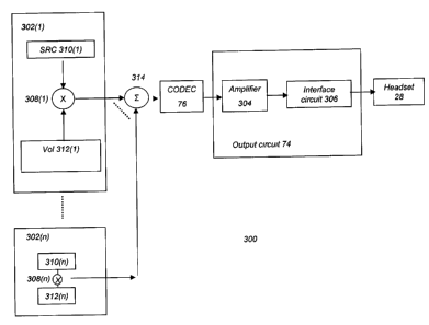
[0071] Referring to Fig. 3, circuit 300 provides two stages of attenuation
control for
CODEC 76. For the first stage, digital control module 302 is provided inside
CODEC 76
and provides data manipulation of the digital output signal. For the second
stage, output
circuit 74 controls attenuation of an analog signal generated from CODEC 76.
The first
and second stages are discussed in turn.
[0072] For the first stage, digital control module 302 has a source input
signal (SRC
310) and a corresponding output volume control signal (VOL 312). The resultant
signal
is combined digitally in summing module 308. The volume control may act to
attenuate
or to amplify the digital signal. The source signal may (or may not) be
attenuated or
amplified (as its digital representation) before being provided to summing
module 308.
There may be multiple modules 302(n) provided where each module 302(n) has a
McCarthy Tetrault LLP DOCS #10743690 v. 2
CA 02754575 2011-09-30
-16-
separate input signal SRC 310(n), volume control signal VOL 312(n) and summing
module 308(n). Signals from all modules 302 are provided to summing module 314
which sums all signals (digitally) and then provides the resultant net digital
value to
CODEC 76. For example for a headphone circuit, a source input signal may be a
music
file and the volume control may be a headphone output. Multiple input sources
may be
paired with corresponding multiple output control signals. Multiple sources
may be
involved where a telephone call output signal is combined with a music file.
The digital
control module may be implemented in processed embedded in output adjustment
module 48G.
[0073] For the second stage, one embodiment provides the second stage in
output
circuit 74 as an operational amplifier ("op amp") 304 and interface circuit
306. Op amp
304, e.g. device MAX97200 (trade-mark) from Maxim Semiconductor, provides an
amplification circuit for audio signals destined for the output device (e.g.
headset 28)
connected to output circuit 74.
[0074] Output circuit 74 may be implemented as a silicon circuit using
polysilicon or
other on-chip resistors to define the resistor values and using NMOS/PMOS
switches to
define which resistors are used. Other circuits using discrete components may
also be
implemented. Interface circuit 306 provides the final physical interface for
output circuit
74 to headset 28. Circuit 306 may include the physical jack to receive the
input plug of
headset 28. A signal may be applied to headset 28 when headset 28 is connected
to
interface circuit 306 via terminal 32 (Fig. 2).
[0075] In one embodiment, output circuit 74 provides isolation and attenuation
of
output signals to headset 28. In one embodiment, op-amp 304 may provide a
dynamic
range of approximately 108 dB. An embodiment allows control of the output
signal from
op amp 304. One output control element is provided following op amp 304. Fig.
4A
shows the output of op amp 304 is connected to a resistive attenuator network,
as
provided in circuit 306. One configuration for circuit 306 provides
approximately
between 0 and 60 dB output attenuation to the signal and approximately between
0 and
20 dB of attenuation of the input signal before applying it to amplifier 304.
More or less
attenuation may be provided in other embodiments. In low output signal
conditions, the
noise floor associated with circuit 74 is decreased as analog circuit Rs and
Rp
attenuates both the signal and the noise. In yet another embodiment,
operational
amplifier 304 provides attenuation of the output signal instead of an external
resistive
McCarthy T6trault LLP DOCS #10743690 v. 2
CA 02754575 2011-09-30
-17-
divider. Such an implementation provides a balance of improved power
efficiency and
against noise level performance.
[0076] One or more additional (analog) attenuation stage(s) may be added in
other
embodiments either before or after op amp 304. As part and / or adjunct to
interface
circuit 306, a resistive network may be implemented to provide attenuation of
signals for
circuit 74. The network may be implemented as a resistor or a set of resistors
provided
in series and / or parallel. As described herein, elements are "in series" if
substantially
the same current flows through them. Elements may be deemed to be in series
even if
the current flowing through them is not exactly the same, such as when a node
between
the first element and the second element, enables a negligible amount of
current to flow
through a third element. The first and second elements would be deemed to be
"in
series: because the current flowing through them would be substantially the
same.
Similarly, elements are "in parallel" if they experience substantially the
same voltage
between two nodes. Once again, the voltages need not be exact, and the two
elements
in parallel need not necessarily be coupled to exactly the same nodes. For
purposes of
simplicity of description, elements in series may be depicted as being
strictly in series,
and elements in parallel may be depicted as being strictly in parallel.
Further, as is well
known, a single resistor can be made up of multiple resistor elements, but for
simplicity,
a resistor will be assumed to be and depicted as a single resistor. A
selection of the
values for the resistors and the type of circuit will determine the
attenuation provided by
the resistors. The resistive network may be selectively coupled to the module
when the
output has been decreased by between approximately 10 and 20 dB by regulating
the
input level to the amplifier. It will be appreciated that at this output power
level, namely
between approximately 10 and 20 dB below a full scale output for headset 28,
power lost
in the load resistors in the resistive network will be relatively small
compared to the
power level of the full circuit. As such, for the headset the embodiment
provides an
output signal that has a noise floor that varies with the output level of the
amplifier.
[0077] As such, while power efficiency for the circuit will be lower for these
relatively
low volume settings, the total power loss is relatively small. A typical
attenuation for low
sensitivity headsets is between about 0 and 30 dB; for medium sensitivity
headsets a
typical attenuation is between about 10 and 45 dB; and for highly sensitive
headsets, a
typical attenuation is between about 25 and 60 dB.
McCarthy T6trault LLP DOCS #10743690 v. 2
CA 02754575 2011-09-30
-18-
[0078] In another embodiment, output circuit 74 provides a load-independent
buffer
through a resistive divider network, which may provide constant gain steps
regardless of
load impedance values. This type of set up may be suitable for low noise or
general
amplification applications.
[0079] Further detail is now provided on the first stage of signal control
provided in
Fig. 3. Referring to Fig. 4A, process 400 illustrates an exemplary process
used to
provide improved headroom performance for controlling an output. Briefly, an
input
signal's value is boosted before being provided to a DAC inside CODEC 76. In
this
embodiment, the input signals before the DAC inside CODEC 76 are in the
digital
domain. As such, the digital signals are boosted before the DAC inside CODEC
76 and
then they are allowed to be attenuated by downstream modules. As previously
noted
signals from the DAC inside CODEC 76 can be attenuated using an analog volume
control. An embodiment maintains a volume level inside CODEC 76 which has
suitable
signal-to-noise ratio and distortion level for the output signal. As with many
analog
circuits, there is a noise floor associated with it. By boosting the original
digital input
signal, the relative gain of the input signal over the noise floor has been
increased. The
analog/digital signal control and attenuation may be provided in a circuit
which utilizes a
combination of one or more hardware and / or software elements.
[0080] Process 400 is suitable for adjusting the digital output level of one
output
source (SCR 1) having one volume control (VOL 1), per Fig. 3. In processing
the digital
signal of the input signal, the following processes are performed. At block
402, process
400 starts. At block 404, a determination is made of a maximum digital input
level for
the DAC inside CODEC 76 for optimal operation of CODEC 76. The maximum input
level is typically specified as 0 dBFS (dB full scale). For optimum operation,
one
embodiment is between approximately 1 and 2 dB below 0 dBFS, namely at
approximately -1 to -2 dBFS. In another implementation, an optimum volume
setting
may be between approximately 0.5 and 6 dB below the maximum allowed value. An
optimum value may be selected for a given DAC depending on its performance
characteristics. The optimal operation may consider one or more of the best
signal to
noise and distortion (SINAD) level, the best signal to noise ration (SNR), the
best
distortion performance, or other parameters. (For the sake of brevity of for
this
disclosure, operating points described herein as the "maximum", "best" or
"optimum" are
understood to include the best, maximum and / or optimum determined operating
point
McCarthy Tetrault LLP DOCS #10743690 v. 2
CA 02754575 2011-09-30
-19-
as well as operating points that pass a certain threshold, unless otherwise
noted.
Similarly, "minimum" and "zero" operating points may be comparably determined
with
additional points passing a minimum or zero value threshold.) Next, at block
406, the
digital gain for the input signal is set to be at the optimum input level for
the DAC inside
CODEC 76. This ensures that the best possible operating point of CODEC 76 is
being
used and that the optimum operating point of CODEC 76 is not exceeded. As an
adjustment in block 406, instead of using the absolute maximum input level,
process 400
will typically adjust the digital gain to provide some headroom between the
maximum
input signal and the maximum range of CODEC 76. This reduction assists in
avoiding
clipping of the output signal and operating the DAC at a suitable performance
point,
which may be the best possible performance point or a level that surpasses a
provided
threshold. The reduction may be in absolute terms (e.g. in dB) or in relative
terms
compared to the output signal (e.g. a percentage of the output signal) or some
combination of both. With the maximum gain level set for the input signals,
downstream
adjustments can be made to the output level of the circuit. As the input
signal has been
boosted, generally, an embodiment provides an attenuation of the signal to
provide
output control at process 408.
[0081] The process of adjusting the (digital) output level for input signals
can be
done at any time. Adjustments may be made when a determination is made that
different output levels are being processed. For example, if it is determined
that the
maximum output level for a signal will not exceed a certain level, then
process 400 can
be performed to determine a suitable gain for that output level. However, if
later it is
determined that the output level for that signal has changed (either upwards
or
downwards), then a different appropriate gain may be determined.
[0082] As a modification to general features of process 400, Fig. 4B, shows
process
400(2), which illustrates an exemplary process used to provide improved
headroom
performance for controlling multiple outputs (e.g. output from a telephone
call with output
of a music file with output of audible enunciators, etc.). Briefly, for all of
the output
signals being combined, the resultant output signal is still boosted to use a
suitable
possible operating point for the input side of CODEC 76 (which may be the best
determined operating point or an operating point that passes a certain
threshold) and to
reduce influence of EMI outside CODEC. However, relative output levels among
sources from the original signals may need to be respected. The relative
levels may be
McCarthy T6trault LLP DOCS #10743690 v. 2
CA 02754575 2011-09-30
-20-
maintained as an absolute value (e.g. in dBs) or as a relative value (e.g.
percentage of
one output level to another output level). At block 402(2), process 400(2)
starts. At
block 404(2), a determination is made for the maximum digital input level for
optimal
CODEC 76 operation, which may relate to the "best" SINAD, SNR, distortion
level, etc.
At block 404b(2), a determination is made for the maximum output based on the
summation of all input streams. Next, at block 406(2) an adjustment is made to
these
streams downward so that the optimal maximum level will never be exceeded. As
such,
the digital gain for the summed output signals is set to be at the optimum
input level for
CODEC 76. Again, as an adjustment in block 406(2), instead of using the
optimum input
level, process 400(2) may downwardly adjust the digital gain to provide some
headroom
between the maximum input signal and the optimum range of CODEC 76 to avoid
clipping when multiple digital sources are added. This reduction assists in
reducing
distortion of the output signal. The reduction may be in absolute terms (e.g.
in dB) or in
relative terms compared to the output signal (e.g. a percentage of the output
signal) or
some combination of both. Typically, the source with the largest volume
setting will be
set to a level near the optimum operating point, adjusted for the additional
amplitude
from the other sources and afterwards the other sources will be adjusted with
respect to
this source. With the optimum gain level set for the input signals, downstream
adjustments can be made to the output level of the circuit to compensate for
the output
level from the DAC at process 408(2). This will happen either in the headphone
output
amplifier or after this system component.
[0083] In processing two exemplary streams, process 400(2) would perform the
following calculations in process 406(2):
1) Calculate the maximum possible amplitude of both streams (stream 1 and
stream 2)
when added together.
2) If (stream 1 > stream 2), then set signal 1 to an optimum value for the
CODEC, while
correcting this to a smaller value to avoid distortion due to source 2. Stream
2 will be
corrected to have the same difference to stream 1 as before the correction. A
check can
be made to ensure absolute value of both streams is correct.
3) If (stream 2 > stream 1) then set signal 2 to an optimum value for the
CODEC, while
correcting this to a smaller value to avoid distortion due to source 1. Stream
1 will be
corrected to have the same difference to stream 2 as before the correction. A
check can
be made to ensure absolute value of both streams is correct.
McCarthy Tr trault LLP DOCS #10743690 v. 2
CA 02754575 2011-09-30
-21-
4) A correction may be provided for the lower limit of the analog gain as
follows. When
the desired output attenuation is higher than possible by the amplifier's or
output
attenuator, the stream can be adjusted digitally to give a lower output level.
5) A final check can be made for against the maximum gain for the output
amplifier. If it
exceeds the maximum output level, then the output level is set to the maximum
level.
These processes can be implemented in output adjustment application 48G.
[0084] With details provided on the first (digital) process stage of Fig. 3,
further detail
is provided the second (analog) stage, as shown in exemplary circuit 74.
Referring to
Fig. 5A, (AC) output voltages from a source with finite output impedance
generally vary
with different loads attached. An embodiment provides a circuit 500 for
reducing noise
level of an output signal from audio amplifier 304. Audio amplifier 304 may be
a non-
inverting amplifier, an inverting amplifier and may or may not have unity
gain. The gain
and/or attenuation of the input signal will typically be programmed by opening
or closing
switches that determines the gain/attenuation of this system component by
selecting
different resistors in the feedback path. By using an operational amplifier
with wide
attenuation range, a system with high efficiency and low noise may be
obtained. The
output of amplifier 304 is provided to interface circuit 306 (Fig. 3)
comprising resistors
502 and 504. Amplifier 304 is coupled to resistor 502 in series. Resistor 502
is coupled
to resistor 504, which is coupled to ground. Resistors 502 and 504 are noted
as
resistances Rs and Rp, respectively. Terminal 32 (Fig. 2) is connected in
parallel to
resistor 504. When a load (e.g. headset 28) is attached to the terminal 32,
the circuit is
complete and headset 28 (which may be considered to be a resistive load for
circuit 500)
is coupled in parallel with resistor 504. In other embodiments, one or more
resistors
may be provided where resistor 502 is located and one or more resistors may be
provided where resistor 504 is located. Also, headset 28 may be connected with
additional passive and / or reactive elements. Additional passive and / or
reactive
elements may be provided along any path in circuit 500. In an embodiment,
circuit 500
provides a constant and but finite, output impedance as a reference. The
finite
impedance provides constant gain steps for different attached loads. Analog
attenuation
may typically provide at least approximately 10 dB or more of attenuation, in
order to
gain the benefits of improved EMI reduction and lower noise when using
separate
CODEC and interface blocks, though other choices may be made depending on a
preference for either noise requirements or reduced power consumption
characteristics.
McCarthy Tetrault LLP DOCS #10743690 v. 2
CA 02754575 2011-09-30
-22-
[0085] Fig. 5B illustrates another embodiment showing circuit 500(2), where an
input
attenuator is provided to supplement the interface circuit 306. For the input
attenuator,
amplifier 304 is coupled to a programmable voltage divider 506 in series,
which is
coupled to ground. The voltage divider may be implemented as a variable
resistor with
an output tap that can be aligned at different resistance points. As such
divider 506
provides a variable resistance. An output tap from divider 506 is provided to
amplifier
304. Divider 506 may be electronically or manually controlled to change its
voltage
divider value. As such, divider 506 changes the amount of current and voltage
provided
to amplifier 304. Divider 506 is an input attenuator for circuit 500(2) and
serves to
provide a mechanism for attenuating the first portion of an output signal
(i.e. the first
coarse adjustment for the output signal). For example if a signal has a range
of
approximately 0 to 100 dB, divider may be used to control attenuation for a
first range
from the current output level for the device.
[0086] The output of amplifier 304 is provided to interface circuit 306 (Fig.
3)
comprising resistors 502(2) and 504(2), as before. Amplifier 304 is coupled to
resistor
502(2) in series. Resistor 502(2) is coupled to resistor 504(2), which is
coupled to
ground. Resistors 502(2) and 504(2) are noted as resistances Rs and Rp,
respectively.
Terminal 32 (Fig. 2) is connected in parallel to resistor 504(2). When a load
(e.g.
headset 28) is attached to terminal 32, the circuit is complete and headset 28
is coupled
in parallel with resistor 504(2). Divider 506 and resistors 502(2) and 504(2)
may each be
a semiconductor based programmable device (such as a resistor, including a
polysilicon
or metal oxide (MOS) resistor). In this configuration an application (such as
OAA 48G)
may provide instructions and access data to set the resistance values of
divider 506 and
resistors 502(2) and 504(2). In other embodiments, one or more resistors may
be
provided where divider 506 or resistor 502(2) is located and one or more
resistors may
be provided where resistor 504(2) is located. Also, headset 28 may be
connected with
additional passive and / or reactive elements when bridging resistor 504(2).
Additional
passive and / or reactive elements may be provided along any path in circuit
500(2).
[0087] For Fig. 5B, since divider 506 is located before op amp 304, when the
signal
is attenuated by divider 506, the resulting smaller output is closer to the
noise floor of op
amp 304. However, since divider 506 is used primarily for the first portion of
signal
attenuation (e.g. for approximately the first 0-18 dB of attenuation), the
noise floor
cannot generally be noticed as the signal is being attenuated by divider 506.
McCarthy Tetrault LLP DOCS #10743690 v. 2
CA 02754575 2011-09-30
-23-
[0088] Now, further detail is provided on specific implementations of circuits
500 and
500(2), in particular, detail is provided on algorithms for establishing
exemplary values
for Rs and Rp. Through calculations shown below, Table A shows values for Rs
and Rp
that may be used for an embodiment for circuits 500 and 500(2). The noted
attenuation
value is the amount of attenuation (in dB). For a given desired attenuation
level in the
volume (e.g. approximately -2 dB, -4 dB, etc.) the paired values of Rs and Rp
in the
corresponding columns may be used. For example, when a -2 dB attenuation level
is
desired as the output to headset 28, then for circuit 500, Rs should be set at
approximately 10.0714 ohms and Rp should be set at approximately 38.8969 ohms.
The values can be set of approximate resistance values from the functions,
e.g.
resistance values rounded to the first decimal point (e.g. to 38.9 ohms) or
less precise
values (i.e. first digit, to 39 ohms, or other tolerances). The different
values of Rs and
Rp may be provided via a silicon-based programmable resistor, where the values
may
be selected inside the related silicon chip by (electronic) switches
implemented using
NMOS/PMOS transistors.
Table A
Attenuation [dB] Ideal values
(compared to
reference level) Rs [0] Rp [0]
0.00 8.00 00
-2.00 10.0714 38.8969
-4.00 12.6791 21.6777
-6.00 15.9621 16.0381
-8.00 20.0951 13.2914
-10.00 25.2982 11.6998
-12.00 31.8486 10.6836
[0089] As shown, for an attenuation of between -2.00 dB and -12.00 dB, Rs has
a
value of between approximately 10 0 and 32 f2 and Rp has a value of between
approximately 390 and 100.
[0090] Rs, as placed in series prior to headset 28, affects the current that
is provided
to headset 28. A larger value of Rs limits more current to headset 28. Rp, as
placed in
parallel to headset 28, reduces the load impedance sensitivity of headset 28
for circuits
500 / 500(2). A smaller value of Rp may effectively makes the load impedance
McCarthy T6trault LLP DOGS #10743690 v. 2
CA 02754575 2011-09-30
-24-
sensitivity to be close to, or effectively at, zero. An embodiment also
provides an inverse
relationship, specifically a hyperbolic relationship, in the value of Rs to
Rp. In particular,
in one embodiment the values of Rs and Rp may be calculated from the following
functions:
Rs = Rx / a Equation 1
Rp = Rx / (1-a) Equation 2
where Rx is the series resistance used with no attenuation (providing a
reference value)
and a is the desired attenuation in absolute value, i.e. attenuation = -20
log(a). For
example, an attenuation of 2 dB results in a having a value of 0.7943. In
Table A shown,
Rx = 8 Q. It can be seen that Rs and Rp are related to each other in an
inversely
proportional manner. Generally, for the purposes of an example and not
limitation, the
inverse proportionality relationship between Rs and Rp is that as one value
(e.g. Rs)
increases, the other value (e.g. Rp) decreases. Here a is a scaling factor for
the
relationship. Other scaling factors and offsets can also be provided. In other
embodiments, an inverse proportional relationship may include step-wise
function(s)
where changes in one value impart a change on the other only after a certain
change
threshold is reached.
[0091] For an embodiment and Table A, the individual attenuation steps shown
therein may be set and calculated for a given application. If many attenuation
steps are
required, then, an embodiment may use many resistors and many switches. An
embodiment may use a few (e.g. 1, 2 or 3) steps, e.g. one step or a few large
steps such
as 0 and -12 or 0 and -20 dB, and implement additional attenuation stages
elsewhere.
[0092] It is noted that the minimum value of Rs is not zero. As such, there
may be a
small signal attenuation associated with this embodiment. A finite (and small)
value for
Rs has been provided, since it is necessary in order that the first step (e.g.
about -2 dB)
does not differ too much between the smallest and largest possible loads. It
is
preferable that the minimum value of Rs should not be chosen to be too small,
since this
may result in very heavy load for a large attenuation. It is also preferable
that the value
of Rs should not be chosen to be too large, since the default output
(reference output,
zero dB), may mean the signal would be excessively attenuated. From
experimentation,
it was determined that a starting point of Rx = 8 0 provides a good compromise
between
providing a minimum load and maximum attenuation for headsets.
McCarthy Tetrault LLP DOCS #10743690 v. 2
CA 02754575 2011-09-30
-25-
[0093] In an embodiment, the values Rs and Rp may be determined using the
above
Equation 1 and Equation 2 by selecting a value for a, instead of a desired
attenuation.
For example, if a is chosen to be 0.625 and Rx is 8 0, then the Rs value would
be 12.8
0 and Rp would be 21.3f), and the corresponding attenuation would be the
negative
value of -20 * log(a) which is -4.08 dB.
[0094] In yet another embodiment, the load impedance sensitivity may be
removed
where the relationship between values Rs and Rp is governed by the following
function:
Rp = Rs * a / (1-a) Equation 3
where a is the desired attenuation value. Rs is selected as a compromise
between a
small finite value to give small difference between minimum and maximum
connected
load and a large value to limit power consumption. As can be seen with
Equation 3, for
a=1 (representation an implementation with no attenuation), the Rp value will
be infinite,
representing an arbitrarily large value, i.e. an open circuit.
[0095] The resistive divider networks of interface circuits 306 shown in
circuits 500
and 500(2) may be implemented using programmable resistors (e.g. using a
polysilicon
layer or other resistor implemented on a silicon chip). The resistive control
may be
changed at low volume output levels (e.g. less than approximately 5 mW in
output
wattage) and then changed again at higher volume levels. For example, a change
to the
values may be implemented by first activating an input attenuator (e.g.
divider 506, Fig.
5B, or another resistive element located before amplifier 304) when the noise
floor is not
within a certain value. This may be when the output is at a relatively high
level. When
the output of the amplifier is nearing a deemed noise floor and crosses a
threshold, then
an embodiment may utilize the interface circuit 306 components to provide an
output
attenuator for low-level amplification control. This may be done while keeping
any
current settings for divider 506. Prior to activation, the output attenuator
may be set to a
resistance value that is at or near 0 ohms. In other embodiments, the input
and output
attenuators may be controlled together when operating above or below a given
threshold. Multiple thresholds can be provided where multiple adjustments to
the
controlled elements are provided. When controlling an output signal both the
input and
output attenuators may work together. When controlling a low level signal, the
values for
Rs and Rp for the output attenuator may be dynamically controlled with the
values for
the input attenuator to provide equal-step attenuation of the signals. With
such an
implementation, low power consumption may be achieved.
McCarthy Tetrault LLP DOCS #10743690 v. 2
CA 02754575 2011-09-30
-26-
[0096] The output load resistors or load transistor may use a component having
a
low wattage rating (and physical size) to the small dissipated power. Even
though
precise step-wise volume adjustments are provided with above-described
embodiments,
there may be some difference in transfer function for the absolute
attenuation, which
may be acceptable in practice.
[0097] As noted, each of divider 506 and interface circuit 306 may attenuate
the
output signal of op amp 304. An embodiment allows divider 506 and circuit 306
to
collectively attenuate signals. To provide same, each component is used at
different
stages of attenuation of the output signal.
[0098] To use both components, first, a range of attenuation for output
signals for op
amp 304 is determined. For the sake of illustration, a range of approximately
0 to 30 dB
is used to describe features of this embodiment. For a first range of
attenuation, divider
506 is used. Since divider 506 is located before op amp 304 values for
components of
the divider circuit would be smaller for a comparable divider circuit located
at the output
of op amp 304. An exemplary first range is approximately 0 to 20 dB of
attenuation is
provided by divider 506. When attenuation is being initiated, divider 306 is
programmed
with its correct values to cover the first range of attenuation. For a second
range of
attenuation, as the noise floor of op amp 304 approaches the signal level
being
processed by op amp 304, interface circuit 306 is used to implement further
attenuations
of signal and noise. The values for Rs and Rp in circuit 306 are determined
based on a
step-wise output value selected for circuit 300 (Fig. 3), as noted above. At
this point,
depending on the step-wise value selected, values for Rs and Rp may be
programmed
into their components. As the attenuation scale for the second range is
reached, a third
attenuation range may be provided. For the third range, divider 506 may be set
to
provide even more attenuation than the first range and then circuit 306 may be
re-
calibrated with new values for Rs and Rp to further process attenuating
signals. More or
less stages can be provided in other embodiments. Also, for a given stage,
both divider
506 and circuit 306 may dynamically change their configurations to
collectively provide a
net attenuated signal using both stages for op amp 304. In yet another
configuration
digital attenuation is used when the analog attenuation has resulted in a
sufficiently low
noise floor, e.g. equivalent to the ambient acoustic noise when taking the
transducer
sensitivity into account.
McCarthy T6trault LLP DOCS #10743690 v. 2
CA 02754575 2011-09-30
-27-
[0099] It will be appreciated that for some mathematical values calculated for
Rs and
Rp, actual resistive values available (whether as discrete components or
resistive values
provided in a programmable resistor) for production modules, may not be
identical to the
calculated values. As such, when implementing a circuit for an embodiment,
there may
be differences between the desired and real values for the resistors selected
for the
programmable resistor. In the design stage, efforts can be made to track the
available
values to the calculated values, which may result in providing an
implementation that
may accurately track the calculated values. With the circuit, an embodiment
provides a
constant dynamic range over a wide range of output signals. This is due to the
fact that
both the output signal and the noise are attenuated (thus keeping the signal-
to-noise
ratio constant). This has an advantage over other systems that attenuate the
output
signal through other means (e.g. digitally at the microprocessor alone), since
in those
systems, the attenuation will only attenuate the signal, but will not
attenuate the noise
level, which results in a decrease of the signal-to-noise ratio with larger
attenuation. For
an embodiment, the effects of thermal noise in the resistors are deemed to be
negligent.
Other embodiments may take into consideration adjustments for such noise or
other
sources of noise (e.g. through filtering circuits and capacitors).
[00100] It will be appreciated that other filter circuits and other values for
resistors
shown in Figs. 5A and 5B may be provided in other embodiments. It will also be
appreciated that other isolation/attenuation systems may be provided for other
input/output stages for a device.
[00101] Referring to Fig. 5C, in another embodiment, a divider arrangement
using two
complex impedances is provided. The output of amplifier 302 is provided to
interface
circuit 306 comprising impedance 502(3) and 504(2). Amplifier 304 is coupled
to
impedance 502(3) in series. Impedance 502(3) is coupled to impedance 504(3),
which
is coupled to ground. Impedances 502(3) and 504(3) are noted as impedances Zs
and
Zp, respectively. Terminal 32 (Fig. 2) is connected in parallel to impedance
504(3).
When an impedance load (e.g. headset 28) is attached to terminal 32, the
circuit is
complete and headset 28 is coupled in parallel with impedance 504(3). In other
embodiments, one or more impedances may be provided where impedance 502(3) is
located and one or more impedances may be provided where impedance 504(3) is
located. Also, impedance load 28(3) may be connected with additional passive
and / or
McCarthy Tetrault LLP DOCS #10743690 v. 2
CA 02754575 2011-09-30
-28-
reactive elements when bridging impedance 504(3). Additional passive and / or
reactive
elements may be provided along any path in circuit 500(3).
[00102] In an embodiment, circuit 500(3) provides a constant and finite output
impedance as a reference. The finite impedance provides constant gain steps
for
different attached loads, where impedances are determined from the following
functions:
Zs = Zx / a Equation 4
Zp = Zx / (1-a) Equation 5
where Zx is a reference impedance.
[00103] Now further details are provided on processes for identifying and
selecting
parameters for circuits of an embodiment.
[00104] Fig. 6 illustrates an exemplary process 600 for selecting the
resistors in a
resistive divider network for maintaining a constant dynamic range of an
output signal
from an amplifier in accordance with an embodiment of the application, which
summarizes features previously discussed. At block 602, a desired attenuation
in dB is
chosen. At block 604, the value of a is calculated using the chosen
attenuation value in
accordance with the above formulae. At block 606, the value of Rx is selected.
At block
608, the resistance values Rs and Rp are calculated in accordance with
Equation 1 and
Equation 2. At block 610, a first resistor with a resistance of Rs and a
second resistor
with a resistance of Rp are selected. In practice, resistance values may
follow distinct
steps so resistors having resistances approximate to the Rs and Rp may be used
for
implementing an embodiment of the application.
[00105] Alternatively, the resistors in the resistive divider network may be
selected by
first choosing a value for a and, in such a case, only processes in blocks
606, 608 and
610 may be executed.
[00106] Fig. 7 shows experimental data of deviations from ideal response based
on
fifty (50) simulations and an individual variation of 2% (standard deviation).
The
deviations may in this case be up to approximately 0.6 dB, which may be
acceptable
since the attenuator is intended to be used for audio purposes. The load
values were 16
), 32 U, 72 0 and 10 kit. It can be seen, that the majority of the variation
is within 0.2
dB, although some shown values reach +0.6 dB. Note that the volume setting "1"
McCarthy T6trault LLP DOCS #10743690 v. 2
CA 02754575 2011-09-30
-29-
corresponds to a reference attenuation and therefore there is no deviation for
any of the
resistor values.
[00107] It will be appreciated that the above described principles may be used
for
maintaining a constant dynamic range over a large attenuation range of an
input signal
from external devices connected to device 10, which may be achieved by
reversing the
resistance values Rs and Rp of the resistor components of the resistive
divider network.
[00108] As used herein, the wording "and / or" is intended to represent an
inclusive-
or. That is, "X and / or Y" is intended to mean X or Y or both.
[00109] Exemplary advantages or benefits that may be realized from aspects of
this
disclosure include improved audio quality and flexibility of control with
circuits by having
first and second stages as described, with each stage being independently
designed,
while still acknowledging one stage's effect on the other stage. Flexibility
is further
provided by digital control allowing real time adjustments to be made to
operating
parameters of both the first and second stages.
[00110] In this disclosure, where a threshold or measured value is provided as
an
approximate value (for example, when the threshold is qualified with the word
"about"), a
range of values will be understood to be valid for that value. For example,
for a
threshold stated as an approximate value, a range of about 25% larger and 25%
smaller
than the stated value may be used. Thresholds, values, measurements and
dimensions
of features are illustrative of embodiments and are not limiting unless noted.
Further, as
an example, a "sufficient" match with a given threshold may be a value that is
within the
provided threshold, having regard to the approximate value applicable to the
threshold
and the understood range of values (over and under) that may be applied for
that
threshold.
[00111] It will be appreciated that the embodiments relating to circuits,
algorithms,
devices and systems may be implemented in a combination of electronic
circuits,
hardware, firmware and software. The circuits may be implemented in whole or
in part
through a combination of analog and / or digital components. In a circuit, an
element
may be connected to another element either directly or through another
circuit. When a
first element is identified as being connected to another element, that first
element itself
may be considered to be a "circuit". All components having stated
McCarthy Tetrault LLP DOCS #10743690 v. 2
CA 02754575 2011-09-30
-30-
resistances/inductances may be implemented in discrete (analog) components, in
programmable components or a combination of both. The firmware and software
may
be implemented as a series of processes, applications and/or modules that
provide the
functionalities described herein. The algorithms and processes described
herein may be
executed in different order(s). Interrupt routines may be used. Data may be
stored in
volatile and non-volatile devices described herein and may be updated by the
hardware,
firmware and/or software.
[00112] It will further be appreciated that all processes, algorithms, steps
etc. as
described herein may be conducted in a single entity. For example the
calculations for
the first and / or second stages may be provided in the device itself. Such
calculations
may be conducted by one or more modules in the device. The disclosure as such
provides a method of operating a device and / or a method for a function,
operating on
the device. Alternatively, such calculations may be conducted in an off-site
location (e.g.
a design laboratory) and the resulting circuits and calculations can be
provided to the
device. The disclosure as such also provides a method of manufacturing, making
and /
or assembling the device.
[00113] The present disclosure is defined by the claims appended hereto, with
the
foregoing description being merely illustrative of embodiments of the
disclosure. Those
of ordinary skill may envisage certain modifications to the foregoing
embodiments which,
although not explicitly discussed herein, do not depart from the scope of the
disclosure,
as defined by the appended claims.
McCarthy Tetrault LLP DOCS #10743690 v. 2