Note: Descriptions are shown in the official language in which they were submitted.
CA 02755089 2016-09-27
UNIVERSAL RFID TAGS AND MANUFACTURING METHODS
BACKGROUND OF THE INVENTION
1. Field of the Invention
The present invention relates generally to radio frequency identification
(RFID) tags, and
more specifically to RFID tags suitable for use in near and far range
applications.
2. Discussion of the Related Art
A radio frequency identification (RFID) tag is an object that can be applied
to or
incorporated into a product, animal, or person for the purpose of
identification and tracking using
radio waves. Some tags can be read from several meters away and beyond the
line of sight of the
reader. Most RFID tags contain at least two parts. One is an integrated
circuit for storing and
processing information, modulating and demodulating a radio-frequency (RF)
signal, and other
specialized functions. The second is an antenna for receiving and
backscattering the signal.
There are generally two types of RFID tags: active RFID tags, which contain a
battery, and
passive RFID tags, which have no battery. Today, RFID is used in enterprise
supply chain
management to improve the efficiency of inventory tracking and management.
Wal-Mart and the U.S. Department of Defense have published requirements that
their
vendors place RFID tags on all shipments to improve supply chain management.
Typically,
vendors use RFID printer/encoders to label cases and pallets that require
electronic product code
(EPC) tags. These smart labels are produced by embedding RFID inlays inside
the label
material, and then printing bar code and other
1
CA 02755089 2011-09-09
WO 2010/104991
PCT/US2010/026882
visible information on the surface of the label.
However, vendors face significant difficulties implementing RFID systems.
For example, the successful read rates currently run only 80%, due to radio
wave
attenuation caused by the products and packaging. That is, the RF
characteristics and
performance of a RFID UHF passive tag vary depending on the dielectric
properties
of the object it is placed on. Tag inlay manufacturers attempt designing tags
that are
the least effected by the object's dielectric. The dielectric of the item the
tag is
attached to changes the resonate frequency of the inlay's antenna. In order
for the RF
signal to get to the integrated circuit there has to be an impedance matching
between
the antenna and the chip. The more the antenna is detuned, the greater the
impedance
is mismatched. The tag's performance degrades as the impedance mismatch
increases
until the tag stops working.
Inlay manufacturers have had only moderate success at designing "universal
tags" that will reliably function for all uses. The alternative is to design
specific tags
for specific types of product. As a further challenge, vendors will need to
design tags
that will meet tag certification which requires a particular tag be used for
proper
performance so that the tag can be read under many varying conditions through
out
the supply chain. This will lead to even more product specific tag designs.
Additionally, the manufacturers of consumer products will have to keep
inventory of all the different tags that are required to sell their products.
The right tag
for a particular stock keeping unit (SKU) will have to be added to the Bill of
Materials
as a component and be managed through Materials Requirements Planning (MRP).
This adds one more link that can potentially stop the productions line for
that SKU.
There will be great pressure to substitute a different non-certified tag in
order to keep
the production line moving which will cause inventory inaccuracies down the
supply
chain. The burden to the supply chain both in cost and complexity creates a
head
wind that suppliers to retailers that require RFID tagging have to overcome.
-2-
CA 02755089 2011-09-09
WO 2010/104991
PCT/US2010/026882
SUMMARY OF THE INVENTION
Several embodiments of the invention provide radio frequency identification
(RFID) devices, and methods of manufacturing the same. In one embodiment, the
invention can be characterized as a radio frequency identification (RFID)
device
comprising: a near field only RFID tag that does not function as a far field
RFID tag
and is pre-manufactured; and a conductive element independent from the near
field
only RFID tag and adapted to function as a far field antenna. The near field
only
RFID tag is coupled to a first portion of an item; and the conductive element
is
coupled to a second portion of the item, the first portion and the second
portion
located such that the near field only RFID tag is coupled in proximity to the
conductive element such that the RFID device functions in both a near field
and a far
field.
In another embodiment, the invention can be characterized as a radio
frequency identification (RFID) device comprising: a near field only RFID tag,
wherein the near field only RFID tag does not function as a far field RFID
tag; a
conductive element independent from the near field only RFID tag and adapted
to
function as a far field antenna; and a coupling structure adapted to locate
the
conductive element in a proximity relationship with the near field only RFID
tag to
couple the conductive element to the near field only RFID tag such that the
RFID
device functions in both a near field and a far field. The coupling structure
is adapted
to allow the proximity relationship of the conductive element and the near
field only
RFID tag to be later removed to decouple the conductive element from the near
field
only RFID tag such that the RFID device no longer functions in the far field.
In a further embodiment, the invention may be characterized as a method of
making a radio frequency identification (RFID) device comprising: coupling a
near
field only RFID tag to a first portion of an item, wherein the near field only
RFID tag
does not function as a far field RFID tag and is pre-manufactured; coupling a
conductive element to a second portion of the item, wherein the conductive
element is
adapted to function as a far field antenna; and wherein the coupling steps
result in that
the near field only RFID tag is located proximate to and coupled in proximity
to the
conductive element such that the RFID device functions in both a near field
and a far
-3-
CA 02755089 2011-09-09
WO 2010/104991
PCT/US2010/026882
field.
In a further embodiment, the invention may be characterized as a method of
making a radio frequency identification (RFID) device comprising: obtaining a
near
field only RFID tag that does not function as a far field RFID tag and is pre-
manufactured; tuning a conductive element to an item to be tagged, the
conductive
element adapted to function as a far field antenna; and coupling the near
field only
RFID tag and the conductive element to the item such that the conductive
element is
coupled in proximity to the near field only RFID tag, wherein the RFID device
will be
adapted to function in both a near field and a far field.
BRIEF DESCRIPTION OF THE DRAWINGS
The above and other aspects, features and advantages of several embodiments
of the present invention will be more apparent from the following more
particular
description thereof, presented in conjunction with the following drawings.
FIG. 1 is a diagram illustrating the basic components of an RFID system
including a passive RFID tag and tag reader as is conventionally known.
FIG. 2A is a diagram of an RFID tag including an integrated circuit chip and
an antenna formed on a substrate as is conventionally known.
FIG. 2B is a diagram of a near field only RFID tag including an integrated
circuit chip formed on a substrate according to one embodiment.
FIG. 2C is a diagram of a near field only RFID tag including an integrated
circuit chip formed on a substrate to allow for capacitive coupling with a far
field
antenna according to another embodiment.
FIG. 3A is a diagram of a decoupled near field only RFID tag and a far field
antenna located in proximity to provide a magnetic coupling therebetween such
that
the near field only RFID tag and the far field antenna function in both the
near field
and the far field in accordance with one embodiment.
FIG. 3B is a diagram that illustrates the removing of the proximity
relationship
between the near field only RFID tag and the far field antenna such that the
RFID
device no longer functions as a far field RFID tag in accordance with one
-4-
CA 02755089 2011-09-09
WO 2010/104991
PCT/US2010/026882
embodiment.
FIG. 3C is a diagram that illustrates the re-location of the near field only
RFID
tag and the far field antenna to be in proximity to each other to provide a
magnetic
coupling therebetween such that the near field only RFID tag and the far field
antenna
again function in both the near field and the far field in accordance with one
embodiment.
FIG. 3D is a diagram of a decoupled near field only RFID tag and a far field
antenna located in proximity to provide a capacitive coupling therebetween
such that
the near field RFID tag and the far field antenna function in both the near
field and the
far field in accordance with one embodiment.
FIG. 3E is a diagram that illustrates the removing of the proximity
relationship
between the near field only RFID tag and the far field antenna such that the
RFID
device no longer functions as a far field RFID tag in accordance with one
embodiment.
FIG. 3F is a diagram that illustrates the re-location of the near field only
RFID
tag and the far field antenna to be in proximity to each other to provide a
capacitive
coupling therebetween such that the near field only RFID tag and the far field
antenna
again function in both the near field and the far field in accordance with one
embodiment.
FIG. 4A is an illustration of a conventional manufacturing process used to
create an RFID tag applied to an item.
FIGS. 4B, 4C and 4D are illustrations of various manufacturing processes
where the manufacturing of a near field only RFID tag and a far field antenna
are
decoupled in accordance with several embodiments.
FIG. 4E is an illustration of a decoupled manufacturing process in accordance
with several embodiments.
FIG. 5 is a cross sectional view of one implementation of a decoupled near
field only RFID tag and far field antenna as affixed to an item in accordance
with one
embodiment.
FIG. 6 is a cross sectional view of another implementation of a decoupled near
-5-
CA 02755089 2011-09-09
WO 2010/104991
PCT/US2010/026882
field only RFID tag and far field antenna as affixed to an item in accordance
with one
embodiment.
FIG. 7 is a cross sectional view of a further implementation of a decoupled
near field only RFID tag and far field antenna as affixed to an item in
accordance with
one embodiment.
FIG. 8 is a cross sectional view of another implementation of a decoupled near
field only RFID tag and far field antenna as affixed to an item in accordance
with one
embodiment.
FIG. 9 is a cross sectional view of another implementation of a decoupled near
field only RFID tag and far field antenna as affixed to an item including an
air gap
maintained between the near field tag and the far field antenna in accordance
with one
embodiment.
FIG. 10 is an illustration of a portion of an item packaging in which a far
field
antenna is formed on a surface of the item packaging in accordance with one
embodiment.
FIGS. 11-13 are illustrations of example items to incorporate RFID tagging
devices wherein the far field antenna design is incorporated into the product
label
design in accordance with several embodiments.
FIG. 14 is a cross sectional view of another implementation of a decoupled
near field only RFID tag and far field antenna as affixed to an item in
accordance with
one embodiment.
FIG. 15 is an illustration of a portion of an item packaging in which a far
field
antenna is formed on a surface of the item packaging in accordance with a
variation of
the embodiment of FIG. 10.
FIG. 16 is one embodiment of the portion of the item packaging of FIG. 15
including a near field only RFID tag capacitively coupled to the far field
antenna.
FIG. 17 is a flowchart of the steps performed in one or more manufacturing
methods in accordance with several embodiments.
Corresponding reference characters indicate corresponding components
throughout the several views of the drawings. Skilled artisans will appreciate
that
-6-
CA 02755089 2011-09-09
WO 2010/104991
PCT/US2010/026882
elements in the figures are illustrated for simplicity and clarity and have
not
necessarily been drawn to scale. For example, the dimensions of some of the
elements in the figures may be exaggerated relative to other elements to help
to
improve understanding of various embodiments of the present invention. Also,
common but well-understood elements that are useful or necessary in a
commercially
feasible embodiment are often not depicted in order to facilitate a less
obstructed view
of these various embodiments of the present invention.
DETAILED DESCRIPTION
The following description is not to be taken in a limiting sense, but is made
merely for the purpose of describing the general principles of exemplary
embodiments. The scope of the invention should be determined with reference to
the
claims.
Reference throughout this specification to "one embodiment," "an
embodiment," or similar language means that a particular feature, structure,
or
characteristic described in connection with the embodiment is included in at
least one
embodiment of the present invention. Thus, appearances of the phrases "in one
embodiment," "in an embodiment," and similar language throughout this
specification
may, but do not necessarily, all refer to the same embodiment.
According to several embodiments, the design of the near field RFID tag
component and the far field antenna of a typical RFID tag is decoupled. For
example,
in one embodiment, the design of the near field RFID tag component is
independent
of the design of the far field antenna that will be used together with the
near field
RFID tag component. In some forms, this will allow a vendor to design or
select the
best or most cost effective near field only RFID tag without regard for the
design of
the far field antenna, and vice versa. Furthermore, when designing RFID tags
according to some embodiments, a vendor can use a single near field only RFID
tag
for all uses, which leads to economies of scale lowering the cost of tagging
items to
the vendor. Additionally, the design of the far field antenna is simplified
when it does
not have to be integrated into the same substrate package as the near field
only RFID
tag. For example, according to some embodiments, a near field only RFID tag
that
-7-
CA 02755089 2011-09-09
WO 2010/104991
PCT/US2010/026882
does not include a far field antenna and does not function as a far field RFID
tag is
mass produced by a tag manufacturer and purchased by the item designer and/or
manufacturer who designs, manufactures, or has manufactured the far field
antenna
which is substantially tuned to the item. In many cases, the result is a cost
effective
and efficient RFID tag that functions as both in the near field tag and the
far field and
is substantially tuned to the item to be tagged.
Referring first to FIG. 1, a diagram is shown of the basic components of an
RFID system 100 including a passive RFID tag 102 and a tag reader 106 as is
conventionally known. The RFID tag 102 is formed on a substrate and includes
an
integrated circuit or chip (not shown) for storing and processing information,
modulating and demodulating a radio-frequency (RF) signal, and other
specialized
functions. The RFID tag 102 also includes a tag antenna 104. In a passive
system,
the reader 106 includes a reader antenna 108 and transmits a modulated radio
frequency (RF) signal 110 to the RFID tag 102. The tag antenna 104 receives
the RF
signal and forms an electric and magnetic field from which the RFID tag 102
draws
power for the integrated circuit. The integrated circuit then causes the RFID
tag 102
to modulate a backscatter RF signal 112 back to the tag reader 106, the RF
signal
containing information encoded in the memory of the RFID tag 102. This is
referred
to as backscattering in that a portion of the energy transmitted by the reader
106 is
reflected by the tag antenna 104 and modulated with data. Both the RFID tag
102 and
the tag reader 106 are transponders. The functionality and operation of the
system
100 of FIG. 1 is well known.
Most RFID tags designed for use in enterprise supply chain management are
designed as both near field and far field RFID tags, i.e., they are designed
to operate
in both the near field and the far field. The near field is the region about
the reader
antenna 108 where the reader antenna 108 and the tag 102 are coupled within
one full
wavelength of the carrier wave; however, in many practical applications, the
near
field is within one half wavelength of the carrier wave. The near field signal
decays
as the cube of the distance from the reader antenna (143). The far field is
that region
about the reader antenna 108 where the reader antenna 108 and the tag 102 are
coupled beyond one full wavelength of the carrier wave. The far field signal
decays
as the square of the distance from the reader antenna (142). In a typical
ultra-high
-8-
CA 02755089 2011-09-09
WO 2010/104991
PCT/US2010/026882
frequency (UHF) RFID system where the carrier frequency is in the range of 860-
960
MHz, the effective near field is the region up to approximately 10-15
centimeters
from the reader antenna 108, whereas the far field is the region from
approximately
15-40 centimeters and beyond the reader antenna 108. In many cases, the reader
106
can read in the near field up to about 15 centimeters away, whereas depending
on the
tag antenna, the reader 106 can read in the far field up to about 20-30 feet
or more
away. These features are also well known in the art.
In a typical enterprise supply chain management application, it is desired
that
the RFID tag 102 be a near field and far field tag to allow it to be read from
the near
field and the far field. The typical RFID tag 102 is an integrated package
that
includes an integrated circuit encoding an identification and a loop to give
it the near
field tag functionality. However, since this loop does not respond to the far
field, the
integrated package also includes a far field antenna or tag antenna that gives
it the far
field tag functionality. The typical far field antenna is a dipole antenna.
The far field
antenna is usually electrically coupled to the near field loop and the
integrated circuit
in most integrated RFID tags, but in some cases, the far field antenna is not
electrically coupled to the near field loop or the integrated circuit and
relies on
inductive or magnetic coupling. The near field loop and the far field antenna
are
commonly printed or etched on the substrate as part of the same
printing/etching
process and then the integrated circuit is carefully placed thereon. The
resulting
integrated device is referred to as an RFID inlay.
There are several problems with this integrated design of the RFID tag 102.
First, it is well known that dielectric properties of the item that the RFID
tag is
attached to affect the performance of the far field antenna. That is, the
dielectric of
the item may change the resonate frequency of the inlay's far field antenna.
In order
for the RF signal to get to the integrated circuit there has to be an
impedance matching
between the far field antenna, the loop and the chip. The more the far field
antenna is
detuned, the greater the impedance is mismatched. The tag's performance
degrades
as the impedance mismatch increases until the tag stops working. Certain
products in
a retail environment are known to possess dielectric qualities that make it
challenging
to design good performing RFID tags. For example, the cleanser Pine-Sol
results in
the detuning of the far field antenna. Knowing this problem, the vendor can
design
-9-
CA 02755089 2011-09-09
WO 2010/104991
PCT/US2010/026882
the RFID tag 102 to tune the far field antenna so that the far field antenna
will match
the impedance with the chip and the loop when applied to the problem item.
Typically, the length of the far field antenna is altered, e.g., shortened, to
tune the
antenna properly to the item it will be attached. However, due to the
integration of
the near field RFID tag and the far field antenna, in changing the far field
antenna to
be tuned to a particular item, the supplier will require a different
integrated RFID tag
for different products. Thus, in some embodiments, the design of the near
field tag
and the far field antenna need to account for each other. Again, this will
cause
suppliers to need to stock several different integrated RFID tags suitable for
various
products.
Referring briefly to FIG. 4A, a conventional manufacturing process is shown
for creating an RFID tag 402 to be applied to an item. The RFID tag 402 is
first
designed as an integration of a near field RFID tag 404 and a far field
antenna 406 as
described above (e.g., the near field loop and far field antenna are printed
or etched on
a substrate and the integrated circuit is positioned thereon). The design of
the near
field RFID tag 404 and the far field antenna 406 must account for each other
and for
the dielectric properties of the item 408 it will eventually be affixed to.
Once the
RFID tag 402 design is complete, the RFID tags are manufactured by or for the
supplier and then applied to the item 408. In some cases, the RFID tag 402 is
located
on the under side of an adhesive sticker or other label and adhered to the
item. In
other cases, the RFID tag 402 integrated into the item or it's packaging
during
manufacturing of the item 408. In these cases, due to the harsh environment of
manufacturing of the item (for example, due to printing, heat, high speed,
etc.), it is
common to damage the RFID tag 402. This makes it more difficult for a supplier
or
vendor to certify that the RFID tag will operate at an acceptable read rate.
Finally,
once the RFID tag 402 is added or affixed to the item 408, the result is a
tagged item
410.
As a solution to one or more of the problems above and/or other problems, in
some embodiments, the manufacturing and design of the near field RFID tag
component is decoupled from or independent of the manufacturing and design of
the
far field antenna. In some embodiments, the goal is not to design a fully
integrated
and packaged RFID tag including both a near field RFID tag and the far field
antenna
-10-
CA 02755089 2011-09-09
WO 2010/104991
PCT/US2010/026882
on the same substrate. In several embodiments, a universal tag can be designed
using
only a simple pre-manufactured near field only RFID tag and a separate and
independently designed conductive element that will function as the far field
antenna.
Since the design of the two components will be separate, in some embodiments,
the
same near field only RFID tag can be used for all items or products to be
tagged. To
account for the varying degree of de-tuning effect caused by certain items or
products,
only the conductive element need be specifically designed. For example, in the
case
of a conductive element in the form of a simple wire, the length of the wire
can be
shortened to match the impedance of the far field antenna to the integrated
circuit.
FIG. 2A illustrates a simple pre-manufactured RFID tag 201 including an
integrated circuit 204 (or chip 204), a loop 202 and a tag antenna 203 (far
field
antenna) formed on a substrate 206 as is conventionally known. In one example,
the
RFID tag 201 is the ImpinjO Paper C1ipTM commercially available from Impinj,
Inc.
The RFID tag 201 functions as both a near field and far field RFID tag, i.e.,
it
functions in and may be read from both the near field and the far field.
FIG. 2B illustrates a near field only RFID tag 200 including the integrated
circuit 204 (or chip 204) and the loop 202 formed on the substrate 206, but
lacking the
tag antenna 203, in accordance with several embodiments. In one embodiment,
the
near field only RFID tag 200 may be formed by removing the tag antenna 203 of
the
device of FIG. 2A. In another embodiment, the near field only RFID tag may be
pre-
manufactured to not include the tag antenna 203. According to several
embodiments,
the near field only RFID tag 200 does not function as a far field RFID tag,
i.e., on its
own, it can not be read in the far field by a tag reader 106. In preferred
embodiments,
the loop 202 is designed, shaped and/or configured to be suitable for use with
a far
field antenna to be electromagnetically and/or electrically coupled thereto.
This is in
contrast to known pre-manufactured near field only RFID tags that are designed
for
use only in the near field. For example, the Impinjt ButtonTM is a near field
only tag
that has a chip with a circular loop and is not designed to be used with a far
field
antenna. Thus, this device is not designed for efficient coupling with a far
field
antenna. In some embodiments, the loop 202 is designed without a tag antenna
203 or
far field antenna, but so that as described in more detail below, it will be
later coupled
to a separate tag antenna or a far field antenna in a separate manufacturing
process. In
-11-
CA 02755089 2011-09-09
WO 2010/104991
PCT/US2010/026882
some embodiments, the loop is designed in a generally rectangular shape with
two
elongated sides that assist in the generation of current from being
magnetically
coupled to a tag antenna.
It is understood that the near field only tag 200 may be designed to operate
with reader antennas operating at a variety of frequencies, such as low
frequency (LF)
at 125-134 kHz, high frequency (HF) at 13.56 MHz, ultra high frequency (UHF)
at
860-960 MHz, microwave frequencies at 2.4 and 5.8 GHz, for example.
FIG. 2C is a diagram of a near field only RFID tag 205 including the
integrated circuit 204 (or chip 204), the loop 202 and conductors 208 and 210
formed
on the substrate 206 to allow for capacitive coupling with a far field antenna
according to another embodiment. In operation, each of the conductors 208 and
210
can function as a first electrode of a capacitor formed between itself and a
far field or
tag antenna, where a portion of the far field antenna forms the second
electrode of the
capacitor. Electromagnetic energy from the tag reader 106 causes the voltage
on the
far field antenna (particularly at its end) to oscillate building a charge.
This creates an
oscillating potential difference at each elongated side of the tag 205, which
causes a
current to flow about the loop 202. This flowing current allows the chip 204
to
operate and in turn, the far field antenna capacitively coupled to the tag 205
to
transmit an encoded backscattered signal to the tag reader 106.
In one embodiment, the near field only RFID tag 205 may be pre-
manufactured. According to several embodiments, the near field only RFID tag
205
does not function as a far field RFID tag, i.e., on its own, it can not be
read in the far
field by a tag reader 106. In preferred embodiments, the loop 202 is designed,
shaped
and/or configured to be suitable for use with a far field antenna capacitively
coupled
thereto. In some cases, the width or thickness of the conductors 208 and 210
is
designed to ensure good capacitive coupling with the far field antenna. This
is also in
contrast to known pre-manufactured near field only RFID tags that are designed
for
use only in the near field. For example, the Impinj ButtonTM is a near field
only tag
that has a chip with a circular loop. In some embodiments, the loop 202 is
designed
without a tag antenna 203 or far field antenna, but so that as described in
more detail
below, it will be later coupled to a separate tag antenna or a far field
antenna in a
separate manufacturing process. In some embodiments, the loop is designed in a
-12-
CA 02755089 2011-09-09
WO 2010/104991
PCT/US2010/026882
generally rectangular shape with two elongated sides that correspond to the
elongated
conductors 208 and 210 to assist in generating a current traveling in the loop
202 via
capacitive coupling with the far field antenna.
Referring next to FIG. 3A, a simple diagram is shown of a decoupled near
field only RFID tag 200 and a far field antenna 302 located in proximity. Due
to the
proximity of location, the near field only RFID tag 200 is magnetically
coupled to the
far field antenna 302 such that the combination of the near field only RFID
tag 200
and the far field antenna 302 function as a far field RFID tag in accordance
with one
embodiment, e.g., the combination operates in both the near field and the far
field.
That is, when the far field antenna 302 is magnetically or inductively coupled
to the
near field only RFID tag 200, the device becomes visible to a far field RFID
reader.
In some embodiments, it is desired that the center of the far field antenna
302 should
be aligned with a center of the near field loop 202. It is noted that the far
field
antenna 302 is one example of and may be generically referred to as a
conductive
element. In the illustrated embodiment, the far field antenna 302 takes the
form a
simple metallic wire. That is, the far field antenna 302 is not printed or
etched onto
the substrate of the near field only tag 200. It is known that the magnetic
coupling of
a near field tag with a far field antenna results in a functioning near field
and far field
RFID tag; however, in contrast to prior attempts, the near field only RFID tag
200 and
the far field antenna 302 are not integrated into an inlay or substrate
package. As is
further described below, several coupling structures are provided to locate
the near
field only RFID tag and the far field antenna in close proximity in order to
be
magnetically coupled. For example, in some embodiments, the near field only
RFID
tag and the far field antenna are coupled in proximity (or there is a
proximity
relationship defined therebetween), when a portion of the far field antenna
302 is
contacting (electrically and magnetically coupled to) or spaced apart and near
(magnetically or capacitively coupled to) a portion of the loop 202 of the
near field
only RFID tag.
In some embodiments, the near field only RFID tag 200 is mass produced
without consideration of the dielectric properties of the item to be tagged,
whereas the
far field antenna is substantially tuned to the item to be tagged. This
decouples the
manufacturing of the near field only RFID tag 200 and the far field antenna
302. In
-13-
CA 02755089 2011-09-09
WO 2010/104991
PCT/US2010/026882
one embodiment, since only the design (e.g., length) of the far field antenna
302
changes for different items, then the vendor can purchase bulk quantities of
the near
field RFID tag 200 for all items to be tagged, leading to economies of scale.
Furthermore, relative to the known integrated near field RFID tag and far
field
antenna designs, since the far field antenna is not printed or etched as done
in the prior
art and depending on the wiring used, there may be less metal to be etched or
printed
for the RFID inlay, which leads to lower overall costs for the supplier to
implement
tagging. In some cases, when the far field antenna is integrated into the
printing of
the product label having a conductive material such as metal, there would be
little
additional cost in adding the far field antenna.
The far field antenna 302 may be implemented with a section of wire cut to a
certain length. Thus, the vendor can purchase spools of wiring to be used as
the far
field antenna 302, cutting the proper length to be tuned for the frequencies
in use and
to also tune for the specific item to be tagged. It is noted that in the case
of some
items, while the far field antenna is tuned to the radio frequencies in use,
additional
tuning may not be necessary to account for the dielectric properties of the
item. Thus,
a particular length or configuration of the far field antenna may be selected
based on
the dimensions of the item and frequencies used without concern for the need
to
additionally tune the far field antenna to account for the dielectric
properties of the
item. In one embodiment, the wire is then placed where the center of the wires
length
is aligned with the center of the near field loop. Additionally, in some
embodiments,
the polarity of the far field antenna 302 and the near field only RFID tag 200
needs to
be aligned. Furthermore, since they are not integrated in a substrate design,
the design
of the near field only RFID tag 200 does not need to account for the design of
the far
field antenna 302. It has been found that such a decoupled near field only
RFID tag
where the far field antenna 302 is tuned to the item performs as well or
better than the
conventional integrated near field tag and far field antenna approach.
The inlay supplier makes large production runs of a small near-field only tags
gaining economy of scale cost reductions. The tag is much smaller using less
metal
providing a material cost reduction. In some embodiments, the manufacturer
uses the
same process to tag all items reducing execution cost. By way of example, the
manufacturer inventories one near field only RFID tag 200 and a spool of wire
(to be
-14-
CA 02755089 2011-09-09
WO 2010/104991
PCT/US2010/026882
used for the conductive element that will function as the far field antenna)
reducing
the cost of production delays due to the correct tag being out of stock. The
overall
near and far field tag is tuned to the item so that it performs well through
the many
read points in the supply chain reducing the cost of inventory inaccuracies.
Again, in
some embodiments for use with some items, additional tuning to account for
dielectric properties may not be needed.
For magnetic coupling between the near field RFID tag 200 and the far field
antenna 302 so that both will function as a far field tag, in some
embodiments, the
near field RFID tag 200 and the far field antenna 302 need to be maintained a
close
distance, but not electrically coupled together. For example, they are coupled
in
proximity to each other, or a proximity relationship is defined therebetween.
In one
embodiment, the near field only RFID tag 200 and the far field antenna 302
should be
maintained at a separation distance of no more than 1/4 inch, or no more than
1/8
inch, or in other cases, no more than 1/16 inch. In many embodiments, the
separation
distance will be much less than 1/16 inch. In some embodiments, an air gap is
maintained between the near field only RFID tag and the far field antenna,
whereas in
other embodiments, an insulator or a non-electrically conducting material is
located
therebetween to prevent electrical coupling and/or aesthetic considerations.
In other
embodiments, the far field antenna 302 may be in physical or electrical
connection
with one or more of the near field only tag 200, the integrated circuit 204 of
the near
field tag or the loop 202. In such cases, the far field antenna 302 and the
near field tag
200 will be electrically coupled and still be magnetically coupled. This is
another
example of the far field antenna 302 and near field only RFID tag being
coupled in
proximity to each other, or with a proximity relationship defined
therebetween.
While in many embodiments, the far field antenna 302 is implemented as a
simple wire, it is understood that the far field antenna may be any conductive
element
and may have many different geometries. For example, the far field antenna may
be
implemented as a flat and straight strip or elongated sheet of electrically
conductive
material. In some embodiments, the far field antenna may be printed onto a
surface of
the item or its packaging/label. In other embodiments, the far field antenna
may be
formed from a portion of the packaging of an item, such as a metallic or
conductive
lining of the packaging of the item. In other embodiments, the far field
antenna may
-15-
CA 02755089 2011-09-09
WO 2010/104991
PCT/US2010/026882
be formed from or implemented on the exterior label or printing on the item,
such as
conductive ink or a foil stamp formed on the item or a portion of the label
for the
item. In further variations, the far field antenna is not required to be
straight as
illustrated, but may be shaped or bent or round into different shapes or
configurations.
However the far field antenna is designed, it should be adjustable to tune the
far field
antenna to the particular item that is to be tagged; however, some items will
not
require additional tuning to account for the dielectric properties of the
item. By
allowing only the far field antenna to be varied, in some embodiments, all
RFID tags
can be made using the same pre-manufactured near field only RFID tags.
In further embodiments, a coupling structure/s is provided to locate the near
field only RFID tag 200 and the far field antenna 302 for magnetic coupling
(whether
directly electrically contacting or not) and is designed to allow for the
removal of the
magnetic coupling, such as illustrated in FIG. 3B. That is, in a generic
sense, a
coupling structure is provided that will allow for the removal of the
proximity
relationship between the near field only RFID tag and the far field antenna.
In other
words, the far field antenna and the near field only RFID tag will be
uncoupled in
proximity. For example, a coupling structure (not illustrated) allows for the
removal
of one or both of the near field RFID tag 200 and the far field antenna 302
such that
they are no longer magnetically (whether directly contacting or not) coupled
together.
This results in the conversion of the far field RFID tag back to a near field
only RFID
tag that can only be read in the near field, not the far field. That is, the
RFID device
no longer functions as a far field RFID tag. In some embodiments, the coupling
structure may help maintain a separation between the near field only RFID tag
200
and the far field antenna 302.
In even further embodiments, as illustrated in FIG. 3C, the coupling structure
(not illustrated) is designed to allow the re-location of the near field only
RFID tag
200 and the far field antenna 302 to be in proximity to each other to provide
a
magnetic re-coupling therebetween such that the near field only RFID tag 200
and the
far field antenna 302 again function both as a near field and a far field RFID
tag in
accordance with one embodiment. Thus, the proximity relationship between the
far
field antenna 302 and the near field only RFID tag 200 that was previously
removed,
can be re-established. For example, the coupling structure may be such that
one or
-16-
CA 02755089 2011-09-09
WO 2010/104991
PCT/US2010/026882
both of the near field only RFID tag 200 and the far field antenna 302 are
able to be
re-located such that both the near field only RFID tag and the far field
antenna are
again magnetically coupled together (whether electrically re-coupled or not).
This
results in the conversion of the near field only RFID tag back to a near and
far field
RFID tag. It is noted that in some embodiments, a replacement far field
antenna
and/or a replacement near field only RFID tag may be used instead of
repositioning
the same components. Example coupling structures include portions of the item
itself
or its packaging or label, insulating or non-electrically conducting
separators,
removable stickers or labels, etc. Further details of such coupling structures
are
described in more detail below.
It is noted that in some embodiments, other non-traditional designs may be
used for the near field RFID tag. For example, in one alternative, chipless
near field
RFID tags are used instead of the traditional near field tags.
Next referring to FIGS. 3D-3F, diagrams similar to those of FIGS. 3A-3C are
shown that illustrate the removable coupling in proximity of a decoupled near
field
only RFID tag 205 such as shown in FIG. 2C and the far field antenna 302 with
capacitive coupling therebetween in accordance with one embodiment. FIG. 3D
illustrates the capacitive coupling, FIG. 3E illustrates the dynamically
removal of the
capacitive coupling and FIG. 3F illustrates the ability to re-establish the
capacitive
coupling.
Generally, the embodiments of FIGS. 3D-3F operate similarly, and have
similar advantages and benefits as described in connection with FIGS. 3A-3C;
however, the proximity coupling is in the form of capacitively coupling. Thus,
much
of the detailed description relating to FIGS. 3A-3C is not repeated and
attention is
given to the nature of the capacitive coupling.
To affect capacitive coupling, in one embodiment, the near field only RFID
tag 205 is coupled in a spaced relationship to one end 304 of the far field
antenna 302.
In the illustrated embodiment, the end 304 is bent relative to the bulk of the
far field
antenna 302, although this is not required. In operation, the voltage at the
end 304
oscillates due to the received electromagnetic energy from the tag reader 106.
In
some embodiments, the end 304 and the conductor 208 of the near field only
RFID
-17-
CA 02755089 2011-09-09
WO 2010/104991
PCT/US2010/026882
tag 205 form two electrodes of a capacitor. As the voltage oscillates at the
end 304
building at charge, this creates an oscillating potential difference at the
elongated side
of the tag 205, which causes a current to flow about the loop of the near
field only
RFID tag 205. This flowing current allows the chip to operate and in turn, the
far
field antenna 302 capacitively coupled to the tag 205 to transmit an encoded
backscattered signal to the tag reader 106.
When the end 304 of the far field antenna 302 is capacitively coupled to the
near field only RFID tag 205, the device becomes visible to a far field RFID
reader.
In some embodiments, it is desired that one end of the far field antenna 302
should be
aligned with a conductor (adapted to form a capacitor electrode) of the near
field only
RFID tag 205. FIG. 3D provides another example of the near field only RFID tag
and
the far field antenna being coupled in proximity, or a proximity relationship
being
defined therebetween, when a portion of the far field antenna 302 is spaced
apart and
near (capacitively coupled to) a portion of the loop of the near field only
RFID tag.
Referring next to FIGS. 4B, 4C and 4D, simplified representations of
manufacturing processes are shown where the manufacturing of a near field only
RFID tag and a far field antenna are decoupled in accordance with several
embodiments.
In contrast to that shown in FIG. 4A, and referring first to the embodiment of
FIG. 4B, as a separate manufacturing process, the near field only RFID tag 200
(or
205) and the item 408 are coupled together without the far field antenna 302.
For
example, a standard pre-manufactured near field only RFID tag 200 is coupled
to a
surface of the item 408 at a desired location or desired surface of the item.
In some
cases, the near field only RFID tag 200 is implemented on interior surface of
the item
or its packaging. In other cases, the near field only RFID tag 200 is
implemented
within the item or its packaging, such as between material layers or between
layers of
corrugated cardboard packaging, by way of a few examples. It is understood
that
there may be many other examples. At this point, integrated unit 412 includes
the
item 408 and the near field only RFID tag 200. In one embodiment, the unit 412
will
be designed to include a location or structure that will be adapted to receive
the far
field antenna 302. In one form, a mounting location is provided at a desired
location
proximate the near field only RFID tag 200 such that the near field only RFID
tag 200
-18-
CA 02755089 2011-09-09
WO 2010/104991
PCT/US2010/026882
and the far field antenna 302 are coupled in proximity to each other, or a
proximity
relationship is established therebetween. As used herein, the term proximate
refers to
two components that very close or near to each other, and can cover a physical
contact
or connection between the two components. Next, as a separate manufacturing
process, depending on the nature of the item 408, the far field antenna 302
that is
tuned to the item 408 is added to the unit 412 to result in the tagged item
414.
Typically, the far field antenna is designed and tuned to the item 408 prior
to this step.
For example, using the near field only tag and the far field antenna, through
trial and
error, the far field antenna can be tuned to the dielectric properties of the
particular
item. It is noted that in some embodiments, the far field antenna 302 does not
need to
be additionally tuned to account for the dielectric properties of the item,
for example,
if the item is simply a cardboard box. In some embodiments, the far field
antenna 302
is applied as a sticker to an exterior surface of the unit 412 that is
proximate to the
near field only RFID tag 200 such that the far field antenna 302 will be
aligned as
intended with the near field only RFID tag 200 to ensure good proximity
coupling
(electric, magnetic or capacitive). In one embodiment, the coupling
structure/s that
couples the near field RFID tag 200 and the far field antenna 302 is designed
so that
one of the near field RFID tag 200 and the far field antenna 302, and the
proximity
relationship therebetween, are allowed to be removed from the tagged item 414,
effecting the diagram of FIG. 3B or FIG. 3E. In some embodiments, the assembly
of
the tagged item 414 is done by the manufacturer and/or the packager of the
item 408,
such as shown in FIG. 4E.
FIG. 4C illustrates an alternative embodiment in which as a separate
manufacturing process, the far field antenna 302 and the item 408 are coupled
together without the near field only RFID tag 200 (or 205), where the far
field antenna
is already tuned to the item 408 (if tuning is needed for the item 408) in a
prior
manufacturing process. For example, the far field antenna 302 is coupled to a
surface
of the item 408 at a desired location or desired surface of the item. In some
cases, the
far field antenna 302 is implemented on interior surface of the item or its
packaging.
In other cases, the far field antenna 302 is implemented within the item or
its
packaging, such as between material layers or between layers of corrugated
cardboard
packaging, by way of a few examples. In some forms, the far field antenna 302
is
-19-
CA 02755089 2011-09-09
WO 2010/104991
PCT/US2010/026882
implemented as part of or from a part of a conductive material forming part of
the
item or its packaging, such as a conductive ink or foil stamp. For example, in
one
embodiment, the far field antenna 302 is formed from a portion of a conductive
label.
It is understood that there may be many other examples. At this point,
integrated unit
416 includes the item 408 and the far field antenna 302 but not the near field
only
RFID tag 200. In one embodiment, the unit 416 will be designed to include a
location
or other coupling structure that will be adapted to receive the near field
only RFID tag
200. In one form, a mounting location is provided at a desired location
proximate the
far field antenna 302 such that the near field only RFID tag 200 and the far
field
antenna 302 will be coupled in proximity to each other, or a proximity
relationship
will be established therebetween. Next, as a separate manufacturing process,
the near
field only RFID tag 200 is added or affixed to the unit 416 to result in the
tagged item
418. In some embodiments, the near field only RFID tag 200 is applied as a
sticker to
an exterior surface of the unit 416 that is proximate to the far field antenna
302 such
that the near field RFID tag 200 will be aligned as intended with the far
field antenna
302 to ensure good proximity coupling (electric, magnetic or capacitive). In
one
embodiment, the coupling structure/s that couple the near field only RFID tag
200 and
the far field antenna 302 is designed so that one of the near field only RFID
tag 200
and the far field antenna 302, and the proximity relationship therebetween,
are
allowed to be removed from the tagged item 418, effecting the diagram of FIG.
3B or
FIG. 3E. In some embodiments, the assembly of the tagged item 418 is done by
the
manufacturer and/or the packager of the item 408, such as shown in FIG. 4E.
FIG. 4D illustrates a further manufacturing process in which while the near
field only RFID tag 200 (or 205) and the far field antenna 302 are separately
and
independently designed, they are packaged together as unit 420 prior to being
coupled
in proximity to the item 408. However, in contrast to that shown in FIG. 4A,
the near
field only RFID tag 200 and the far field antenna 302 are independently
designed and
not integrated in the same manufacturing process and/or on the same substrate.
In
several embodiments, a coupling structure is provided to maintain the near
field only
RFID tag 200 and the far field antenna 302 in close proximity to ensure
magnetic or
capacitive coupling without electrical coupling, whereas in other embodiments,
the
near field only RFID tag 200 and the far field antenna 302 are in electrical
connection
-20-
CA 02755089 2011-09-09
WO 2010/104991
PCT/US2010/026882
and magnetically coupled. Such coupling structure does not integrate the near
field
only RFID tag 200 and the far field antenna 302 such that the design of one at
least in
part does not dictate the design of the other as is the case with all known
prior
attempts to integrate a near field RFID tag and far field antenna into a near
and far
field tag on a substrate. For example, in one embodiment, the pre-manufactured
near
field only RFID tag 200 is applied to an under surface of a sticker or other
coupling
structure, then the far field antenna 302 predesigned to be tuned to the item
408 (to the
extent additional dielectric tuning is needed) is also applied to the under
surface (or
top or other surface) of the sticker. This combination unit 420 including a
coupling
structure, the near field only RFID tag 200 and the far field antenna 302 and
is then
applied to the item 408 to result in the tagged item 422. In one embodiment,
the unit
420 is designed so that one of the near field only RFID tag 200 and the far
field
antenna 302, and the proximity relationship therebetween, are allowed to be
removed
from the unit 420, effecting the diagram of FIG. 3B or FIG. 3F. In some
embodiments, the assembly of the tagged item 418 is done by the manufacturer
and/or
the packager of the item 408, such as shown in FIG. 4E.
It is noted that by allowing for the independent design and manufacture of the
near field RFID tag and the far field antenna, the design of each can be
optimized
without concern for the other, at least with respect to design to account for
the
dielectric properties of the item to be tagged. In some embodiments, the near
field
only RFID tag is at least designed so that the near field loop of the near
field only
RFID tag can efficiently couple to the far field antenna. This allows a best
of both
worlds device, as opposed to conventional approaches that integrate a near tag
and a
far field antenna into one substrate package such that the device of both
components
can result in a compromise due to the level of integration.
It is further noted that the item 408 to be tagged may generally be any living
or
non-living object, package, material, structure, animal, plant, person, etc.
In a
commercial manufacturing, distribution, retail environment, the item 408 may
be a
portion of or a whole of a product, object, label, product label, product
packaging,
carton, container, pallet, etc. It is understand that these example lists of
potential
items to be tagged is provided by way of example and is not an exhaustive list
of all
items that could be tagged in accordance with one or more embodiments. In
-21-
CA 02755089 2011-09-09
WO 2010/104991
PCT/US2010/026882
accordance with several embodiments, the item 408 to be tagged is an
individual item,
or the packaging for an individual item, to be presented for sale in a
commercial
setting.
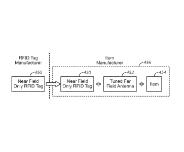
Referring next to FIG. 4E, an illustration is shown of a decoupled
manufacturing process in accordance with several embodiments. Initially, a
near field
only RFID tag 450 (e.g., near field only RFID tags 200, 205) is obtained from
an
RFID tag manufacturer. The near field only RFID tag 450 is mass produced and
item
neutral. That is, the near field only RFID tag 450 has not been designed to
account
for the dielectric properties of any particular item to be tagged. Like those
described
above, the near field only RFID tag 450 does not include a tag or far field
antenna,
and thus; is only readable in the near field of the operating reader
wavelengths. Since
the near field only RFID tag 450 does not have to be tuned or otherwise
account for a
particular item, the cost of the near field only RFID tag 450 can be
minimized. For
example, there is less metal used in the near field only RFID tag 450.
Additionally,
the RFID tag manufacturer need only manufacture, and the item manufacturer
need
only obtain, one version of the near field only RFID tag 450 produced in mass
for all
items to be tagged.
The item manufacturer obtains the near field only RFID tag 450 and uses it
together with a far field antenna 452 (generically, a conductive element)
tuned for the
particular item 454 to be tagged (to the extent tuning is needed) to produce a
tagged
item 456. Since the far field antenna 452 is designed by the item
manufacturer, and
may often be implemented as part of the packaging design, the cost of the
overall
RFID tag can be reduced and item-level tagging in a commercial retail
environment is
achievable. By tuning the far field antenna 452 to the item, the item
manufacturer is
able to create tagged items that will be within acceptable read requirements
required
by retailers or customers of manufacturer vendors. It has been found that
there is
great variability in the performance of RFID tags when implemented on final
items
that RFID tag manufacturers are not in the best position to understand. Thus,
in some
embodiments, the location of the tuning function is provided to the entity
that is in the
best position to understand and know the final intended use of the tag.
Additionally,
as illustrated in FIGS. 5-16, the design of the far field antenna 452 may be
developed
together with the item or its packaging. Several embodiments of the decouple
the
-22-
CA 02755089 2011-09-09
WO 2010/104991
PCT/US2010/026882
manufacturing and design of the near field RFID tag functionality and the far
field
antenna functionality in a way that can lead to efficiencies in manufacturing
costs and
improvements in read rates.
Referring next to FIG. 5, a cross sectional view is shown of one
implementation of a decoupled near field only RFID tag 200 and far field
antenna 302
as affixed to a portion 502 of an item in accordance with one embodiment.
Alternatively, near field only RFID tag 205, 450 or other near field only RFID
tag
could be used. The portion 502 of the item may be the item itself or the
packaging of
the item. In the illustration, the near field only RFID tag 200 is coupled to
an interior
surface 504 of the portion 502 with coupler 506, which may be embodied as a
sticker
or other structure. The far field antenna 302 is illustrated as being coupled
to the
exterior surface 508 of the portion 502 of the item. In one embodiment, the
far field
antenna 302 is coupled to the portion 502 with couplers 510, 512. It is noted
that in
some embodiments, one or more of the couplers 506, 510 and 512 should be
insulating to prevent electrical coupling of the far field antenna and the
near field only
RFID tag. Other embodiments may allow the far field antenna 302 and the near
field
only RFID tag 200 to be electrically connected and magnetically coupled. In
one
embodiment, the couplers 510, 512 take the form of a sticker. Thus, a coupling
structure is provided to couple the far field antenna 302 and the near field
RFID tag
200 to the item in close proximity to ensure magnetic coupling therebetween
(or
capacitive coupling in the case of the near field only RFID tag 205). In
alternative
embodiments, the coupling structure provides an air gap separation between the
far
field antenna 302 and the near field only RFID tag 200. The portion 502 is
selected to
have a thickness to allow the close coupling, e.g., less than about 1/4 inch,
less than
about 1/8 inch, or less than about 1/16 inch. Alternatively, in one
embodiment, one or
both of the couplers 510 and 512 are not needed and the far field antenna 302
is
applied or printed directed to the surface 508. In this case, the surface 508
and the
portion 502 become the coupling structure to maintain the far field antenna
and the
near field only RFID tag in close proximity for electrical, magnetic and /or
capacitive
coupling. In the illustrated embodiment, the coupler 512 is removable from the
coupler 510 to allow the far field antenna 302 to be later removed depending
on the
use of the RFID tag. For example, a user could pull a tab 514 to remove the
coupler
-23-
CA 02755089 2011-09-09
WO 2010/104991
PCT/US2010/026882
512 and the far field antenna 302 from the coupler 510 and the portion 502.
Removal
of the coupler 512 results in the far field antenna being magnetically
decoupled from
the near field only RFID tag such that the remaining RFID tagged item will
only
function as a near field tag. That is, the proximity relationship between the
far field
antenna and the near field only RFID tag is removed. It is noted that the
coupler 510
may not be present or may be a layer of adhesive in other embodiments. In
another
alternative, the coupler 512 may simply take the form of an outer packaging
wrap,
such as a plastic or paper (preferably an insulating material) wrap having the
far field
antenna attached thereto, but removable when the plastic wrap is removed.
Referring next to FIG. 6, a cross sectional view is shown of another
implementation of a decoupled near field only RFID tag 200 and far field
antenna 302
as affixed to a portion 602 of an item in accordance with one embodiment. In
another
embodiment, near field only RFID tag 205, 450 or other near field only RFID
tag
could be used. The portion 602 of the item may be a portion of the item itself
or the
packaging of the item. In the illustration, the near field only RFID tag 200
is
embedded within layers of the portion 602, e.g., between layers of a
corrugated
cardboard structure, with coupler 604, which may be embodied as a sticker or
other
insulating structure. The far field antenna 302 is illustrated as being
coupled directly
to the exterior surface 606 of the portion 602 of the item with coupler 608.
In one
embodiment, the coupler 608 takes the form of a sticker. Thus, in some
embodiments, a coupling structure is provided to couple the far field antenna
302 and
the near field only RFID tag 200 to the portion 602 of the item in close
proximity to
ensure magnetic coupling therebetween without electrical coupling (or
capacitive
coupling in the case of the near field only RFID tag 205). The portion 602 is
selected
to have a thickness to allow the close coupling needed for magnetic or
inductive
coupling, e.g., less than about 1/4 inch, less than about 1/8 inch, or less
than about
1/16 inch. Again, in some embodiments, the far field antenna 302 and the near
field
only RFID tag 200 are electrically and magnetically coupled. In alternative
embodiments, the coupling structure provides an air gap separation between the
far
field antenna 302 and the near field only RFID tag 200. Alternatively, in one
embodiment, the far field antenna 302 is adhered or printed to the exterior
surface 606
such that the coupler 608 is not needed. In this case, the exterior surface
606 and the
-24-
CA 02755089 2011-09-09
WO 2010/104991
PCT/US2010/026882
portion 602 become the coupling structure to maintain the far field antenna
and the
near field only RFID tag in close proximity for electrical, magnetic and/or
capacitive
coupling. Although not specifically illustrated, in some embodiments, the
coupler
608 and the far field antenna 302 may be adapted to be removed from the
portion 602
to allow the far field antenna 302 to be later removed depending on the use of
the
RFID tag. For example, a user could pull on a tab to remove the coupler 609
and the
far field antenna 302. This removal will result in the far field antenna being
magnetically decoupled from the near field only RFID tag such that the
remaining
RFID tagged item will only function as a near field tag and no longer function
as a far
field tag. That is, the proximity relationship (whether electrical, magnetic
and/or
capacitive) between the far field antenna and the near field only RFID tag is
removed.
In one alternative, the coupler 608 may simply take the form of an outer
packaging
wrap, such as a plastic wrap, shrink wrap or paper wrap having the far field
antenna
attached thereto, but removable when the wrap is removed.
FIG. 7 is a cross sectional view of a further implementation of a decoupled
near field only RFID tag 200 and far field antenna 302 as affixed to a portion
702 of
an item in accordance with one embodiment. In another embodiment, near field
only
RFID tag 205, 450 or other near field only RFID tag could be used. The portion
702
of the item may be a portion of the item itself or the packaging of the item.
In the
illustration, the near field only RFID tag 200 is coupled to an exterior
surface 704 of
the portion 702 with the coupler 506, which may be embodied as a sticker or
other
structure. The far field antenna 302 is illustrated as being coupled to the
interior
surface 706 of the portion 702 of the item, e.g., it is printed or formed or
otherwise
adhered to the interior surface 706. In an alternative embodiment, the far
field
antenna 302 is coupled to the interior surface 706 with a coupler, such as a
sticker or
other structure. Thus, in some embodiments, a coupling structure is provided
to
couple the far field antenna 302 and the near field only RFID tag 200 to the
item in
close proximity to ensure magnetic coupling therebetween (or capacitive
coupling in
the case of the near field only RFID tag 205). The portion 702 is selected to
have a
thickness to allow the close coupling, e.g., less than about 1/4 inch, less
than about 1/8
inch, or less than about 1/16 inch. Again, in some embodiments, the far field
antenna
302 and the near field only RFID tag 200 are electrically and magnetically
coupled.
-25-
CA 02755089 2011-09-09
WO 2010/104991
PCT/US2010/026882
In alternative embodiments, the coupling structure provides an air gap
separation
between the far field antenna 302 and the near field only RFID tag 200. In the
illustrated embodiment, the coupler 506 is removable from the exterior surface
704 to
allow the near field only RFID tag 200 to be later removed depending on the
use of
the RFID tag. For example, a user could pull on the tab 514 to remove the
coupler
506 and the near field only RFID tag 200. Removal of the coupler 506 and near
field
RFID tag 200 results in the far field antenna being magnetically decoupled
from the
near field only RFID tag such that the far field RFID tagging of the item is
now
disabled. That is, the proximity relationship (whether electrical, magnetic
and/or
capacitive depending on the tag) between the far field antenna and the near
field only
RFID tag is removed. It is noted that the same or a different near field only
RFID tag
and coupler 506 could be positioned in place on the exterior surface 704
(i.e., the
proximity relationship is re-established) and then the item would be tagged
with a tag
operational and readable in both the near field and the far field. It is noted
that the
coupler 506 may not be present in some embodiments, and that the near field
only
RFID tag is attached with adhesive or other coupling structure to the exterior
surface
704. In another alternative, the coupler 506 may simply take the form of an
outer
packaging wrap, such as a plastic wrap having the near field only RFID tag
attached
thereto, but removable when the plastic wrap is removed.
Referring next to FIG. 8, a cross sectional view is shown of another
implementation of a decoupled near field only RFID tag 200 and far field
antenna 302
as affixed to a portion 802 of an item in accordance with one embodiment. In
another
embodiment, near field only RFID tag 205, 450 or other near field only RFID
tag
could be used. The portion 802 of the item may be a portion of the item itself
or the
packaging of the item. In the illustration, the far field antenna 302 is
coupled to an
exterior surface 804 of the portion 802, e.g., it is adhered, printed, or
otherwise
attached. The near field only RFID tag 200 is illustrated as being coupled in
proximity to the far field antenna 302 via coupler 806, which at least forms
an
electrical insulator or barrier between the far field antenna 302 and the near
field only
RFID tag 200 to prevent electrical contact. In the illustrated embodiment, the
coupler
806 completely surrounds the near field only RFID tag 200. In an alternative
embodiment, a sticker completely covers the far field antenna 302 and the near
field
-26-
CA 02755089 2011-09-09
WO 2010/104991
PCT/US2010/026882
only RFID tag 200. For example, the far field antenna and the near field only
RFID
tag are formed or positioned on the under side of a sticker. Thus, in some
embodiments, a coupling structure (surface 804 and coupler 806) is provided to
couple the far field antenna 302 and the near field only RFID tag 200 to the
item in
close proximity to ensure magnetic coupling therebetween (or capacitive
coupling in
the case of the near field only RFID tag 205). In preferred form, the portion
of the
coupler 806 that separates the far field antenna from the near field only RFID
tag is
selected to have a thickness sufficient to allow the close coupling, e.g.,
less than about
1/4 inch, less than about 1/8 inch, or less than about 1/16 inch. Again, in
some
embodiments, the far field antenna 302 and the near field only RFID tag 200
are
electrically and magnetically coupled, whereas in other embodiments they are
capacitively coupled together. In one alternative, such as illustrated in FIG.
9, an air
gap 902 is maintained between the near field only RFID tag 200 and the far
field
antenna 302 to prevent electrical coupling rather than using an insulating or
electrically non-conducting material, such as coupler 806. In the illustrated
embodiment, the coupler 806 is adapted to be removable from the exterior
surface of
the far field antenna 302 depending on the use of the RFID tag. For example, a
user
could pull on the tab 514 to remove the coupler 806 and the near field only
RFID tag
200. Removal of the coupler 806 and near field only RFID tag 200 results in
the far
field antenna being magnetically decoupled from the near field RFID tag such
that the
far field RFID tagging of the item is now disabled. That is, the proximity
relationship
(whether electrical, magnetic and/or capacitive depending on the tag) between
the far
field antenna and the near field only RFID tag is removed. It is noted that
the same or
a different near field only RFID tag and coupler 806 could be positioned in
place on
the exterior surface 804 (i.e., the proximity relationship is re-established)
and then the
item would be tagged with a tag operational and readable in both the near
field and
the far field. In an alternative, the coupler 806 may simply take the form of
an outer
packaging wrap, such as a plastic or paper wrap having the near field only
RFID tag
attached thereto, but removable when the wrap is removed.
Referring next to FIG. 14, a cross sectional view is shown of another
implementation of a decoupled near field only RFID tag 200 and far field
antenna 302
as affixed to portion 802 of an item in accordance with one embodiment. This
-27-
CA 02755089 2011-09-09
WO 2010/104991
PCT/US2010/026882
embodiment is similar to the embodiment of FIG. 8 and its variations, except
that the
coupler 1406 allows for the near field only RFID tag 200 to electrically
contact the far
field antenna 302. Thus, the far field antenna 302 is electrically and
magnetically
coupled to the near field only RFID tag. In other words, the far field antenna
302 is
coupled in proximity to the near field only RFID tag. Similar to coupler 806,
coupler
1406 is adapted to be removable from the exterior surface of the far field
antenna 302.
For example, a user could pull on the tab 514 to remove the coupler 1406 and
the near
field only RFID tag 200. Removal of the coupler 1406 and near field only RFID
tag
200 results in the far field antenna being electrically and magnetically
decoupled from
the near field only RFID tag such that the far field RFID tagging of the item
is now
disabled. That is, the proximity relationship (electrical and magnetic)
between the far
field antenna and the near field only RFID tag 200 is removed. It is noted
that the
same or a different near field only RFID tag and coupler 1406 could be
positioned in
place on the exterior surface 804 (i.e., the proximity relationship is re-
established) and
then the item would be tagged with a tag operational and readable in both the
near
field and the far field. In an alternative, the coupler 1406 may simply take
the form of
an outer packaging wrap, such as a plastic or paper wrap having the near field
only
RFID tag attached thereto, but removable when the wrap is removed.
Accordingly, several examples are provided for various coupling
configurations to locate the near field only RFID tag and the far field
antenna such
that they are coupled in proximity, or have a proximity relationship
therebetween. For
example, one some cases, the near field only RFID tag and the far field
antenna are
coupled in proximity to ensure magnetic coupling but not electrical contact.
In other
embodiments, the various coupling configurations can locate the far field
antenna
such that it is in electrical connection with one or more of the near field
only RFID
tag, the loop and the integrated circuit of the near field only RFID tag so
that the near
field only RFID tag is electrically and magnetically coupled to the far field
antenna.
In other embodiments, the various coupling configurations can locate the far
field
antenna such that it is capacitively coupled with the near field only RFID
tag.
Examples of coupling structures include, but are not limited to, removable
materials,
stickers, labels, portions of the item or its packaging, other holding
structures to hold
the near field only RFID tag and the far field antenna in a fixed arrangement
but with
-28-
CA 02755089 2011-09-09
WO 2010/104991
PCT/US2010/026882
an air gap or insulator separation therebetween or electrical connection
therebetween,
to name a few. Furthermore, the coupling structures may include more than one
physical component. Coupling structures may also be insulating or non-
electrically
conducting materials. Additionally, the coupling structures may be configured
such
that one or both of the near field RFID tag and the far field antenna can be
removed
from close proximity or electrical connection to the each other, i.e., the
proximity
relationship is removed. This is in contrast to know integrated RFID tags
where the
near field tag and the far field antenna are non-separably integrated into a
single
integrated unit.
Referring next to FIG. 10, an illustration is shown of a portion of an item
packaging in which a far field antenna 302 is formed on a surface of the item
packaging and separate from the manufacturing of the near field only RFID tag
(such
as tags 200, 205 or 450) in accordance with one embodiment. In this
embodiment,
one surface (e.g., an inner surface) of the item to be tagged has a thin metal
layer 1002
or film (such as may be found in the material forming a bag of potato chips).
The
metal layer 1002 is deposited or printed on the plastic sheet of the item. In
accordance with one embodiment, the far field antenna 302 is etched or printed
into
the metal layer. In a further embodiment, the thin metal layer 1002 may be
printed as
a conductive printable ink or foil stamp. For example, as illustrated, the
metal layer
1002 is applied everywhere except about a periphery 1004 to form the far field
antenna 302. The result is that the elongated conductive strip formed within
the
periphery 1004 is used as the far field antenna. Prior testing indicates the
proper
dimensions of the far field antenna in order that it be tuned to the item
being tagged (if
additional dielectric tuning is needed) so that the RFID tag will work
properly. At
this point, a pre-manufactured near field only RFID tag can be located on the
opposite
or exterior side of the item in a location at a central portion of the far
field antenna
302 and to ensure proximity coupling (electrical and/or magnetic or capacitor
coupling). In other cases, the near field only RFID tag can be located on top
of the far
field antenna 302 at a central portion to ensure proximity coupling, e.g.,
using a
coupling structure such as a sticker, adhesive, etc. In this way, the far
field antenna
and the near field only RFID tag function in both the near field and the far
field.
Referring next to FIG. 15, an illustration is shown of a portion of an item
-29-
CA 02755089 2011-09-09
WO 2010/104991
PCT/US2010/026882
packaging in which the far field antenna 302 is formed on a surface of the
item
packaging in accordance with a variation of the embodiment of FIG. 10. This
embodiment is similar to FIG. 10 except that the far field antenna 302 is
formed with
the thin metal layer surrounding the periphery 1004. Electrons are caused to
move
about the periphery 1004 which causes a difference in potential voltage across
between the two elongated lengths of the periphery 1004. This is used to cause
current to occur in the loop of a near field only RFID tag. A pre-manufactured
near
field only RFID tag can be removably or non-removably coupled in proximity
(electrical and/or magnetic or capacitor coupling) to the far field antenna
302. In this
way, the far field antenna and the near field only RFID tag function in both
the near
field and the far field. The embodiment of FIG. 16 illustrates the proximity
coupling
of the near field only RFID tag 205 ensuring a capacitive coupling between the
tag
205 and the far field antenna.
It is noted that FIGS. 5-10 and 14-16 illustrate several different features of
several embodiments, and that it is understood that while not all combinations
of
features are described, one of skill in the art can incorporate or combine one
or more
features from one of more of the embodiments of FIGS. 5-10 and 14-16 to create
a
device in accordance with one or more embodiments of the invention.
Many of the embodiments described herein provide the decoupling of the
manufacturing of the near field only RFID tag and the far field antenna in an
RFID
device. In many cases, this results in a dramatic reduction in costs a
supplier must
bear to ensure item level tagging while meeting tag certifications. For
example, by
using a design in which all tags can use the same basic near field only RFID
tag, such
near field only RFID tags 200 and 205, regardless of the item being tagged,
the
supplier can achieve great economies of scale since such pre-manufactured near
field
tags can be ordered in bulk. Furthermore, the supplier will have lower costs
in
designing the far field antennas in many cases if simple conductive wiring is
used or
if integrated with label or packaging design. Accordingly, it is believed that
this
reduction is cost should make it much more cost effective and feasible to
implement
item level tagging.
Next, referring to FIGS. 11-13, illustrations are shown of example items to
incorporate RFID tagging devices wherein the far field antenna design is
incorporated
-30-
CA 02755089 2011-09-09
WO 2010/104991
PCT/US2010/026882
into the product label design in accordance with several embodiments. In the
illustration of FIG. 11, the material used to make the labeling of the package
includes
a metallic component which may be used to incorporate the far field antenna.
For
example, the label in this case includes a metal or conductive material.
Alternatively,
the label could include a printable conductive ink or a foil stamp or other
thin metallic
or conductive layer. Locations 1102 and 1104 provide example locations where a
far
field antenna may be implemented. Both locations 1102 and 1104 are generally
linear
and suitable to form the far field antenna. It is understood that the far
field antenna is
not required to be a straight linear structure in all embodiments, but is
shown so here
for simplicity. That is, it is understood that the far field antenna may be
implemented
in other non-linear arrangements or linear arrangements that change directions
or bend
around aspects of the label. Should location 1102 or 1104 be implemented as a
far
field antenna, the near field only RFID tag could be located on top of a
central portion
of the location or underneath a central portion of the location to provide
magnetic
coupling. Alternatively, the near field only RFID tag could be located on top
of an
end portion of the location or underneath an end portion of the location to
provide
efficient capacitive coupling. In FIG. 12, location 1202 is the left vertical
edge of the
Nutritional Facts product label printed on the item, which is a plastic
bottle. The edge
of the Nutritional Facts label could be printed with a conductive ink or a
foil stamp at
location 1202 (or about its entire periphery) and the near field only RFID tag
could be
located on top of the location 1202 or underneath it (inside the bottle) using
a sticker
or other adhesive material, for example. In a further example, FIG. 13
illustrates a
cardboard box package and includes example linear locations 1302, 1304 and
1306 as
possible locations to implement a far field antenna in the labeling of the
item. Again,
the far field antenna may be printed with conductive ink or have a foil stamp
applied
thereto during design and manufacture of the labeling/cardboard box. These
locations
are certainly not the only locations to implement a far field antenna, and are
provided
by way of example. This is important for some embodiments in that it allows
the item
manufacturer to design the far field antenna together with the product or
label design
(such as described in some embodiments of FIG. 4C) and allow use of standard,
low
cost pre-manufactured near field only RFID tags. This provides added
flexibility and
new efficiencies for suppliers to provide cost effective item level tagging.
-31-
CA 02755089 2011-09-09
WO 2010/104991
PCT/US2010/026882
Referring next to FIG. 17, a flowchart of the steps performed in one or more
manufacturing methods in accordance with several embodiments. Embodiments of
the methods of FIG. 17 may be used to manufacture one or more of the RFID tag
devices and other RFID tag devices as described herein.
Initially, a near field only RFID tag that does not function as a far field
tag is
obtained (Step 1702). In some embodiments, the near field only RFID 200, 205
and/or 450 may be used. In several embodiments, the near field only RFID tag
includes an integrated circuit or chip and a near field loop, but does not
include a tag
antenna or far field antenna. In one embodiment, the near field only RFID tag
is
obtained by removing the far field antenna from a commercially available
integrated
near and far field RFID tag. In another embodiment, such as described in FIG.
4E, for
example, the near field only RFID tag is manufactured in mass by an RFID tag
manufacturer. In some embodiments, the near field only RFID tag is not
designed to
account for the dielectric properties of any particular item to be tagged.
Next, a conductive element is tuned to an item to be tagged, where the
conductive element is adapted to function as a far field antenna (Step 1704).
In some
embodiments, this is done in a separate manufacturing process, for example, by
an
item or packaging manufacturer or packager, such as described in connection
with
FIG. 4E. This tuning accounts for the particular dielectric properties of the
item to be
tagged, or product attached to the item (product label) actually tagged. When
referring to the tuning of the conductive element, generally, one purpose of
the RFID
tag device is to provide an impedance matching structure to couple
electromagnetic
energy (e.g., radio frequency) in free space to an integrated circuit
containing the
integrated circuit or chip. The dielectric properties of the item to be tagged
can alter
the impedance match of the RFID tag device such that the conductive element
(e.g.,
far field antenna) may become de-tuned. This can result in read errors. Thus,
tuning
can be referred to as impedance matching. An effect of being substantially
tuned is
that the RFID device will perform substantially efficiently as a far field
device. By
designing the conductive element (for example, designing its dimensions), the
conductive element can be tuned to a particular item. In some embodiments,
this
tuning is done by trimming the length of the conductive element while being
influenced by the dielectric of the target item (or otherwise printing various
-32-
CA 02755089 2011-09-09
WO 2010/104991
PCT/US2010/026882
dimensioned conductive elements) until an optimal impedance match is found. In
one
embodiment, through testing, different dimensions of the conductive element
are used
and an optimal tuned dimension results when the performance of the RFID tag
sensitivity and backscatter strength on either side of the dimension drops. In
several
embodiments, advantageously, the near field only RFID tag is not required to
be
tuned and thus, can be cost effectively mass produced, whereas the conductive
element is tuned to the item in a separate manufacturing process. In some
embodiments, this step is optional if tuning is not required for a particular
item to be
tagged.
Next, the near field only RFID tag and the conductive element are coupled to
the item such that the near field only RFID tag and the conductive element are
coupled in proximity to each other so that the RFID tag will function in both
the near
field and far field (Step 1706). This may be done in any variety of ways and
implemented by a variety of coupling structures, couplers and/or surfaces,
such as
described and illustrated herein. For example, in one embodiment, the
conductive
element is formed from a printable conductive ink that is printed to a surface
of the
item (or its packaging). In another embodiment, the conductive element is
formed or
applied using a foil stamp to a surface of the item (or its packaging).
Additionally, in
one embodiment, the conductive element is located relative to the near field
RFID tag
such that the conductive element is magnetically coupled to the near field
only RFID
tag. In another embodiment, the conductive element is located relative to the
near
field RFID tag such that the conductive element is capacitively coupled to the
near
field only RFID tag. In a further embodiment, the conductive element is
located
relative to the near field RFID tag such that the conductive element is
electrically
contacting the near field only RFID tag.
Next, in accordance with some embodiments, one of the near field only RFID
tag and the conductive element are decoupled from the item, the near field
only RFID
tag and the conductive element no longer coupled in proximity to each other
such that
the RFID tag no longer functions or is readable in the far field (Step 1708).
In some
embodiments, this is illustrated in simplified form in FIG. 3B and 3E. This
may be
done in any variety of ways and implemented by a variety of coupling
structures,
couplers and/or surfaces, such as described and illustrated herein.
-33-
CA 02755089 2011-09-09
WO 2010/104991
PCT/US2010/026882
Next, in accordance with some embodiments, the one of the near field only
RFID tag and the conductive element (or a replacement or different one of the
near
field only RFID tag and the conductive element) is recoupled to the item, the
near
field only RFID tag and the conductive element again coupled in proximity to
each
other such that the RFID tag again functions in both the near field and the
far field
(Step 1710). In some embodiments, this is illustrated in simplified form in
FIG. 3C
and 3F. This may be done in any variety of ways and implemented by a variety
of
coupling structures, couplers and/or surfaces, such as described and
illustrated herein.
Accordingly, as exemplified by the examples described herein, several radio
frequency identification (RFID) devices are provided. In one embodiment, a
radio
frequency identification (RFID) device comprises an item having a first
location and a
second location, and one of a near field only RFID tag and a conductive
element
coupled to the first location of the item, wherein the near field only RFID
tag does not
function as a far field RFID tag, wherein the conductive element is adapted to
function as a far field antenna. The second location of the item is adapted to
receive
and allow to be coupled thereto the other of the near field only RFID tag and
the
conductive element, the second location located relative to the first location
such that
when the other of the near field only RFID tag and the conductive element is
coupled
thereto, the conductive element will be coupled in proximity to the near field
only
RFID tag such that the RFID device will function in both a near field and a
far field.
Additionally, various methods are provided to make a radio frequency
identification (RFID) device. In one embodiment, a method of making a radio
frequency identification (RFID) device comprises the steps: coupling a pre-
manufactured near field only RFID tag to an item, wherein the near field only
RFID
tag does not function as a far field RFID tag; and coupling a conductive
element to the
item, wherein the conductive element is adapted to function as a far field
antenna;
wherein the coupling steps result in that the near field only RFID tag is
located in a
proximity relationship to the conductive element such that the RFID device
functions
in both a near field and a far field; and wherein one of the coupling steps
comprises
removably coupling a respective one of the near field only RFID tag and the
conductive element to the item such that the proximity relationship between
the near
field only RFID tag and the conductive element may be later removed such that
the
-34-
CA 02755089 2011-09-09
WO 2010/104991
PCT/US2010/026882
RFID device no longer functions in the far field.
In another embodiment, a method of making a radio frequency identification
(RFID) device comprises the steps: coupling, in a first manufacturing process,
one of
a pre-manufactured near field only RFID tag and a conductive element to an
item,
wherein the near field only RFID tag does not function as a far field RFID
tag,
wherein the conductive element is adapted to function as a far field antenna;
and
coupling, in a second manufacturing process separate from the first
manufacturing
process, the other of the near field only RFID tag and the conductive element
to the
item, wherein the coupling steps result in that the near field only RFID tag
is located
proximate to and coupled in proximity to the conductive element such that the
RFID
device functions in both a near field and a far field.
Furthermore, the described features, structures, or characteristics of the
invention may be combined in any suitable manner in one or more embodiments.
In
the following description, numerous specific details are provided to provide a
thorough understanding of embodiments of the invention. One skilled in the
relevant
art will recognize, however, that the invention can be practiced without one
or more
of the specific details, or with other methods, components, materials, and so
forth. In
other instances, well-known structures, materials, or operations are not shown
or
described in detail to avoid obscuring aspects of the invention.
While the invention herein disclosed has been described by means of specific
embodiments, examples and applications thereof, numerous modifications and
variations could be made thereto by those skilled in the art without departing
from the
scope of the invention set forth in the claims.
-35-