Note: Descriptions are shown in the official language in which they were submitted.
CA 02755716 2011-09-16
WO 2010/105694 1 PCT/EP2009/053324
METHODS AND APPARATUSES FOR COMPENSATION OF I/Q
IMBALANCE
Technical Field
The present invention relates to methods and apparatuses for compensation of
imbalance between I (In-phase) and Q (Quadrature) signal paths in a quadrature
receiver
and a quadrature transmitter.
Background
Mismatch, or imbalance, between an in-phase (I) and a quadrature (Q) signal
path in a quadrature receiver circuit limits the achievable image attenuation,
which
results in a distorted signal. Likewise, imbalance between an I and a Q signal
path in a
quadrature transmitter circuit also poses a limitation on the achievable image
attenuation.
Various techniques have been developed for compensation of such imbalance
in order to mitigate the effects of the imbalance and provide improved image
attenuation. For example, the article L. Antilla et al, "Circularity-based I/Q
imbalance
compensation in wideband direct-conversion receivers", IEEE Transactions on
Vehicular Technology, vol. 57, no. 4, pp. 2099 - 2113, July 2008, discloses
compensation of I/Q imbalance in quadrature receivers. In the following, this
article is
referred to as the Antilla receiver paper. Furthermore, the article L. Antilla
et al,
"Frequency-selective I/Q mismatch calibration of wideband direct-conversion
transmitters", IEEE Transactions on Circuits and Systems IL: Express Briefs,
vol. 55,
no. 4, pp. 359-363, April 2008, discloses compensation of I/Q imbalance in
quadrature
transmitters. In the following, this article is referred to as the Antilla
transmitter paper
Fig. 1 illustrates a block diagram of a basic compensation circuit 1 utilized
in
both of the articles mentioned above. A complex-valued signal ol(n) is an
input signal
to the compensation circuit 1 and another complex-valued signal o2(n) is
output from
the compensation circuit 1. In the case of a receiver circuit, ol(n) is a
signal,
representing received data, having unbalanced I and Q components that is
processed by
the compensation circuit 1 to generate the signal o2(n) with (ideally)
restored balance
between the I and Q components. In the case of a transmitter circuit, oi(n) is
a signal,
CA 02755716 2011-09-16
WO 2010/105694 2 PCT/EP2009/053324
representing data to be transmitted, having balanced I and Q components, which
is
processed by the compensation circuit 1 to generate the signal o2(n) with
imbalance
between the I and Q components that compensates for the imbalance in the I and
Q
signal paths of the transmitter such that the transmitted radio-frequency (RF)
signal
(ideally) has balanced I and Q components. In either case, the signal ol(n) is
input to a
block 2 that generates the complex conjugate o; (n) of o1(n), which is
filtered by a filter
3 having the frequency response W(e' '). The output signal of the filter 3 is
added to the
signal ol(n) in the adder unit 4 to generate the signal o2(n).
It is desirable to provide efficient compensation of imbalance between I and Q
signal paths of a quadrature receiver or a quadrature transmitter at a
relatively low
computational complexity, e.g. in order provide a relatively small overhead in
terms of
required circuit area and/or power consumption for performing the
compensation.
Summary
An object of the present invention is to provide means for compensation of
imbalance between an in-phase (I) and a quadrature (Q) signal path of a
quadrature
receiver with a relatively low computational complexity. Another object of the
present
invention is to provide means for compensation of imbalance between an I and a
Q
signal path of a quadrature transmitter with a relatively low computational
complexity.
According to a first aspect, there is provided a method for compensating an
imbalance between an I and a Q signal path of a quadrature receiver adapted to
generate
a real-valued uncompensated digital I component a(n) and a real-valued
uncompensated
digital Q component b(n), together forming an uncompensated complex digital
signal
x(n) = a(n) +jb(n), wherein j denotes the imaginary unit and n is a sequence
index. The
method comprises generating a complex compensation signal by filtering one of
a(n)
and jb(n) with a compensation filter having a complex-valued impulse response.
Furthermore, the method comprises generating a first compensated complex
digital
signal as the sum of x(n) and the complex compensation signal.
The method may further comprise adaptively generating filter parameters of
the compensation filter.
CA 02755716 2011-09-16
WO 2010/105694 3 PCT/EP2009/053324
The impulse response of the compensation filter maybe on the form:
ho (n) + j (p8(n) + j rpho (n) + (e'(p -1- j (P) = (8(n) + ho (n)), wherein
6(n) is the unit pulse,
(p is a real-valued parameter and hA(n) is a real-valued sequence. Adaptively
generating
filter parameters of the compensation filter may comprise adaptively
generating the
real-valued parameter cp and the real-valued sequence hA(n).
Adaptively generating filter parameters of the compensation filter may
comprise, for each of a number of iterations, where each iteration is
identified by an
iteration index i, generating filter parameters for attaining an impulse
response f ')(n),
wherein f')(n) is a default impulse response for the first iteration, wherein
i = 1, and
f')(n) is based on f'-i)(n) and A('-i)(n) for i > 1, and A'i-1)(n) is an
estimated impulse-
response error of a preceding iteration. Furthermore, for each iteration,
adaptively
generating said filter parameters may comprise generating the complex
compensation
signal, denoted e(An), as e(')(n) = f')(n)*w(n), wherein * denotes the
convolution
operator and w(n) denotes said one of a(n) andjb(n). Moreover, for each
iteration,
adaptively generating said filter parameters may comprise generating the first
compensated complex digital signal, denoted v(')(n), as vP)(n) = x(n) +
e(')(n). In addition,
for each iteration, adaptively generating said filter parameters may comprise
generating
filter parameters determining A()(n) by minimizing a cost function based on
u(')(n) = v(')(n) + A(')(n)*w(n).
Said cost function may e.g. a linear cost function. Furthermore, said cost
function may be based on a properness measure of u(')(n).
Each iteration may further comprise generating a second compensated complex
digital signal y(')(n) = v('(n) + A()(n)*w(n) based on the generated A('(n).
The method may further comprise determining whether a condition for ending
said iterations is fulfilled. Moreover, the method may comprise, if said
condition is
fulfilled, ending said iterations and continuing compensating said imbalance
between
the I and the Q signal path based on filter parameters generated in the last
iteration.
The impulse response f {')(n) may be on the form:
f ") (n) = ho") (n) + j cp(k)8(n) + j p ' ho) (n) + (e'~"' -1- j X00 ). (8(n)
+ ho') (n)), wherein
CA 02755716 2011-09-16
WO 2010/105694 4 PCT/EP2009/053324
5(n) is the unit pulse, (p(') is a real-valued parameter and ho') (n) is a
real-valued
sequence.
Furthermore, A(')(n) may be on the form: A(') (n) = A" (n) + j") for n
h (P
belonging to a finite set of integers and A(') (n) = 0 outside said finite set
of integers,
wherein A') is a real-valued parameter and Ash) (n) is a real-valued sequence.
Generating filter parameters determining A(')(n) may comprise generating the
real-valued parameter A(') and the real-valued sequence A` (n) .
Generating filter parameters for attaining the impulse response f 'fi(n) may
comprise generating the real-valued sequence ho) (n) as ho') (n) = ho'-') (n)
+ A('-') (n)
and the real-valued parameter cp(') as ~90) = (P ('-') + A('') for i > 1.
According to a second aspect, there is provided a method for compensating an
imbalance between an I and a Q signal path of a quadrature receiver adapted to
generate
a real-valued uncompensated digital I component a(n) and a real-valued
uncompensated
digital Q component b(n), together forming an uncompensated complex digital
signal
x(n) = a(n) +jb(n), wherein j denotes the imaginary unit and n is a sequence
index. The
method comprises for each of a number of iterations, where each iteration is
identified
by an iteration index i, generating sample values of a finite-length real-
valued impulse
response g(A') (n) that can adopt nonzero values for n in a finite set K,
wherein go') (n) is
a default impulse response for the first iteration, wherein i = 1, and go (n)
is given by
go) (n) = go"-') (n) + A('-') (n) for i > 1, and A('-') (n) is an estimated
impulse-response
9 9
error of a preceding iteration. Furthermore, for each iteration, the method
comprises
generating a real-valued phase parameter (p(') as a default value for the
first iteration,
where i = 1, and as ~o(o = (P (1-1) + A('-') for i > 1, wherein Y-') is an
estimated phase-
(9 0
parameter error of the preceding iteration. Moreover, for each iteration, the
method
comprises generating a first compensated complex digital signal, denoted
v(An), as
W W go') (n) + 5(n)
v (n) = x(n) + tan(( )w, (n) + cos(+p- 8(n) * w2 (n), wherein * denotes
the convolution operator, and either wi(n)=
a(n) and w2(n) jb(n) or wi(n)=b(n) and
CA 02755716 2011-09-16
WO 2010/105694 5 PCT/EP2009/053324
w2(n)=a(n). In addition, for each iteration, the method comprises generating
the
estimated impulse response error A) (n) and the estimated phase-parameter
error A(')
by minimizing a cost function based on
u (') (n) = vW'W (n) + I (A) (k)w2 (n - k) + A') w, (n - k)).
kEK
Said cost function may be a linear cost function. Furthermore, said cost
function may be based on a properness measure of u(i)(n).
Each iteration may further comprise generating a second compensated complex
digital signal y(1) (n) = vW (n) + I (A') (k)w2 (n - k) + A(')w, (n - k))
based on the
keK
generated A!') (n) and A(')
The method may further comprise determining whether a condition for ending
said iterations is fulfilled. Furthermore, the method may comprise, if said
condition is
fulfilled, ending said iterations and continuing compensating said imbalance
between
the I and the Q signal path based on filter parameters generated in the last
iteration.
According to a third aspect, there is provided a signal-processing device for
compensating an imbalance between an I and a Q, signal path of a quadrature
receiver,
wherein the quadrature receiver is adapted to generate a real-valued
uncompensated
digital I component a(n) and a real-valued uncompensated digital Q component
b(n),
together forming an uncompensated complex digital signal x(n) = a(n) +jb(n),
wherein j
denotes the imaginary unit and n is a sequence index, wherein the signal-
processing
device (30) is adapted to receive the uncompensated digital signal x(n) and
compensate
said imbalance by performing the method according to the first or the second
aspect.
According to a fourth aspect, there is provided a quadrature receiver. The
quadrature receiver comprises an I and a Q signal path for generating a real-
valued
uncompensated digital I component a(n) and a real-valued uncompensated digital
Q
component b(n), together forming an uncompensated complex digital signal x(n)
= a(n)
+jb(n), wherein j denotes the imaginary unit and n is a sequence index.
Furthermore,
the quadrature receiver comprises a signal-processing device according to the
third
aspect for compensating an imbalance between the I and the Q signal path.
CA 02755716 2011-09-16
WO 2010/105694 6 PCT/EP2009/053324
According to a fifth aspect, there is provided a method for compensating an
imbalance between an I and a Q signal path of a quadrature transmitter
arranged to
transmit a radio-frequency signal ra(t) representing an uncompensated complex-
valued
digital signal z(n) = c(n)+jd(n), wherein j denotes the imaginary unit, n is a
sequence
index, c(n) is an uncompensated digital I component, and d(n) is an
uncompensated
digital Q component, by generating a compensated complex-valued digital signal
having a compensated digital I component, which is provided to the I signal
path and a
compensated digital Q component, which is provided to the Q signal path. The
method
comprises generating a complex compensation signal by filtering one of c(n)
and jd(n)
with a compensation filter having a complex-valued impulse response.
Furthermore, the
method comprises generating a first compensated complex digital signal as the
sum of
z(n) and the complex compensation signal.
The method may further comprise adaptively generating filter parameters of
the compensation filter.
The impulse response of the compensation filter may be on the form:
ho (n) + j(p8(n) + j (ph, (n) + (e'~O -1- j 0 = (8(n) + ho (n)), wherein 8(n)
is the unit pulse,
cp is a real-valued parameter and hA(n) is a real-valued sequence. Adaptively
generating
filter parameters of the compensation filter may comprise adaptively
generating the
real-valued parameter cp and the real-valued sequence hA(n).
Adaptively generating filter parameters of the compensation filter may
comprise, for each of a number of iterations, where each iteration is
identified by an
iteration index i, generating filter parameters for attaining an impulse
response f ')(n),
wherein f t')(n) is a default impulse response for the first iteration,
wherein i = 1, and
P')(n) is based on f{'-'k(n) and A(' ')(n) for i > 1, and A(' ')(n) is an
estimated impulse-
response error of a preceding iteration. Furthermore, for each iteration,
adaptively
generating said filter parameters may comprise generating the complex
compensation
signal, denoted e(An), as e(')(n) = f{')(n)*w(n), wherein * denotes the
convolution
operator and w(n) denotes said one of c(n) and jd(n). Moreover, for each
iteration,
adaptively generating said filter parameters may comprise generating the first
compensated complex digital signal, denoted v(An), as v(')(n) = x(n) +
e(')(n). In addition,
for each iteration, adaptively generating said filter parameters may comprise
generating
CA 02755716 2011-09-16
WO 2010/105694 7 PCT/EP2009/053324
filter parameters determining A(')(n) by minimizing a cost function based on a
real-
valued signal rBB(n), which is obtained from real downconversion of the signal
ra(t).
Said cost function may be a linear cost function. Furthermore, the method may
comprise generating a signal qBB(n) corresponding to a signal that would have
resulted
from real downconversion of a radio-frequency signal generated by inputting
the signal
z(t) to a quadrature transmitter having no imbalance between the I and Q
signal paths.
The cost function may be based on a difference between rBB(n) and qBB(n). For
example, the cost function is based on an L2 norm or L norm of said
difference.
Each iteration may further comprise generating a second compensated complex
digital signal y(')(n) = v(An) + A(')(n)*w(n) based on the generated A()(n).
The method may comprise determining whether a condition for ending said
iterations is fulfilled. Furthermore, the method may comprise, if said
condition is
fulfilled, ending said iterations and continuing compensating said imbalance
between
the I and the Q signal path based on filter parameters generated in the last
iteration.
The impulse response p')(n) may be on the form:
f (') (n) = ho') (n) + j ~9"'6(n) + j (p(')ho'~ (n) + (e'~`" -1- j rp(') )
(8(n) + ho') (n)), wherein
5(n) is the unit pulse, (p(') is a real-valued parameter and h(') (n) is a
real-valued
sequence.
Furthermore, A(An) may be on the form: Y) (n) = Ash' (n) + jA') for n
belonging to a finite set of integers and Y) (n) = 0 outside said finite set
of integers,
wherein Y(0) is a real-valued parameter and A(') (n) is a real-valued
sequence.
Generating filter parameters determining A(')(n) may comprise generating the
real-
valued parameter Y(0) and the real-valued sequence A(') (n) .
Generating filter parameters for attaining the impulse response f ')(n) may
comprise generating the real-valued sequence ho') (n) as ho') (n) = ho'-') (n)
+ Ash-') (n)
and the real-valued parameter cp(') as cp(') = (P ('-') + Y-') for i > 1.
According to a sixth aspect, there is provided a signal-processing device for
compensating an imbalance between an I and a Q signal path of a quadrature
transmitter
for transmitting a radio-frequency signal ra(t) representing an uncompensated
complex-
CA 02755716 2011-09-16
WO 2010/105694 8 PCT/EP2009/053324
valued digital signal z(n) = c(n)+jd(n), wherein j denotes the imaginary unit,
n is a
sequence index, c(n) is an uncompensated digital I component, and d(n) is an
uncompensated digital Q component. The signal processing device is adapted to
receive
the uncompensated complex-valued digital signal z(n) and generate a
compensated
digital I component, to be provided to the I signal path and a compensated
digital Q
component, to be provided to the Q signal path by performing the method
according to
the fifth aspect for compensating said imbalance.
According to a seventh aspect, there is provided a quadrature transmitter for
transmitting a radio-frequency signal ra(t) representing an uncompensated
complex-
valued digital signal z(n) = c(n)+jd(n). The quadrature transmitter comprises
an I and a
Q signal path arranged to receive a compensated digital I component and a
compensated
digital Q component, respectively, for generating the radio-frequency signal
ra(t).
Moreover, the quadrature transmitter comprises a signal-processing device
according to
the sixth aspect for compensating an imbalance between the I and the Q signal
path.
According to an eighth aspect, there is provided an electronic apparatus
comprising the quadrature receiver according to the fourth aspect and/or the
quadrature
transmitter according to the seventh aspect. The electronic apparatus may e.g.
be, but is
not limited to, a mobile communication terminal or a radio base station.
According to a ninth aspect, there is provided a computer program product
comprising computer program code means for executing the method according to
the
first, second, or fifth aspect when said computer program code means are run
by an
electronic device having computer capabilities.
According to a tenth aspect, there is provided a computer readable medium
having stored thereon a computer program product comprising computer program
code
means for executing the method according to the first, second, or fifth aspect
when said
computer program code means are run by an electronic device having computer
capabilities.
According to an eleventh aspect, there is provided a hardware-description
entity comprising computer-interpretable hardware-description code describing
the
signal-processing device according to the third or the sixth aspect and
enabling
CA 02755716 2011-09-16
WO 2010/105694 9 PCT/EP2009/053324
computer-aided fabrication thereof as an application-specific hardware unit,
through
configuration of a configurable hardware unit, or a combination thereof.
It is an advantage of embodiments of the present invention that imbalance
between an I and a Q signal path of a quadrature receiver or transmitter can
be
compensated at a relatively low overhead in terms of required computational
resources.
This, in turn, means that the required circuit area and/or power consumption
for
performing the compensation can be kept relatively low.
It should be emphasized that the term "comprises/comprising" when used in
this specification is taken to specify the presence of stated features,
integers, steps, or
components, but does not preclude the presence or addition of one or more
other
features, integers, steps, components, or groups thereof.
Brief Description of the Drawings
Further objects, features and advantages of embodiments of the invention will
appear from the following detailed description, reference being made to the
accompanying drawings, in which:
Fig. 1 is a block diagram of a known circuit for compensating I/Q imbalance;
Fig. 2 is a block diagram of a quadrature receiver according to an embodiment
of the present invention;
Fig. 3 is a block diagram of a model of a quadrature receiver circuit;
Figs. 4-7 are block diagrams of a signal-processing device according to
embodiments of the present invention;
Figs. 8-10 are flow charts for methods according to embodiments of the present
invention;
Fig. 11 is a block diagram of a signal-processing device according to an
embodiment of the present invention;
Fig. 12 is a flow chart for a method according to an embodiment of the present
invention;
Fig. 13 is a block diagram of a quadrature transmitter according to an
embodiment of the present invention;
Fig. 14 is a block diagram of a model of a quadrature transmitter circuit;
CA 02755716 2011-09-16
WO 2010/105694 10 PCT/EP2009/053324
Fig. 15 schematically illustrates an electronic apparatus according to an
embodiment of the present invention; and
Fig. 16 schematically illustrates a computer-readable medium and a
programmable hardware unit.
Detailed Description
Fig. 2 is a block diagram of a quadrature receiver 8 according to an
embodiment of the present invention. The quadrature receiver 8 is adapted to
receive a
continuous-time analog radio-frequency (RF) signal ra(t) on an input port 10.
In the
following, the subscript "a" is used together with signals and impulse
responses to
indicate that the signal/impulse response is an analog continuous-time
signal/impulse
response, t is used as a time variable indicating continuous time, and n is
used as a
sequence index indicating discrete time. Furthermore, reference is made in the
following to discrete-time signals/impulse responses that corresponds to
continuous-
time signals/impulse responses and vice versa. The term "corresponds" should
in these
contexts be interpreted as follows in this specification. In the case of a
discrete-time
signal s(n) that corresponds to a continuous-time signal sa(t), s(n) = sa(nT),
where T is
the sample period. It is assumed that the signal sa(t) is properly bandlimited
to allow
sampling without (significant) aliasing in accordance with the Nyquist
sampling
theorem. That is, it is assumed that the signal Sa(t) has no (or in practice,
only
negligible) spectral content at frequencies above a frequencyfBw < 1/(27). In
the case of
a discrete-time impulse response g(n) that corresponds to a continuous-time
impulse
response ga(t), the discrete-time Fourier transform G(e'') of g(n), defined by
G(e' T) _ Y~ g(n)e-is equal to the continuous-time Fourier transform Ga(jo))
of ga(t), defined by Ga (j w) = Jga (t)e-"dt for a relevant angular frequency
band, such
as 0 < w < n/T or a subset thereof.
According to the embodiment illustrated in Fig. 2, the quadrature receiver 8
comprises an in-phase (I) signal path 12a and a quadrature (Q) signal path
12b. The I
signal path 12a comprises a mixer 14a, and the Q signal path 12b comprises a
mixer
CA 02755716 2011-09-16
WO 2010/105694 11 PCT/EP2009/053324
14b. Both mixers 14a and 14b are adapted to receive the RF signal ra(t) on an
input port.
Furthermore, the quadrature receiver comprises a local oscillator (LO) unit
17, which is
adapted to generate LO signals to the mixers 14a and 14b. Ideally, the LO
signals
supplied to the mixers 14a and 14b are provided in quadrature, i.e., ideally,
there is a
90 (or it/2 radians) mutual phase shift between the LO signals. The mixers
14a and 14b
are arranged to perform frequency down conversion of a signal frequency band
of
interest of the RF signal ra(t) to a lower frequency range. In the following,
the
quadrature receiver 8 is assumed to be a direct conversion receiver, which is
adapted to
down convert said frequency band to a base band, i.e. to a frequency band
around 0 Hz.
In other words, the LO frequencyfo is a frequency band within said frequency
band of
interest. However, embodiments of the present invention is applicable to
quadrature
receivers that are adapted to down convert the signal frequency band of
interest to other
frequency bands as well.
According to the embodiment illustrated in Fig. 2, the quadrature receiver 8
further comprises a filter 20a and a filter 20b in the I signal path 12a and
the Q signal
path 12b, respectively. The filters 20a and 20b are arranged to suppress
unwanted
frequency components output from the mixers 14a and 14b. In Fig. 2, the
filters 20a and
20b are illustrated as low-pass (LP) filters. However, in other embodiments,
where the
quadrature receiver 8 is not a direct conversion receiver, the filters 20a and
20b may
instead be band-pass (BP) filters.
Moreover, in the embodiment illustrated in Fig. 2, the quadrature receiver 8
comprises an analog-to-digital converter (ADC) 25a and an ADC 25b in the I
signal
path 12a and the Q signal path 12b, respectively. The ADC 25a is adapted to
convert the
output signal from the filter 20a to a digital representation for generating a
real-valued
uncompensated digital I component, in the following denoted a(n). Similarly,
the ADC
25b is adapted to convert the output signal from the filter 20b to a digital
representation
for generating a real-valued uncompensated digital Q component, in the
following
denoted b(n). The real-valued signals a(n) and b(n) together form an
uncompensated
complex digital signal x(n) = a(n) +jb(n), wherein j denotes the imaginary
unit.
A problem with frequency down conversion using mixers is that a frequency
component of the input signal to the mixer located at a frequency fo + fl and
another
CA 02755716 2011-09-16
WO 2010/105694 12 PCT/EP2009/053324
frequency component of the input signal to the mixer located at a frequencyfo -
fi are
mapped onto the same frequencyfi in the output signal from the mixer. By means
of a
quadrature receiver configuration, wherein a complex-valued signal
representation is
used, it is possible to suppress one of the components (normally referred to
as the image
component), say the one atfo - f , and essentially maintain only the desired
component,
say the one atfo + fl. This is normally referred to as image rejection or
image
attenuation. In order to have a high degree of image attenuation, the I and Q
signal paths
need to be well balanced, i.e. the mutual phase difference between the LO
signals of the
I and Q signal paths needs to be close to 90 and the transfer functions of
the I and Q
signal paths need to be approximately equal. A mismatch, or imbalance, between
the I
and the Q signal path limits the achievable image attenuation. Such imbalance
is
normally due to temperature variations, manufacturing inaccuracies, and other
non-
idealities of the physical components in the I and Q signal paths of the
quadrature
receiver. Without use of compensation techniques, the achievable image
attenuation is
normally around 30 - 50 dB. Considering that the image component in some
situations
may well be 50 - 100 dB stronger than the desired component, such image
attenuation
may be insufficient.
To compensate for the problems with insufficient image attenuation, the
quadrature receiver 8 in the embodiment illustrated in Fig. 2 comprises a
signal-
processing device 30, which is adapted to compensate for imbalance between the
I
signal path 12a and the Q signal path 12b of the quadrature receiver 8. The
signal-
processing device 30 is adapted to receive the uncompensated digital signal
x(n) and
compensate said imbalance by performing a signal processing method, which is
further
described below in the context of various embodiments. Thereby, the resulting
overall
I/Q imbalance of the quadrature receiver 8 can be reduced compared with if the
signal-
processing device 30 had not been present.
In the embodiment illustrated in Fig. 2, the signal-processing device 30 is
adapted to receive the signal a(n) on an input port 32a and the signal b(n) on
an input
port 32d. Furthermore, the signal-processing device 30 is adapted to output a
compensated digital I component on an output port 34a and a compensated
digital Q
component on an output port 34b. In the embodiment illustrated in Fig. 2, the
signals
CA 02755716 2011-09-16
WO 2010/105694 13 PCT/EP2009/053324
a(n) and b(n) are the output signals from the ADCs 25a and 25b. However, in
other
embodiments, one or more intervening components (not shown) for generating the
signals a(n) and b(n) based on the output signals from the ADCs 25a and 25b
may be
connected between the ADCs 25a and 25b and the signal-processing device 30.
Nonlimiting examples of such intervening components may e.g. be filters or
components for performing sample-rate conversion, such as interpolation or
decimation.
Fig. 3 is a block diagram of a model of the quadrature receiver 8 in Fig. 2,
but
without the signal-processing device 30. The mixers 14a and 14b, and the LO 17
(Fig. 2) are modeled with the multipliers 40a and 40b multiplying the signal
ra(t) by
cos((oot+~oi) and -sin(c)ot+(P2), respectively, where wo is 27rfo. With
balanced I and Q
signal path, of = c2. A difference between cp1 and cp2 results in an imbalance
between the
I and Q signal paths.
The filters 20a and 20b (Fig. 2) are modeled with the blocks 45a and 45b,
respectively, having impulse responses hai (t) and hal(t), as indicated in
Fig. 3.
Furthermore, the ADCs 25a and 25b are modeled with ideal sample switches 50a
and
50b, respectively, arranged to sample the output signals from the blocks 45a
and 45b at
time instants t = nT, where T denotes the sample period, as illustrated in
Fig. 3. Any
gain mismatch between and (linear) dynamic behavior of the ADCs 25a and 25b
are
lumped into the blocks 45a and 45b in the model of Fig. 3.
An assumption used in derivations presented below is that the RF signal ra(t)
is
on the form ra (t) = za (t)e' 1 + za (t)e where za(t) is the corresponding
analog
representation of the discrete-time baseband signal z(n) = za (nT) = c(n) + jd
(n) , which
represents data transmitted by a transmitter, where c(n) and d(n) are both
real-valued
signals. A purpose of the quadrature receiver 8 is to enable recovery of said
data. The
signal x(n) can then be written on the form
x(n) = g, (n) * z(n) + g2 (n) * z* (n) , (Eq. 1)
where
e hl (n) + e->1'2 h2 (n)
g~ (n) = (Eq= 2)
2
CA 02755716 2011-09-16
WO 2010/105694 14 PCT/EP2009/053324
and
1", h,(n) - e M2 h2(n)
g2 (n) = e 2 (Eq 3)
Above, hi(n) and h2(n) are discrete-time impulse responses corresponding to
continuous-time impulse responses hal(t) and hal(t).
An equivalent representation is given by
x(n) = g, (n) * p(n) 92(n) * p* (n), (Eq= 4)
where the sign represents either + or - in different cases. In a case
referred to below as
case 1, + represents +, and in a case referred to below as case 2,
represents -. In Eq. 4,
g, (n) = 8(n) + 2 e h(n) (Eq= 5)
and
8(n) - e''h(n)
g2 (n) = 2 (Eq. 6)
According to case 1:
p(n) = e-iw, h, (n) * z(n), (Eq. 7)
h(n) * hi (n) = h2 (n) , (Eq. 8)
and
_ (P2 - ~01 (Eq.9)
According to case 2:
p(n) = e-'1' h2 (n) * z(n), (Eq. 10)
h(n) * h2 (n) = h, (n), (Eq. 11)
and
(P = (PI - (P2 (Eq.12)
CA 02755716 2011-09-16
WO 2010/105694 15 PCT/EP2009/053324
For both case 1 and case 2, the signal p(n) is a linearly distorted version of
z(n),
from which z(n) can be recovered by means of a linear equalizer. Such a linear
equalizer
is normally included in a receiver. Hence, the signal-processing device 30 can
be
adapted to recover p(n) instead of z(n), which can instead be recovered from
p(n) by
means of said equalizer. The real and imaginary part ofp(n) are in the
following
denoted ii(n) and b (n), respectively. Hence, p(n) = ii(n) + jb (n), where a
(n) and
b (n) are real-valued signals.
For case 1, we have:
x(n) = a(n) + j(cos((p)h(n) * b (n) - sin((p)h(n) * a(n)) (Eq. 13)
Similarly, for case 2, we have:
x(n) _ (cos(ip)h(n) * a(n) - sin(p)h(n) * b (n))+ jb (n) (Eq. 14).
It can be observed from Eq. 13 and Eq. 14 that the real and imaginary parts of
p(n) experience different transfer function, which results in image distortion
in the
signal x(n). Furthermore, it can be observed that in case 1, a(n) = a(n) (i.e.
the real
parts of x(n) and p(n) are equal), and in case 2, b(n) = b (n) (i.e. the
imaginary parts of
x(n) and p(n) are equal). This is utilized below in the derivation of resource-
efficient
circuitry and methods for compensating the I/Q imbalance.
In Figs. 4-7, referred to below, labels and reference signs included within
square brackets relate to embodiments of a corresponding signal processing
device for
compensating I/Q imbalance in a quadrature transmitter.
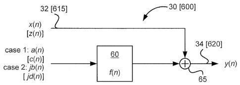
Fig. 4 is a block diagram of the signal-processing device 30 according to an
embodiment of the present invention. According to the embodiment, the signal-
processing device 30 comprises a compensation filter 60. The compensation
filter 60 is
arranged to receive an input signal having only a real or an imaginary
component, not
both. FurthenTnore, the compensation filter 60 has a complex-valued impulse
response,
and is therefore arranged to output a complex-valued output signal (i.e. a
signal having
both a real and an imaginary component), which is a compensation signal for
compensation of I/Q imbalance. In the embodiment of Fig. 1, the signal-
processing
CA 02755716 2011-09-16
WO 2010/105694 16 PCT/EP2009/053324
device 30 has an input port 32 and an output port 34. The input port 32 is a
compound
input port representing both input ports 32a and 32b in Fig. 2. Similarly, the
output port
34 is a compound output port representing both output ports 34a and 34b in
Fig. 2.
Furthermore, according to the embodiment illustrated in Fig. 4, the signal-
processing
device 30 comprises an adder unit 65 adapted to generate a complex compensated
digital signal y(n) as the sum of x(n) and the output signal of the
compensation filter 60.
The signal y(n) is output on the output port 34. With reference to Fig. 2, the
real part of
y(n) (or compensated digital I component) is output on the output port 34a,
and the
imaginary part ofy(n) (or compensated digital Q component) is output on the
output
port 34b.
For case 1, the compensation filter 60 is arranged to receive the real part
a(n)
of x(n) as an input signal. For case 2, the compensation filter 60 is arranged
to receive
the imaginary part b(n) of x(n), multiplied by j, as an input signal. Hence,
although such
a connection is not explicitly shown in Fig. 4, the compensation filter 60 may
be
operatively connected to the input port 32 for receiving its input signal. For
case 1, the
selection off(n) as
f (n) = e'lh(n) - 8(n) (Eq. 15)
results in
y(n) = cos((p)h(n) * p(n) = cos(rp2 - (o, )e-"' h2 (n) * z(n) (Eq. 16).
Hence, y(n) is a linear function of z(n), from which z(n) can be recovered by
means of a linear equalizer. Similarly, for case 2, the selection off(n) as
f (n) = e h(n) - 8(n) (Eq. 17)
results in
y(n) = cos(gp)h(n) * p(n) = cos(cp, - (P2)e-", h, (n) * z(n) (Eq. 18).
Hence, also for case 2, y(n) is a linear function of z(n), from which z(n) can
be
recovered by means of a linear equalizer.
It is an advantage of the embodiment illustrated in Fig. 4 that the same
performance in terms of image rejection can be achieved as for the
compensation circuit
CA 02755716 2011-09-16
WO 2010/105694 17 PCT/EP2009/053324
illustrated in Fig. 1 at a lower computational complexity, because only the
real or
imaginary part of x(n) is input to the compensation filter 60 in the
embodiment of
Fig. 4, whereas the filter 3 in the compensation circuit of Fig. 1 requires a
complex-
valued input signal. Hence, for a given performance in terms of image
attenuation, the
embodiment illustrated in Fig. 4 can be implemented using a smaller amount of
computational resources than the compensation circuit of Fig. 1. This, in
turn, can be
utilized to implement the embodiment of Fig. 4 with a lower power consumption
and/or
smaller circuit area than the compensation circuit of Fig. 1.
In order to facilitate efficient compensation of I/Q imbalance, filter
parameters
of the compensation filter 60 may be generated and updated adaptively. The
methods
disclosed in the Antilla receiver paper referred to in the "Background"
section can e.g.
be utilized for this purpose. Further approaches for adaptively generating
filter
parameters of compensation filters are disclosed below in the context of
certain
embodiments.
Further simplifications of the compensation filter 60 are possible, which
allows
for a further reduction of the required computational complexity, as is
disclosed below.
For case 1, f(n) can be rewritten as
f(n)= hA (n) + j (p8(n) + j cpho (n)
(Eq. 19)
+(e" -1- j(p).(8(n)+ho(n))
where ho (n) = h(n) - (5(n). A block diagram of an embodiment of the signal-
processing
device 30 that utilizes the expression of Eq. 19 for obtaining a computational-
efficient
implementation is illustrated in Fig. 5. In this embodiment, the signal-
processing device
comprises a filter unit 70 adapted to receive the real-valued signal a(n) as
an input
signal. The filter unit 70 has the impulse response hA(n). Furthermore, the
signal-
processing device 30 comprises an adder unit 75 adapted to generate the sum of
a(n)
and the output signal of the filter unit 70. In addition, the signal-
processing device 30
comprises a multiplication unit 80 adapted to multiply the sum generated by
the adder
unit 75 by the complex valued coefficient e' and output the generated
product.
Moreover, the signal-processing device 30 comprises an adder unit 85 adapted
to
generate the sum of said product output from the multiplication unit 80 and -
a(n). This
CA 02755716 2011-09-16
WO 2010/105694 18 PCT/EP2009/053324
sum corresponds to the complex-valued compensation signal output from the
compensation filter 60 in the embodiment illustrated in Fig. 4. The adder
circuit 85 is
further adapted to add said sum and the signal x(n) to form the compensated
digital
signal y(n). In a comparison between Figs. 4 and 5, the function of the
compensation
filter 60 (Fig. 4) is performed by the filter unit 70, multiplication unit 80,
and the adder
units 75 and 85 (Fig. 5), whereas the function of the adder unit 65 (Fig. 4)
is performed
by the adder unit 85 (Fig. 4).
The impulse responses f(n) and hA(n) have the same lengths. However,j(n) has
complex-valued samples, whereas hA(n) has only real-valued samples. In the
following,
it is assumed that the lengths off(n) and hA(n) are finite and equal to N
(i.e. finite-length
impulse response (FIR) filters are used for the compensation). If the
compensation filter
60 in the embodiment of Fig. 4 is implemented as an FIR filter of length N
with a "brute
force" approach (e.g. as a standard or transposed direct form FIR filter), N
multiplications with complex-valued coefficients are required for each sample,
which
corresponds to 2N multiplications with real-valued coefficients. With the same
"brute
force" approach used for implementing the filter unit 70 in Fig. 5, N
multiplications
with real-valued coefficients are required in the filter unit 70 for each
sample. In
addition, one multiplication with a complex-valued coefficient is required in
the
multiplication unit 80 for each sample, which corresponds to two
multiplications with
real-valued coefficients, resulting in a total of N+ 2 multiplications with
real valued
coefficients for each sample in the signal-processing device 30, which is
approximately
50 % of the number of multiplications for the case where the compensation
filter 60 of
Fig. 4 is implemented with a "brute force" approach. This can be utilized to
further
reduce the power consumption and/or the required circuit area. In addition,
the adaptive
generation of filter parameters is simplified, as only N real-valued filter
coefficients for
the filter unit 70 and the real-valued parameter cp need to be generated,
compared with N
complex-valued coefficients, corresponding to 2N real-valued coefficients,
which are to
be adaptively generated in the case where the compensation filter 60 of Fig. 4
is
implemented with the "brute force" approach.
Comparing Eq. 15 and Eq. 17, it is readily realized that the structure of the
signal-processing device 30 in Fig. 5 can be utilized also in case 2,
replacing a(n) with
CA 02755716 2011-09-16
WO 2010/105694 19 PCT/EP2009/053324
jb(n). This is illustrated in Fig. 5 with the label "case 2: jb(n)". Although
the parameter
cp enters with different signs in Eq. 15 and Eq. 17, this difference can be
compensated
for in the generation of the filter parameters by generating (p with different
signs in the
two cases (corresponding to a variable substitution where -(p is replaced with
(P in
Eq. 17). Such compensation is taken care of automatically in an adaptive
parameter-
generation scheme.
Adaptive generation of filter parameters in the signal-processing device 30
according to an embodiment of the present invention is described below with
reference
to Fig. 6. Fig. 6 is a block diagram of an embodiment of the signal-processing
device
30. According to this embodiment, the signal-processing device 30 comprises a
compensation filter 160a, which essentially corresponds to the compensation
filter 60 of
Fig. 4. The compensation filter 160a is arranged to receive an input signal
having only a
real or an imaginary component, not both. Furthermore, the compensation filter
160a
has a complex-valued impulse response, and is therefore arranged to output a
complex-
valued output signal, which is a compensation signal for compensation of I/Q
imbalance. Just as for the compensation filter 60 in Fig. 4, the compensation
filter 160a
is arranged to receive a(n) in case 1 and jb(n) in case 2, as is illustrated
in Fig. 6.
Filter parameters of the filter unit 160a are adaptively generated in a number
of
iterations. Each iteration is below identified by an iteration index i. For
the i:th iteration,
filter parameters for attaining an impulse response f ')(n) are generated. In
the first
iteration, f {')(n) maybe a default impulse response for the first iteration
(i.e. for i = 1).
The default impulse response may e.g. bef<')(n) = b(n). For the following
iterations (i.e.
for i > 1), ft')(n) is based on f {'-1)(n) and A('-i)(n), and A(' 1)(n) is an
estimated impulse-
response error of a preceding iteration. How f t')(n) can be based on f ti-1
)(n) and A('-')(n)
is described in more detail in the context of specific embodiments below.
Furthermore,
the complex compensation signal, which is denoted e(An) in the following, is
generated
on an output port of the compensation filter 160a as e(')(n) = f{')(n)*w(n),
wherein w(n)
denotes a(n) in case 1 and jb(n) in case 2. A first compensated complex
digital signal,
denoted v(An), is generated as v(An) = x(n) + e(An) in an adder unit 165a of
the signal-
processing device 30.
CA 02755716 2011-09-16
WO 2010/105694 20 PCT/EP2009/053324
In addition, filter parameters determining the estimated impulse response
error
A(')(n) are generated, which can be used in the (i + 1):th iteration for
determining')(n).
For example, the filter parameters determining A(')(n) may be generated based
on the
expression u(')(n) = v(')(n) + A(')(n)*w(n), using an optimization technique
aiming at
making the I/Q imbalance of u(')(n) lesser than that of v(')(n). For example,
the filter
parameters determining A(')(n) may be generated by minimizing a cost function
that is
based on u(')(n).
Assuming that the underlying signal z(t) is proper, as it is defined in the
Antilla
receiver paper referred to above, i.e. that
E[z(t)z(t - z-)] = 0 for all 'c, (Eq. 20)
where E[=] denotes the expectation value operator, the compensated signal
output from
the signal-processing device 30 should also be proper if the I/Q imbalance is
perfectly
compensated.
In such a case, the cost function based on u(1)(n) may be based on a
properness
measure of u(')(n). Such a properness measure P(A(')(n), k) may e.g. be
defined as
P(Y) (n), k) _ Y uO) (l)u(')(I - k), (Eq. 21)
lEL
where L is a suitably chosen interval. The length of L may e.g. be chosen
based on
computer simulations and/or measurements in order to obtain a desired accuracy
for a
given application. Furthermore, the cost function based on P(A(')(n), k) may
e.g. be
defined as
C(Y) (n)) Y (Re(P(A`'' (n), k)))2 + (Im(P(A`'' (n), k)))2 , (Eq. 22)
keK
where Re and Im denotes the real and imaginary parts, respectively, and K is a
suitably
chosen interval. The length of K may e.g. be chosen based on computer
simulations
and/or measurements in order to obtain a desired accuracy for a given
application. As a
general rule of thumb, the length of K should typically be at least of the
same order as
the length of A()(n).
The cost function C(A(')(n)) can be seen as a function of the filter
parameters
determining A(')(n). In the following discussion, the number of filter
parameters
CA 02755716 2011-09-16
WO 2010/105694 21 PCT/EP2009/053324
determining A(')(n) is denoted M. C(A(')(n)), as defined by Eq. 22, is
generally a
nonlinear cost function of the filter parameters determining A(')(n)
(depending, of
course, on how A(')(n) depends on the filter parameters). Another cost
function
C(Y) (n)) may be derived from the nonlinear cost function C(A()(n)) (defined
by
Eq. 22, or as a nonlinear cost function of the filter parameters in any other
suitable way)
by linearizing C(A(')(n)) with respect to the filter parameters, e.g. around
the point
A(')(n) = 0 for all n. Thereby, a linear cost function C(Y) (n)) in the M
filter parameters
is obtained. For example, a set of linear equations may be derived by
linearizing
(Re(P(A(' (n), k)))2 and (Im(P(AA') (n), k)))2 , with respect to the M filter
parameters, for
each k c K and setting the resulting linear equations equal to zero. Although
the filter
parameter values solving this linearized cost function does not exactly
correspond to the
minimum of C(A(')(n)), the solution to the linearized cost function will
normally, for
each iteration, successively approach a solution, or region of solutions,
close to the
optimum solution. An advantage of this approach is that it requires less
computational
resources than directly minimizing the nonlinear cost function C(A(')(n)).
As indicated in Fig. 6, the signal-processing device 30 may be further
arranged
to generate a second compensated complex digital signal y('(n) = v('(n) +
A()(n)*w(n)
based on the generated filter parameters determining A(')(n) (wherein, again,
w(n)
denotes a(n) in case 1 and jb(n) in case 2). For this purpose, the signal-
processing
device 30 may comprise a filter unit 160b, having the impulse response
A(1)(n), and an
adder unit 165b as indicated in Fig. 6. This second compensated digital signal
y(')(n)
may be the signal which is output on the output port 34. In other embodiments,
the
signal v(An) may instead be output on the output port 34. In such embodiments,
the
filter unit 160b and the adder unit 165b may be omitted.
In an embodiment, the compensation filter 160a is an FIR filter, wherein the
length of each of the impulse responses f ')(n) and A(')(n) are N.
Furthermore, the filter
parameters for attaining the impulse response f')(n) are the N real parts and
the N
imaginary parts of the samples of f')(n). Similarly, the filter parameters
determining
A(')(n) are the N real parts and the N imaginary parts of the samples of
A(')(n). Hence, in
CA 02755716 2011-09-16
WO 2010/105694 22 PCT/EP2009/053324
this embodiment, M = 2N. Moreover, in this embodiment, j')(n) is generated
based on
jt'-')(n) and A('-')(n) asft')(n) = ft'_')(n) + A('-1)(n)
Fig. 7 is a block diagram of another embodiment of the signal-processing
device 30, corresponding to the embodiment illustrated in Fig. 5, which also
illustrates
adaptive generation of filter parameters. In this embodiment, the impulse
response j ')(n)
is on the form
.f"(n) = ho''(n)+jq,(k)8(n)+jc ''ho''(n)
+(e'~`' 1- jrp('))=(8(n)+ho')(n)) (Eq. 23)
where cp(`) is a real-valued parameter and ho') (n) is a real-valued sequence.
This form of
f')(n) is motivated by Eq. 19.
In the embodiment illustrated in Fig. 7, the signal-processing device 30
comprises a filter unit 170, which essentially corresponds to the filter unit
70 in Fig. 5.
The filter unit 170 has the impulse response ho' (n) . Furthermore, the signal-
processing
device 30 comprises an adder unit 175 adapted to generate the sum of w(n)
(which, as
above, is used to denote a(n) for case 1 and jb(n) for case 2) and the output
signal of the
filter unit 170. The adder unit 175 essentially corresponds to the adder unit
75 in Fig. 5.
In addition, the signal-processing device 30 comprises a multiplication unit
180a
adapted to multiply the sum generated by the adder unit 175 by the complex
valued
coefficient e ""') and output the generated product. The multiplication unit
180a
essentially corresponds to the multiplication unit 80 in Fig. 5. Moreover, the
signal-
processing device 30 comprises an adder unit 185a adapted to generate the sum
of said
product output from the multiplication unit 180a and -w(n). The adder unit
185a
essentially corresponds to the adder unit 85 in Fig. 5. The output signal of
the adder unit
185a is a first compensated complex digital signal, denoted v(')(n).
For the embodiment illustrated in Fig. 7, the adaptive generation of filter
parameters may be performed in the same general way as described in the
context of
Fig. 6. The filter parameters detennining 4(')(n) may be a real-valued
parameter A(') and
a real-valued sequence A (n) , having the same length as the real-valued
sequence
CA 02755716 2011-09-16
WO 2010/105694 23 PCT/EP2009/053324
ho') (n) . The filter parameters to be generated for attaining the impulse
response f ')(n)
may be the real-valued sequence ho') (n), which can be generated as
h,,z) (n) = ho' ') (n) + Ash'_') (n) , (Eq. 24)
and the real-valued parameter cp('), which can be generated as
(p~') _ (p~' + (Eq. 25)
In the following, it embodiments where the filter unit 170a is an FIR filter
is
considered. Hence, the impulse response ho') (n) has finite length which is
denoted N in
conformity with the example above in connection with Fig. 6. The estimated
impulse
response error A(')(n) may be on the form
A~') (n) = A(') (n) + jA(' (Eq. 26)
for n belonging to a finite set of integers and A" (n) = 0 outside said finite
set of
integers. Said finite set of integers is the interval of length N for which
ho') (n) can
adopt nonzero values. The expression given by Eq. 26 is a first-order
approximation of
f"+ "(n) f ')(n) with f f')(n) given by Eq. 23 and (p(') and ho') (n) given by
Eq. 24 and
Eq. 25, respectively. For this situation, the number M of filter parameters
for attaining
the impulse response f {')(n) is N + 1, namely the N real-valued samples of
ho') (n) and
the real-valued parameter gyp('). For N> 1, this is less than for the example
presented
above with reference to Fig. 6, wherein M = 2N, whereby adaptive generation of
filter
parameters can be performed using less computational resources, which is an
advantage.
As indicated in Fig. 7, the signal-processing device 30 may be further
arranged
to generate a second compensated complex digital signal y(An) = v(')(n) +
A(')(n)*w(n)
based on the generated filter parameters determining A()(n). For this purpose,
the signal-
processing device 30 may comprise a filter unit 170b, having an impulse
response equal
to the real part of Eq 26, a filter unit 180b having an impulse response equal
to j
multiplied by the imaginary part of Eq. 26, and adder units 185b and 185c as
indicated
in Fig. 7. As for the embodiment illustrated in Fig. 6, this second
compensated digital
signal y(An) may be the signal which is output on the output port 34. In other
CA 02755716 2011-09-16
WO 2010/105694 24 PCT/EP2009/053324
embodiments, the signal v(')(n) may instead be output on the output port 34.
In such
embodiments, the filter units 170b and 180b and the adder units 185b and 185c
may be
omitted.
In a comparison between the block diagrams in Fig. 7 and the more general
block diagram of Fig. 6, the function of the compensation filter 160a (Fig. 6)
is
performed by the filter unit 170a, the multiplication unit 180a, and the adder
units 175
and 185a (Fig. 7). Furthermore, the function of the adder unit 165a (Fig. 6)
is performed
by the adder unit 185a (Fig. 7). Moreover, the function of the filter unit
160b (Fig. 6) is
performed by the filter units 170b and 180b and the adder unit 185b (Fig. 7),
and the
function of the adder unit 165b (Fig. 6) is performed by the adder unit 185c.
Fig. 8 is a flow chart of a method for compensating an imbalance between the I
signal path 12a and the Q signal path 12b of the quadrature receiver 8 (Fig.
2) according
to an embodiment of the present invention. The method may e.g. be performed by
the
signal-processing device 30 (Figs. 2-7). According to the embodiment, the
method is
started in step 200. In step 205, the uncompensated complex digital signal
x(n) = a(n) +jb(n) is received, e.g. on the input port 32 (Figs. 3-7) or ports
32a and 32b
(Fig. 2) of the signal-processing device 30. In step 210, the complex
compensation
signal is generated by filtering one of a(n) (case 1) and jb(n) (case 2) with
a
compensation filter having a complex-valued impulse response. Step 210 may
e.g. be
performed by the compensation filter 60 (Fig. 4), the elements 70-85 (Fig. 5)
described
above as performing the function of the compensation filter 60 (Fig. 4), the
compensation filter 160a (Fig. 6), or the elements 170a, 175, 180a, and 185a
(Fig. 7)
described above as performing the function of the compensation filter 160a
(Fig. 6).
Furthermore, in step 215, a first compensated complex digital signal is
generated as the
sum of x(n) and the complex compensation signal. Said first compensated
complex
digital signal may be the signal y(n) in Figs. 4 and 5, or the signal v(')(n)
in Figs. 6 and 7.
The method is ended in step 220.
The method may further comprise adaptively generating filter parameters of
the compensation filter. Adaptively generating filter parameters of the
compensation
filter may e.g. comprise adaptively generating the complex-valued samples of
the
impulse response f(n) or adaptively generating the real-valued samples of the
impulse
CA 02755716 2011-09-16
WO 2010/105694 25 PCT/EP2009/053324
response hA(n) and the real-valued parameter ~p as described above with
reference to
Figs. 4 and 5.
Fig. 9 is a flow chart indicating how adaptive generation of filter parameters
can be performed according to an embodiment of the present invention, which is
e.g.
applicable to the embodiments of the signal-processing device 30 illustrated
in Figs. 6
and 7. The flow chart in Fig. 9 illustrates one iteration of the iterative
process described
above with reference to Figs. 6 and 7. The iteration is started in step 300.
In step 305,
filter parameters for attaining the impulse response f')(n), wherein f ')(n)
is a default
impulse response for the first iteration, wherein i = 1, and f {')(n) is based
on f'-1)(n) and
A('-')(n) for i > 1. Furthermore, in step 310, the complex compensation
signal, denoted
e(An), is generated as e(An) = f')(n)*w(n), wherein w(n) denotes a(n) (case 1)
orjb(n)
(case 2). Moreover, in step 315, the first compensated complex digital signal
v(An) is
generated as v(')(n) = x(n) + e()(n). In addition, the filter parameters
determining A(')(n)
are generated in step 320 by minimizing a cost function based on
u(')(n) = v(An) + A(')(n)*w(n). The iteration is ended in step 320. In some
embodiments,
the iteration may also comprise generating a second compensated complex
digital signal
y(An) = v(An) + A(')(n)*w(n) based on the generated A(')(n) as described in
the context of
Figs. 6-7.
As described above with reference to Fig. 7, the cost function may be based on
a properness measure of u(')(n). Furthermore, as is also described in the
context of
Fig. 7, the cost function may be a linear cost function, such as a cost
function obtained
by linearization of a nonlinear cost function based on u('(n).
The impulse responses f{'(n) and A(')(n) may e.g. have any of the forms
described above in the context of Figs. 6 and 7 above. Furthermore, the steps
305 and
320 may e.g. comprise generating filter parameters in any of the ways
described above
with reference to Figs. 6 and 7.
In some embodiments, the iterations for adaptively generating filter
parameters
may be continually executed as long as the signal-processing device 30 is in
operation.
In other embodiments, the iterations may be terminated, or ended, when a
certain stop
condition for ending the iterations is fulfilled. Such a condition may e.g. be
that the
maximum value (over all n) of A' (n) is below a threshold value. The threshold
value
CA 02755716 2011-09-16
WO 2010/105694 26 PCT/EP2009/053324
may e.g. be selected based on a system specification, computer simulations
and/or
measurements, e.g. to achieve certain degree of image rejection required by
the system
specification or to fulfill some other criterion of system specification.
Such operation is illustrated by the flow chart in Fig. 10. In Step 400, the
operation is started. In step 405, it is determining whether the stop
condition is fulfilled.
If the stop condition is not fulfilled, the filter parameter generation is
iterated once more
in step 410. Step 410 may e.g. be performed in accordance with the flow chart
in Fig. 9.
If the stop condition is fulfilled, the iterations are ended and compensation
of the
imbalance between the I signal path 12a and the Q signal path 12b based on
filter
parameters generated in the last iteration is continued in step 415.
A slight modification of the block diagram of the signal processing device 30
in Fig. 6, resulting in essentially the same function, except for a phase
shift, at a
computational complexity that is comparable to that of the block diagram of
Fig. 6 is
shown in Fig. 11. The embodiment illustrated in Fig. 11 is motivated as
follows.
Setting, for case 1,
y(n) = x(n) + j tan((D)a(n) + cog (n) s(~p) - 8(n) * b(n) (Eq. 27)
or, for case 2,
y(n) = x(n) + tan((p)b(n) + cg(n) - 8(n) * a(n) (Eq. 28)
wherein, in both cases, g(n) * h(n) =6(n), then y(n) = p(n) for both cases.
That is,
y(n) is a linear function of z(n), from which z(n) can be recovered by means
of a linear
equalizer. The definitions for h(n) , p(n), and cp for the two cases are given
by Eq. 7 -
Eq. 11. Setting
go (n) = g(n) - 8(n), (Eq 29)
Eq. 27 can be rewritten as
CA 02755716 2011-09-16
WO 2010/105694 27 PCT/EP2009/053324
y(n) = x(n) + tan((p) ja(n)
+ ft go (n) + 8(n) - 8(n) * jb(n) (Eq. 30)
cos(rp)
and Eq. 28 can be rewritten as
y(n) = x(n) + tan(gp)b(n)
+ ftg) + 8(n) 8(n) * a(n) (Eq. 31)
cos(rp)
It should be noted that go (n) is a real-valued sequence.
According to the embodiment illustrated in Fig. 11, the signal processing
device 30 comprises a filter unit 500a, which is arranged to receive and
filter a signal,
which in the following is denoted w2(n). For case 1, w2(n) =jb(n), and for
case 2,
W2(n) = a(n) as indicated in Fig. 11. The filter unit 500a has a real-valued
finite-length
impulse response g(')
(n), which can adopt nonzero values for n in a finite set K. For
example, the set K may be an interval of length N, whereby go" (n) has a
finite length
N. Furthermore, the signal processing device comprises an adder unit 505
arranged to
generate the sum of the output signal of the filter unit 500a and w2(n).
Moreover, the
signal processing device 30 comprises a multiplication unit 510, which is
arranged to
multiply the sum generated by the adder unit 505 by a factor 1/cos(cp(')),
wherein (p(') is a
real-valued parameter.
According to the embodiment illustrated in Fig. 11, the signal processing
device 30 further comprises a multiplier unit 520, which is arranged to
multiply a signal
wi(n) by a factor tan(cp(')). In case 1, the signal wI(n) =ja(n), and in case
2, wi(n) = b(n),
as is illustrated in Fig. 11. Furthermore, the signal processing device 30
comprises adder
units 515a and 515b which are adapted to generate a first compensated complex
digital
signal v(')(n) as
v(') (n) = x(n) + tan(gp(') )w1 (n)
+ g(n) + '5(n))-,5(n) * w (Eq. 32)
cos(gp('' ) 2(n)
CA 02755716 2011-09-16
WO 2010/105694 28 PCT/EP2009/053324
A comparison between Eq. 32 and Eq. 30-31 provides a motivation for the
structure of the block diagram in Fig. 11. Similar to the adaptive generation
of filter
parameters described with reference to Figs. 6-7 and 9, the parameter P(I) and
sample
values of a go'~ (n) are adaptively generated in a number of iterations. Each
iteration is
identified below by the iteration index i. For the first iteration, wherein i
= 1, go'~ (n)
may be a default impulse response and gyp(') may be assigned a default value,
such as
go')
(n) = 0 and rp(') = 0. For subsequent iterations, i.e. for i > 1, go') (n) is
given by
9A (n) = go' (n) + A('-') (n) and cp(') is given by cp(') = rp~' + A('') ,
wherein A'K') (n)
is an estimated impulse-response error of a preceding iteration and A('-') is
an estimated
phase-parameter error of the preceding iteration. Similar to the adaptive
generation of
filter parameters described with reference to Figs. 6-7 and 9, the estimated
impulse
response error AY (n) and the estimated phase-parameter error A<) are
generated by
minimizing a cost function based on
u (') (n) = v(') (n) + (AO (k)w2 (n - k) + Y) w, (n - k)) (Eq. 33)
kEK
The cost function based on u(')(n) given by Eq. 33 may be based on a
properness
measure of u(')(n) in the same way as for the adaptive generation of filter
parameters
described above with reference to Figs. 6-7 and 9.
Similar to the embodiments of the signal processing device 30 illustrated in
Figs. 6 and 7, the signal processing device 30 according to the embodiment
illustrated in
Fig. 11 may be further adapted to generate a second compensated complex
digital signal
y(n) = v(') (n) + I (A")(k)w2 (n - k) + A()w, (n - k)) based on the generated
A' )(n)
'
kEK
and A(') . For this purpose, the signal processing device 30 may comprise a
filter unit
500b adapted to generate the signal Y Y) (k)w2 (n - k) , a filter unit 520b
adapted to
keK
generate the signal Y A(')w, (n - k), and adder units 525a and 525b arranged
for the
kEK
generation of y(An), as illustrated in Fig. 11.
CA 02755716 2011-09-16
WO 2010/105694 29 PCT/EP2009/053324
This second compensated digital signal y(1)(n) may be the signal which is
output on the output port 34. In other embodiments, the signal v(')(n) may
instead be
output on the output port 34. In such embodiments, the filter units 500b and
520b and
the adder units 525a and 525b may be omitted.
Fig. 12 is a flow chart indicating how adaptive generation of Y) (n) and 0(
can be performed according to an embodiment of the present invention, which is
applicable to the embodiment of the signal-processing device 30 illustrated in
Fig. 11.
Similar to the flow chart in Fig. 9, the flow chart in Fig. 12 illustrates one
iteration of
the iterative process described above with reference to Fig. 11. The iteration
is started in
step 530. In step 535, sample values of the finite-length real-valued impulse
response
go') (n) and the real-valued phase parameter (p~'~ For the first iteration,
wherein i = 1,
go') (n) is generated as a default impulse response. For i > 1, go') (n) is
given by
gW (n) = go ') (n) + A (n) . Similarly, for the first iteration, wherein i =
1, the real-
valued phase parameter (p") is generated as a default value. For i > 1, (p(')
is generated
as cp(') _ ( P (1-1) + A -1). In step 540, the first compensated complex
digital signal v(')(n) is
generated according to Eq. 32. Moreover, in step 545, the estimated impulse
response
error A (n) and the estimated phase-parameter error A( by minimizing said cost
function based on u" (n) as defined by Eq. 33. The iteration may also comprise
generating said second compensated digital signal y" (n).
In some embodiments, the iterations for adaptively generating 10(n) and Y)
~
may be continually executed as long as the signal-processing device 30 is in
operation.
In other embodiments, the iterations may be terminated, or ended, when a
certain stop
condition for ending the iterations is fulfilled. Such a condition may e.g. be
that the
maximum value (over all n) of A(,) (n) is below a first threshold value and 4(
is
above a second threshold value. The threshold values may e.g. be selected
based on a
system specification, computer simulations and/or measurements, e.g. to
achieve certain
degree of image rejection required by the system specification or to fulfill
some other
criterion of system specification. Such operation may e.g. be performed in
accordance
CA 02755716 2011-09-16
WO 2010/105694 30 PCT/EP2009/053324
with the flow chart in Fig. 10 described above, with step 410 performed in
accordance
with the flow chart in Fig. 12.
According to some embodiments of the present invention, there is provided
means for compensating an imbalance between an I and a Q signal path of a
quadrature
transmitter arranged to transmit a radio-frequency signal ra(t) representing
an
uncompensated complex-valued digital signal z(n) = c(n)+jd(n), wherein c(n) is
an
uncompensated digital I component and d(n) is an uncompensated digital Q
component
d(n).
Fig. 13 is a block diagram of a quadrature transmitter 600 according to an
embodiment of the present invention. According to the embodiment, the
quadrature
transmitter 600 comprises an I signal path 605a and a Q signal path 605b.
Furthermore,
the quadrature transmitter 600 comprises a signal-processing device 610 for
compensating an imbalance between the I signal path 605a and the Q signal path
605b.
The signal-processing device 610 has an input port 61 5a for receiving the
real-valued
signal c(n) and an input port 615b for receiving the real-valued signal d(n).
The signal-
processing device 610 is adapted to generate a compensated complex-valued
digital
input signal y(n) = &(n) + jd (n) based on the signal z(n). The signal a (n)
is a
compensated digital I component, and the signal W (n) is a compensated digital
Q
component. The signal processing device 610 is adapted to supply c (n) to an
input port
of the I signal path 605a via an output port 620a of the signal processing
device 610,
and to supply W (n) to an input port of the Q signal path 605b via an output
port 620b of
the signal processing device 610.
A difference between the arrangement of the signal processing device 610 in
the quadrature transmitter 600 and the arrangement of the signal-processing
device 30 in
the quadrature receiver 8 (Fig. 2) is that, in the quadrature transmitter 600,
the signal-
processing device 610 is arranged to compensate for the I/Q imbalance by means
of so
called pre-distortion, whereas in the quadrature receiver 8, the signal
processing device
is arranged to compensate for the I/Q imbalance by means of so called post-
distortion.
CA 02755716 2011-09-16
WO 2010/105694 31 PCT/EP2009/053324
Furthermore, according to the embodiment illustrated in Fig. 13, the
quadrature
transmitter 600 comprises a first digital-to-analog converter (DAC) 625a in
the I signal
path 605a, and a second DAC 625b in the Q signal path 605b, for converting
&(n) and
d (n) , respectively, to corresponding analog representations. Furthermore,
the
quadrature transmitter 600 further comprises a filter 630a and a filter 630b
in the I
signal path 605a and the Q signal path 605b, respectively. The filters 630a
and 630b are
arranged to suppress unwanted frequency components output from the DACs 625a
and
625b. In Fig. 13, the filters 630a and 630b are illustrated as LP filters.
However, in other
embodiments, depending on the signal band used, the filters 630a and 630b may
instead
be BP filters.
Moreover, the I signal path 605a comprises a mixer 635a, and the Q signal path
605b comprises a mixer 635b. The mixers 635a and 635b are adapted to receive
the
output signal from the filter 630a and the output signal from the filter 630b,
respectively, on an input port. Furthermore, the quadrature receiver comprises
an LO
unit 640, which is adapted to generate LO signals, having a common
frequencyfo, to the
mixers 635a and 635b. Ideally, the LO signals supplied to the mixers 635a and
635b are
provided in quadrature, i.e., ideally, there is a 90 (or 2t/2 radians) mutual
phase shift
between the LO signals. The mixers 635a and 635b are arranged to perform
frequency
up conversion of their respective input signals to an RF signal frequency
band. In
addition, the quadrature transmitter 600 comprises an analog adder circuit 645
for
generating an RF output signal ra(t) as the sum of the output signals from the
mixers
635a and 635b. The RF signal ra(t) is output on an output port 650 of the
quadrature
transmitter 600.
Fig. 14 is a block diagram of a model of the quadrature transmitter 600,
except
for the signal processing device 610. The DACs 625a and 625b (Fig. 13) are
modeled
with ideal DACs 655a and 655b. The filters 630a and 630b (Fig. 13) are modeled
with
the blocks 660a and 660b, respectively, having impulse responses hal(t) and
hal(t), as
indicated in Fig. 3. Any gain mismatch between and (linear) dynamic behavior
of the
DACs 625a and 625b are lumped into the blocks 660a and 660b in the model of
Fig. 14.
The mixers 635a and 635b, and the LO 640 (Fig. 13) are modeled with the
multipliers 665a and 665b multiplying the output signals of the blocks 660a
and 660b
CA 02755716 2011-09-16
WO 2010/105694 32 PCT/EP2009/053324
by 2cos(wot+(pi) and -2sin((0ot+c 2), respectively, where coo is 27cfo. With
balanced I and
Q signal path, ~oi = (P2. The adder unit 645 (Fig. 13) is modeled with the
adder 670. A
difference between Bpi and ~02 results in an imbalance between the I and Q
signal paths.
Furthermore, a difference between hal(t) and ha2(t) also contributes to the
imbalance
between the I and Q signal paths.
In the following derivation, ca (t) and da (t) denote the analog signals
corresponding to c (n) and d (n) , respectively. It can be shown that the
signal ra(t) can
be written on the form
ra (t) = (c, (t)e.i', + d, (t)e112 swot
(Eq. 34)
+ j((1 (t)e-IW, - d, (t)e->02 >wot
where c, (t) = ca (t) * h, (t) and d, (t) = da (t) * h2 (t) . Furthermore, let
x(n) denote an
equivalent unbalanced discrete-time baseband signal. That is, x(n) denotes a
complex-
valued signal which, when input to a (hypothetical) perfectly balanced
quadrature
transmitter, would result in the output signal ra(t). It can be shown that
x(n) can be
written on the form
x(n) = g, (n)y(n) + g, (n)y* (n), (Eq. 35)
wherein
e n+e 112 hZn
g, (n) = (Eq. 36)
2
and
e /01 hn ,O - e ! 2 hz(n)
g2 (n) = 2 (Eq. 37)
In Eq. 36 and Eq. 37, hi(n) and h2(n) denote the discrete-time impulse
responses
corresponding to the continuous-time impulse responses hal(t) and hal(t),
respectively.
Similarly to the receiver case, two different cases, denoted case 1 and case
2,
are considered in the transmitter case as well. According to case 1,
generating y(n)
according to
CA 02755716 2011-09-16
WO 2010/105694 33 PCT/EP2009/053324
y(n) = z(n) + f (n) * c(n) , (Eq. 38)
whereinj(n) is a complex-valued impulse response
f (n) = e" h(n) - 8(n), (Eq. 39)
h(n) * h, (n) = h2 (n), (Eq. 40)
and
(P = ~92 - (P1 (Eq. 41)
results in
x(n) = e 112 h2 (n)z(n). (Eq. 42)
Similarly, according to case 2, generating y(n) according to
y(n) = z(n) + f (n) * jd(n), (Eq. 43)
wherein f(n) is a complex-valued impulse response
f (n) = e '`h(n) - 8(n), (Eq. 44)
h(n) * h2 (n) = h, (n), (Eq. 45)
and
(P = ~91 - (P2 (Eq. 46)
results in
x(n) = e h1(n)z(n) . (Eq. 47)
As can be seen from Eq. 41 and 47, generating y(n) according to Eq. 38 or
Eq. 44 results in an x(n) that is a linearly distorted version of z(n). Such
linear distortion
can e.g. be compensated for by a linear equalizer in a receiver arranged to
receive the
signal ra(t) transmitted from the quadrature transmitter 600.
From Eq. 38 - Eq. 47, it can be deduced that the same structures that are used
for the signal-processing device 30 in Figs. 4-7 in the receiver case can be
utilized for
CA 02755716 2011-09-16
WO 2010/105694 34 PCT/EP2009/053324
the signal-processing device 610 in the transmitter case. The corresponding
figures for
the transmitter case can be obtained by
- replacing the input port 32 with a compound input port 615 comprising the
input ports 615a and 615b of the signal processing device 610;
- replacing x(n) with z(n);
- replacing a(n) with c(n);
- replacing jb(n) with jd(n); and
- replacing the output port 34 with a compound output port 620 comprising the
output ports 620a and 620b of the signal processing device 610;
in Figs. 4-7. The above replacements are indicated within square brackets in
Figs. 4-7.
Figs. 4-7 are not described in any further detail for the transmitter case.
Consequently, according to embodiments of the present invention, there is
provided method for compensating the imbalance between the I and the Q signal
path
605a and 605b of the quadrature transmitter 600. Embodiments of the method are
described below with reference to the flow charts in Figs. 8-10, with suitable
modifications to account for the differences between the transmitter and
receiver cases.
According to an embodiment of the method, with reference to Fig. 8, the method
is
started in step 200. In step 205, the uncompensated complex digital signal
z(n) = c(n)+jd(n) is received, e.g. on the input ports 615a and 615b (Fig.
13).
Furthermore, in step 210, a complex compensation signal is generated by
filtering one
of c(n) (case 1) and jd(n) (case 2) with a compensation filter having a
complex-valued
impulse response. Step 210 may e.g. be performed by the compensation filter 60
(Fig. 4), the elements 70-85 (Fig. 5) described above as performing the
function of the
compensation filter 60 (Fig. 4), the compensation filter 160a (Fig. 6), or the
elements
170a, 175, 180a, and 185a (Fig. 7) described above as performing the function
of the
compensation filter 160a (Fig. 6). Furthermore, in step 215, a first
compensated
complex digital signal is generated as the sum of z(n) and the complex
compensation
signal. Said first compensated complex digital signal may be the signal y(n)
in Figs. 4
and 5, or the signal v(An) in Figs. 6 and 7. The method is ended in step 220.
The method may further comprise adaptively generating filter parameters of
the compensation filter. Adaptively generating filter parameters of the
compensation
CA 02755716 2011-09-16
WO 2010/105694 35 PCT/EP2009/053324
filter may e.g. comprise adaptively generating the complex-valued samples of
the
impulse responsej(n) (Fig. 4) or adaptively generating the real-valued samples
of the
impulse response hA(n) and the real-valued parameter rp (Fig. 5). The adaptive
generation of filter parameters may e.g. be performed using the general
methods
described in the Antilla transmitter paper referred to above in the
"Background" section.
For the embodiments of the signal processing device 610 illustrated in Figs. 6
and 7, the adaptive generation of filter parameters may be performed in an
iterative
process similar to that described for the corresponding embodiments of the
signal
processing device 30. However, a different cost function may be used. As in
the Antilla
transmitter paper, real down conversion (as opposed to quadrature (or complex)
down
conversion) of the signal ra(t), followed by analog-to-digital conversion, may
be utilized
to generate a real-valued signal rBB(n), which can be used as a basis for the
cost
function. For example, in addition to rBB(n), a signal qBB(n) may be
generated, which
corresponds to the signal that would have resulted from real downconversion of
a radio-
frequency signal generated by inputting the signal z(t) to a quadrature
transmitter having
no imbalance between the I and Q signal paths. The cost function may be based
on a
difference between rBB(n) and qBB(n). For example, the cost function may be
based on
an L2 norm or L' norm of said difference. Similar to the cost function in the
receiver
case, the cost function may be a linear cost function in the filter parameters
to be
estimated. For example, the linear cost function may be obtained as a
linearization of a
nonlinear cost function, such as said L2 norm or L' norm.
According to an embodiment, an iteration of said iterative process may be
performed in accordance with the flow chart shown in Fig. 9 (showing one
iteration).
The iteration is started in step 300. In step 305, filter parameters for
attaining the
impulse response f ')(n), wherein f ')(n) is a default impulse response for
the first
iteration, wherein i = 1, andf')(n) is based onf i1)(n) and A('-')(n) for i >
1.
Furthermore, in step 310, the complex compensation signal, denoted e(An), is
generated
as e(')(n) = f')(n)*w(n), wherein w(n) denotes c(n) (case 1) orjd(n) (case 2).
Moreover,
in step 315, the first compensated complex digital signal v(An) is generated
as
v(An) = z(n) + e('(n). In addition, the filter parameters determining A(')(n)
are generated
in step 320 by minimizing a cost function based on rBB(n). The iteration is
ended in step
CA 02755716 2011-09-16
WO 2010/105694 36 PCT/EP2009/053324
320. In some embodiments, the iteration may also comprise generating a second
compensated complex digital signal y(1)(n) = v(')(n) + 0(')(n)*w(n) based on
the generated
A(1)(n) as described in the context of Figs. 6-7.
Similar to the receiver case, step 305 may comprise generating the samples of
f ~')(n). Furthermore, step 320 may comprise generating the samples of
O(')(n).
In some embodiments, the impulse response f t')(n) may be on the form:
f(')(n) = ho')(n)+j~Ptk)8(n)+ j(P(')hl"(n)+(e ' -1- jrp('))=(8(n)+ho')(n)).
Furthermore, 4(')(n) may be on the form z\ (n) = Ash) (n) + jA for n belonging
to a
finite set of integers, for which ho) (n) can adopt nonzero values, and Y) (n)
= 0
outside said finite set of integers. A is a real-valued parameter and A (n) is
a real-
valued sequence. Step 320 may comprises generating the real-valued parameter A
and
the real-valued sequence A (n) . Furthermore, step 305 may comprise generating
the
real-valued sequence ho') (n) as h(" (n) = ho-') (n) + A('-" (n) and the real-
valued
parameter (p(') as (p(') = (P ('-') + A(' ') for i > 1.
In some embodiments, the iterations for adaptively generating filter
parameters
may be continually executed as long as the signal-processing device 610 is in
operation.
In other embodiments, the iterations may be terminated, or ended, when a
certain stop
condition for ending the iterations is fulfilled. Such a condition may e.g. be
that the
maximum value (over all n) of Y) (n) is below a threshold value. The threshold
value
may e.g. be selected based on a system specification, computer simulations
and/or
measurements, e.g. to achieve certain degree of image rejection required by
the system
specification or to fulfill some other criterion of system specification.
Similar to the receiver case, such operation is illustrated by the flow chart
in
Fig. 10. In Step 400, the operation is started. In step 405, it is determining
whether the
stop condition is fulfilled. If the stop condition is not fulfilled, the
filter parameter
generation is iterated once more in step 410. Step 410 may e.g. be performed
in
accordance with the flow chart in Fig. 9. If the stop condition is fulfilled,
the iterations
are ended and compensation of the imbalance between the I signal path 605a and
the Q
CA 02755716 2011-09-16
WO 2010/105694 37 PCT/EP2009/053324
signal path 605b based on filter parameters generated in the last iteration is
continued in
step 415.
According to embodiments of the present invention, an electronic apparatus
may comprise the quadrature receiver 8 and/or the quadrature transmitter 600.
This is
schematically illustrated in Fig. 15, showing an electronic apparatus 700
comprising the
quadrature receiver 8 and the quadrature transmitter 600. For example, the
electronic
apparatus may comprise a transceiver (not shown), which in turn comprises the
quadrature receiver 8 and/or the quadrature transmitter 600. The electronic
apparatus
may e.g. be, but is not limited to a mobile communication terminal or a radio
base
station.
It is an advantage of embodiments of the present invention described herein
that compensation of imbalance between I and Q signal paths of a quadrature
receiver or
a quadrature transmitter can be accomplished with the same performance, in
terms of
image attenuation, as for the compensation circuit 1 illustrated in Fig. 1,
but at a lower
computational complexity. The lower computational complexity in turn results
in a
smaller amount of required computational resources, compared with the
compensation
circuit illustrated in Fig. 1. This can be utilized to reduce the required
circuit area and/or
the power consumption, compared with the compensation circuit illustrated in
Fig. 1.
In some embodiments, the signal processing device 30 (Figs. 2-7 and 11)
and/or the signal processing device 610 (Figs. 3-7 and 13) may be implemented
as
dedicated application-specific hardware units. Alternatively, said signal
processing
device 30 or 610, or parts thereof, may be implemented with programmable
and/or
configurable hardware units, such as but not limited to one or more field-
programmable
gate arrays (FPGAs), processors, or micro controllers. Hence, embodiments of
the
present invention may be embedded in a computer program product, which enables
implementation of the method and functions described herein, e.g. the
embodiments of
the methods described with reference to Figs. 8-10 and 12. Therefore,
according to
embodiments of the present invention, there is provided a computer program
product,
comprising instructions arranged to cause a programmable hardware unit with
processing capabilities, such as the aforementioned one or more processors or
micro
controllers, to perform the steps of any of the embodiments of said methods.
The
CA 02755716 2011-09-16
WO 2010/105694 38 PCT/EP2009/053324
computer program product may comprise program code which is stored on a
computer
readable medium 720, as illustrated in Fig. 16, which can be loaded and
executed by a
programmable hardware unit 730 having processing capabilities, to cause it to
perform
the steps of any of the embodiments of said methods. The programmable hardware
unit
730 having processing capabilities is preferably what normally is referred to
as an
embedded system of suitable format for integration within the signal
processing device
30 or 610.
The signal processing device 30 (Figs. 2-7 and 11) and/or the signal
processing
device 610 (Figs. 3-7 and 13) may be fabricated by means of computer-aided
fabrication. For example, in the case the signal processing device 30 or 610,
or parts
thereof, is implemented as an application-specific hardware unit in an IC,
lithography
masks for the fabrication of the signal processing device 30 or 610 may be
fabricated by
means of computer-aided fabrication based on hardware-description code
describing a
physical circuit layout of the signal processing device 30 or 610, such as but
not limited
to hardware-description code in the commonly used gdsll file format. Hardware
description code describing a physical circuit layout may be computer
generated, e.g. by
means of synthesis and/or place-and-route computer program tools from another
hardware-description code, such as but not limited to hardware-description
code on a
register-transfer level (RTL), or hardware description code in e.g. VHDL
(VHSIC
(Very-High-Speed Integrated Circuits) Hardware-Description Language), Verilog,
or
SystemC, or a combination thereof. Such hardware-description code may also be
synthesized for configuring a configurable hardware unit, such as but not
limited to an
FPGA, to perform the functionality of the signal processing device 30 or 610.
Other
hardware-description languages than those listed above exist and the listed
languages
should not be interpreted as exhaustive or as limiting the invention.
Accordingly, in accordance with embodiments of the present invention, there is
provided a hardware-description entity comprising computer-interpretable
hardware-
description code describing the signal processing device 30 or 610 and
enabling
computer-aided fabrication thereof as an application-specific hardware unit,
through
configuration of a configurable hardware unit, or a combination thereof
CA 02755716 2011-09-16
WO 2010/105694 39 PCT/EP2009/053324
The hardware-description entity may comprise a file or a set of files
comprising the hardware-description code. The file or set of files may e.g. be
stored on
a computer-readable medium, such as the computer-readable medium 720 (Fig.
16).
The present invention has been described above with reference to specific
embodiments. However, other embodiments than the above described are possible
within the scope of the invention. Different method steps than those described
above,
performing the method by hardware or software, may be provided within the
scope of
the invention. The different features and steps of the embodiments may be
combined in
other combinations than those described. The scope of the invention is only
limited by
the appended patent claims.