Note: Descriptions are shown in the official language in which they were submitted.
WO 2010/068677 PCT/US2009/067352
PHOTOVOLTAIC ROOFING ELEMENTS, PHOTOVOLTAIC ROOFING
SYSTEMS, METHODS AND KITS
CROSS-REFERENCE TO RELATED APPLICATIONS
[0001] This application claims priority under 35 U.S.C. 119(e) to U.S.
Provisional
Patent Application serial no. 61/121,130, filed December 9, 2008, and U.S.
Provisional Patent Application serial no. 61/238,566, filed August 31, 2009,
each of
which is hereby incorporated herein by reference in its entirety.
BACKGROUND OF THE INVENTION
1. Field of the Invention
[0002] The present invention relates generally to the photovoltaic generation
of
electrical energy. The present invention relates more particularly to
photovoltaic
roofing products for use in photovoltaically generating electrical energy.
2. Technical Backaoun
[0003] The search for alternative sources of energy has been motivated by at
least
two factors. First, fossil fuels have become increasingly expensive due to
increasing
scarcity and unrest in areas rich in petroleum deposits. Second, there exists
overwhelming concern about the effects of the combustion of fossil fuels on
the
environment due to factors such as air pollution (from NOR, hydrocarbons and
ozone)
and global warming (from C02). In recent years, research and development
attention
has focused on harvesting energy from natural environmental sources such as
wind,
flowing water, and the sun. Of the three, the sun appears to be the most
widely useful
energy source across the continental United States; most locales get enough
sunshine
to make solar energy feasible.
[0004] Accordingly, there are now available components that convert light
energy
into electrical energy. Such "photovoltaic cells" are often made from
semiconductor-
type materials such as doped silicon in either single crystalline,
polycrystalline, or
amorphous form. The use of photovoltaic cells on roofs is becoming
increasingly
common, especially as system performance has improved. They can be used to
provide at least a significant fraction of the electrical energy needed for a
building's
overall function; or they can be used to power one or more particular devices,
such as
exterior lighting systems and well pumps.
WO 2010/068677 PCT/US2009/067352
[0005] Accordingly, research and development attention has turned toward
integrating photovoltaic cells with roofing products such as shingles, shakes
or tiles.
A plurality of photovoltaic roofing elements (i.e., including photovoltaic
media
integrated with a roofing product) can be installed together on a roof, and
electrically
interconnected to form a photovoltaic roofing system that provides both
environmental protection and photovoltaic power generation.
[0006] Roofing products equipped with photovoltaic media often require
electrical connectors to be attached to the products to allow electricity to
be collected
from photovoltaic cells and delivered to an electrical system. Such connectors
can be,
for example, mated connectors for connecting adjacent photovoltaic roofing
elements,
cables for connecting photovoltaic elements to the mated connectors, and/or
junction
boxes for interconnections within a single photovoltaic roofing element. Such
devices
must be robust to maintain the electrical connection in use and over time. In
some
cases, bulky connectors with safety locks may be required depending on the
accessibility of the electrical connection. If the electrical connector will
be covered
by the roofing product in use, requirements can be less extreme, but a robust
connection remains necessary. There exist low-profile connectors, but even
these can
be difficult to integrate with thin roofing products like asphalt or
bituminous roofing
shingles.
[0007] There remains a need for photovoltaic roofing products that address
these
deficiencies.
SUMMARY OF THE INVENTION
[0008] One aspect of the invention is a photovoltaic roofing element
comprising:
a flexible roofing substrate;
a photovoltaic element disposed on the flexible roofing substrate; and
an electrical connector operatively coupled to the photovoltaic element,
wherein the flexible roofing substrate has formed therein a recess shaped to
at least
partially receive the electrical connector.
[0009] Another aspect of the invention is a photovoltaic roofing element
comprising:
a flexible roofing substrate, the flexible roofing substrate comprising
2
WO 2010/068677 PCT/US2009/067352
a base of flexible roofing material having a top surface, the top surface
having a headlap zone and an exposure zone, and
one or more layers of shim material disposed on the top surface of the base
in the headlap zone;
a photovoltaic element disposed on the top surface of the base; and
an electrical connector operatively connected to the photovoltaic element and
disposed on the top surface of the base,
wherein the one or more layers of shim material have a total thickness at
least
about as great as the thickness of the electrical connector.
[0010] Another aspect of the invention is a photovoltaic roofing element
comprising:
a flexible roofing substrate, the flexible roofing substrate comprising
a base of flexible roofing material having a top surface and a bottom
surface, the top surface having a headlap zone and an exposure zone;
and
one or more layers of shim material disposed on the bottom surface of the
flexible roofing substrate;
a photovoltaic element disposed on the top surface of the base; and
an electrical connector operatively connected to the photovoltaic element and
disposed on the top surface of the base,
wherein the one or more layers of flexible roofing material have a total
thickness
at least about as great as the thickness of the electrical connector.
[0011] Another aspect of the invention is a photovoltaic roofing system
including
a plurality of photovoltaic roofing elements as described above, electrically
interconnected. The photovoltaic roofing system can be, for example, disposed
on a
roof.
[0012] Another aspect of the invention is a photovoltaic roofing system
comprising:
a first photovoltaic roofing element, the first photovoltaic roofing element
comprising
a flexible roofing substrate,
a photovoltaic element disposed on the flexible roofing substrate, and
3
WO 2010/068677 PCT/US2009/067352
an electrical connector operatively coupled to the photovoltaic element;
and
a second photovoltaic roofing element disposed so as to cover the electrical
connector of the first photovoltaic roofing element, the second photovoltaic
roofing element comprising:
a flexible roofing substrate having a recess formed in its bottom surface,
the electrical connector of the first photovoltaic roofing element being
at least partially disposed in the recess,
a photovoltaic element disposed on the flexible roofing substrate, and
an electrical connector operatively coupled to the photovoltaic element.
[0013] Another aspect of the invention is a photovoltaic roofing system
comprising:
a first photovoltaic roofing element, the first photovoltaic roofing element
comprising
a flexible roofing substrate,
a photovoltaic element disposed on the flexible roofing substrate, and
an electrical connector operatively coupled to the photovoltaic element;
and
a second photovoltaic roofing element disposed adjacent the first photovoltaic
roofing element, the second photovoltaic roofing element comprising:
a flexible roofing substrate having a recess formed therein, the electrical
connector of the first photovoltaic roofing element being at least
partially disposed in the recess,
a photovoltaic element disposed on the flexible roofing substrate, and
an electrical connector operatively coupled to the photovoltaic element.
[0014] Another aspect of the invention is a kit for the assembly of a
photovoltaic
roofing system, the kit including a plurality of photovoltaic roofing elements
as
described above.
[0015] The photovoltaic roofing elements, systems and kits of the present
invention can result in a number of advantages. The inventors have determined
that
even when the roofing substrate is relatively thin and flexible (e.g., an
asphalt or
bituminous roofing shingle), even a low profile or flatter style of connector
can be
4
WO 2010/068677 PCT/US2009/067352
thicker than the roofing substrate. In such cases, the connector can telegraph
its
structure to the top surface of the roofing substrate, resulting in an
undesirably wavy
or distorted appearance. Local telegraphing of bumps over these electrical
connectors
can also lead to stress points and wear points on or in the roofing substrate,
causing a
deleterious effect on product performance. In some aspects, this invention
solves the
problem of electrical connectors telegraphing shapes through to the top
surface of thin
flexible roofing products equipped with photovoltaic media. This can help
improve
the aesthetic look and reduce stress/wear points of a roof equipped with the
photovoltaic roofing elements and photovoltaic roofing systems of the present
invention. Other advantages will be apparent to the person of skill in the
art.
BRIEF DESCRIPTION OF THE DRAWINGS
[0016] The accompanying drawings are not necessarily to scale, and sizes of
various elements can be distorted for clarity.
[0017] FIG. 1 is a schematic exploded perspective view of a photovoltaic
element
suitable for use in various aspects of the present invention;
[0018] FIG. 2 provides pictures of electrical connectors suitable for use in
various
aspects of the present invention;
[0019] FIG. 3 is a schematic top view and FIG. 4 is a schematic cross-
sectional
view of a photovoltaic roofing element according to one embodiment of the
invention;
[0020] FIG. 5 is a schematic cross-sectional view of a photovoltaic roofing
element according to another embodiment of the invention;
[0021] FIG. 6 is a schematic top view of a photovoltaic roofing element
according
to another embodiment of the invention;
[0022] FIG. 7 is a schematic top view of a photovoltaic roofing element
according
to another embodiment of the invention;
[0023] FIG. 8 is a schematic top view, and FIG. 9 is a schematic cross-
sectional
view of a photovoltaic roofing element according to another embodiment of the
invention;
WO 2010/068677 PCT/US2009/067352
[0024] FIG. 10 is a schematic cross-sectional view of a photovoltaic roofing
element according to another embodiment of the invention;
[0025] FIG. 11 is a schematic top view, and FIG. 12 is a schematic cross-
sectional
view of a photovoltaic roofing element according to another embodiment of the
invention;
[0026] FIG. 13 is a schematic top perspective view of a flexible roofing
element
suitable for use in one embodiment of the invention;
[0027] FIG. 14 is a schematic top perspective view of a photovoltaic element
suitable for use in one embodiment of the invention;
[0028] FIG. 15 is a schematic top perspective view of a photovoltaic roofing
element according to one embodiment of the invention, made using the flexible
roofing element of FIG. 13 and the photovoltaic element of FIG. 14;
[0029] FIG. 16 is a schematic top view of a photovoltaic roofing system
according to one embodiment of the invention;
[0030] FIG. 17 is a schematic cross-sectional view of a photovoltaic roofing
system according to one embodiment of the invention;
[0031] FIG. 18 is a schematic cross-sectional view of a photovoltaic roofing
system according to another embodiment of the invention;
[0032] FIGS. 19 and 20 are a schematic top views of photovoltaic roofing
systems
according to various embodiments of the invention;
[0033] FIG. 21 is a schematic cross-sectional view, and FIG. 22 is a schematic
top
view of a photovoltaic roofing element according to one embodiment of the
invention;
[0034] FIG. 23 is a schematic cross-sectional view of a photovoltaic roofing
system according to one embodiment of the invention;
[0035] FIG. 24 is a schematic cross-sectional view, and FIG. 25 is a schematic
top
view of a photovoltaic roofing element according to one embodiment of the
invention;
6
WO 2010/068677 PCT/US2009/067352
[0036] FIG. 26 is a schematic cross-sectional view of a photovoltaic roofing
system according to one embodiment of the invention;
[0037] FIG. 27 is a schematic top view of a photovoltaic roofing element
according to another embodiment of the invention;
[0038] FIG. 28 is a schematic cross-sectional view of a photovoltaic roofing
element according to one embodiment of the invention;
[0039] FIG. 29 is a schematic cross-sectional view of a photovoltaic roofing
system according to one embodiment of the invention;
[0040] FIG. 30 is a schematic cross-sectional view, and FIG. 31 is a schematic
top
view of a photovoltaic roofing element according to another embodiment of the
invention; and
[0041] FIG. 32 is a schematic cross-sectional view of a photovoltaic roofing
element according to another embodiment of the invention.
DETAILED DESCRIPTION OF THE INVENTION
[0042] One aspect of the invention is a photovoltaic roofing element
comprising a
flexible roofing substrate; a photovoltaic element disposed on the flexible
roofing
substrate; and an electrical connector operatively coupled to the photovoltaic
element,
wherein the roofing substrate has formed therein a recess shaped to at least
partially
receive the electrical connector. The recess can be formed, for example, in a
top or a
bottom surface of the photovoltaic roofing element, or along a side of the
photovoltaic
roofing element (e.g., as a "notch" or a "cutout").
[0043] The electrical connector can be disposed in the recess. For example,
the
electrical connector can in certain embodiments be affixedly disposed in the
recess.
For example, the electrical connector can be a junction box affixedly disposed
in the
recess. In other embodiments, the electrical connector can be generally
movable with
respect to the recess, and disposed in the recess when the photovoltaic
roofing
element is installed. For example, the electrical connector can be a cable
and/or a
mating electrical connector that is movable in order to be connected to an
adjacent
photovoltaic roofing element or to an electrical bus for collection of
electrical power,
7
WO 2010/068677 PCT/US2009/067352
then disposed in the recess once connected. In certain embodiments of the
invention,
the electrical connector has a thickness dimension that is greater than the
thickness of
the photovoltaic element, and the flexible roofing substrate has a recess
formed
therein of appropriate size and shape to receive the volume of the electrical
connector
when the photovoltaic roofing element is installed on a roof. In some cases,
the
recess is formed in the flexible roofing substrate of a given photovoltaic
roofing
element, and disposed so as to contain at least part of the volume of the
electrical
connector of the same photovoltaic roofing element. In other embodiments, the
recess
is disposed so as to contain at least part of the volume of an electrical
connector of a
different photovoltaic roofing element, for example an underlying photovoltaic
roofing element, or an overlying photovoltaic roofing element.
[0044] In certain embodiments of the invention, the recess can be disposed to
retain an electrical connector inlayed in the material so that a bump or
surface
irregularity that may otherwise telegraph through to a shingle of an overlying
course
is avoided. In some embodiments, the recess is further provided with a sealing
layer
for containment and waterproofing of the connector element. In other
embodiments,
the recess is formed as a cutout or notch in some, but not all, layers of a
multilayer
laminate roofing substrate (e.g., an asphalt shingle). In some embodiments, a
continuous notch running the length of the shingle is provided that can
contain one or
more connectors (e.g., cables and mating connectors). In some cases,
additional
shingle shim material may be employed in the vicinity of the electrical
connector to
offset a thickness differential in the roofing product near the electrical
connector.
[0045] Photovoltaic elements suitable for use in the various aspects of the
present
invention include one or more interconnected photovoltaic cells provided
together, for
example, in a single package. The photovoltaic cells of the photovoltaic
elements can
be based on any desirable photovoltaic material system, such as
monocrystalline
silicon; polycrystalline silicon; amorphous silicon; III-V materials such as
indium
gallium nitride; II-VI materials such as cadmium telluride; and more complex
chalcogenides (group VI) and pnicogenides (group V) such as copper indium
diselenide and copper indium gallium selenide. For example, one type of
suitable
photovoltaic cell includes an n-type silicon layer (doped with an electron
donor such
as phosphorus) oriented toward incident solar radiation on top of a p-type
silicon layer
8
WO 2010/068677 PCT/US2009/067352
(doped with an electron acceptor, such as boron), sandwiched between a pair of
electrically-conductive electrode layers. Another type of suitable
photovoltaic cell is
an indium phosphide-based thermo-photovoltaic cell, which has high energy
conversion efficiency in the near-infrared region of the solar spectrum. Thin
film
photovoltaic materials and flexible photovoltaic materials can be used in the
construction of photovoltaic elements for use in the present invention. In one
embodiment of the invention, the photovoltaic element includes a
monocrystalline
silicon photovoltaic cell or a polycrystalline silicon photovoltaic cell. The
photovoltaic elements for use in the present invention can be flexible, or
alternatively
can be rigid.
[0046] The photovoltaic elements can be encapsulated photovoltaic elements, in
which photovoltaic cells are encapsulated between various layers of material
(e.g., as
a laminate). For example, a photovoltaic laminate can include a top laminate
layer at
its top surface, and a bottom laminate layer at its bottom surface. The top
laminate
layer material can, for example, provide environmental protection to the
underlying
photovoltaic cells, and any other underlying layers. Examples of suitable
materials
for the top layer material include fluoropolymers, for example ETFE ("TEFZEL",
or
NORTON ETFE), PFE, FEP, PVF ("TEDLAR"), PCTFE or PVDF. The top laminate
layer material can alternatively be, for example, a glass sheet, or a non-
fluorinated
polymeric material (e.g., polypropylene). The bottom laminate layer material
can be,
for example, a fluoropolymer, for example ETFE ("TEFZEL", or NORTON ETFE),
PFE, FEP, PVDF or PVF ("TEDLAR"). The bottom laminate layer material can
alternatively be, for example, a polymeric material (e.g., polyolefin such as
polypropylene, polyester such as PET); or a metallic material (e.g., steel or
aluminum
sheet).
[0047] As the person of skill in the art will appreciate, a photovoltaic
laminate can
include other layers interspersed between the top laminate layer and the
bottom
laminate layer. For example, a photovoltaic laminate can include structural
elements
(e.g., a reinforcing layer of glass, metal, glass or polymer fibers, a rigid
film, or a
flexible film); adhesive layers (e.g., EVA to adhere other layers together);
mounting
structures (e.g., clips, holes, or tabs); one or more electrical components
(e.g.,
electrodes, electrical connectors; optionally connectorized electrical wires
or cables)
9
WO 2010/068677 PCT/US2009/067352
for electrically interconnecting the photovoltaic cell(s) of the encapsulated
photovoltaic element with an electrical system. As described in more detail
below,
the return electrical path, any series interconnections between photovoltaic
elements,
and any bypass diodes can be included within the laminate. An example of a
photovoltaic laminate suitable for use in the present invention is shown in
schematic
exploded view FIG. 1. Encapsulated photovoltaic element 150 includes a top
protective layer 152 (e.g., glass or a fluoropolymer film such as ETFE, PVDF,
PVF,
FEP, PFA or PCTFE); encapsulant layers 154 (e.g., EVA, functionalized EVA,
crosslinked EVA, silicone, thermoplastic polyurethane, maleic acid-modified
polyolefin, ionomer, or ethylene/(meth)acrylic acid copolymer); a layer of
electrically-interconnected photovoltaic cells 156 (which can include the
return
electrical path and bypass diode as described above); and a backing layer 158
(e.g.,
PVDF, PVF, PET).
[0048] The photovoltaic element can include at least one antireflection
coating,
for example as the top layer material in an encapsulated photovoltaic element,
or
disposed between the top layer material and the photovoltaic cells. The
photovoltaic
element can also be made colored, textured, or patterned, for example by using
colored, textured or patterned layers in the construction of the photovoltaic
element.
Methods for adjusting the appearance of photovoltaic elements are described,
for
example, in U.S. Provisional Patent Applications serial no. 61/019,740, and
U.S.
Patent Applications serial nos. 11/456,200, 11/742,909, 12/145,166, 12/266,481
and
12/267,45 8 each of which is hereby incorporated herein by reference.
[0049] Suitable photovoltaic elements can be obtained, for example, from China
Electric Equipment Group of Nanjing, China, as well as from several domestic
suppliers such as Uni-Solar Ovonic, Sharp, Shell Solar, BP Solar, USFC,
FirstSolar,
Ascent Solar, General Electric, Schott Solar, Evergreen Solar and Global
Solar.
Moreover, the person of skill in the art can fabricate photovoltaic laminates
using
techniques such as lamination or autoclave processes. Photovoltaic laminates
can be
made, for example, using methods disclosed in U.S. Patent 5,273,608, which is
hereby incorporated herein by reference. Flexible photovoltaic elements are
commercially available from Uni-Solar as L-cells having a dimension of
approximately 9.5" x 14", S-cells having dimensions of approximately 4.75" x
14",
WO 2010/068677 PCT/US2009/067352
and T-cells having dimensions of approximately 4.75" x 7". Photovoltaic
laminates
of custom sizes can also be made.
[0050] The photovoltaic element also has an operating wavelength range. Solar
radiation includes light of wavelengths spanning the near UV, the visible, and
the near
infrared spectra. As used herein, the term "solar radiation," when used
without
further elaboration means radiation in the wavelength range of 300 nm to 2500
nm,
inclusive. Different photovoltaic elements have different power generation
efficiencies with respect to different parts of the solar spectrum. Amorphous
doped
silicon is most efficient at visible wavelengths, and polycrystalline doped
silicon and
monocrystalline doped silicon are most efficient at near-infrared wavelengths.
As
used herein, the operating wavelength range of a photovoltaic element is the
wavelength range over which the relative spectral response is at least 10% of
the
maximal spectral response. According to certain embodiments of the invention,
the
operating wavelength range of the photovoltaic element falls within the range
of about
300 nm to about 2000 nm. In certain embodiments of the invention, the
operating
wavelength range of the photovoltaic element falls within the range of about
300 nm
to about 1200 nm.
[0051] The person of skill in the art will select bypass diode characteristics
depending on a number of factors. The characteristics of the diode will
depend, for
example, on the type and size of photovoltaic element used, the intensity and
variability of sunlight expected at the installation location, and the
resistance at which
a shaded photovoltaic element causes unacceptable system inefficiency. For
example,
the bypass diode can be configured to bypass a photovoltaic element when its
output
drops below about 30% of its maximum (i.e., in full sunlight at noon on the
solstice)
output (i.e., a about 30% or greater degradation in photovoltaically-generated
current),
below about 50% of its maximum output, below about 70% of its maximum output,
below about 90% of its maximum output, or even below about 95% of its maximum
output. For example, in one embodiment, in a 20 cell series-connected array of
1
volt/5 amp producing photovoltaic elements, the bypass diodes can be selected
to
bypass the photovoltaic elements when the output current drops below 4.75 amps
(i.e.,
below 95% of the maximum output). Of course, as the person of skill will
appreciate,
each system design will have its own set of parameters; with higher amperage
11
WO 2010/068677 PCT/US2009/067352
systems, relatively more degradation of current can be tolerated. In certain
embodiments, the bypass diode can be an 8 amp bypass diode, available from
Northern Arizona Wind & Sun, Flagstaff, AZ.
[0052] In other embodiments, the bypass diode can be configured to bypass a
photovoltaic element when its resistivity increases by at least about 400% of
its
resistivity at maximum output, at least about 300% of its resistivity at
maximum
output, at least about 100% of its resistivity at maximum output, at least
about 50% of
its resistivity at maximum output, at least about 25% of its resistivity at
its maximum
output, or even at least about 5% of its resistivity at maximum output.
[0053] The present invention can be practiced using any of a number of types
of
flexible roofing substrates. For example, the flexible roofing substrate can
be an
asphalt shingle, a bituminous shingle or a plastic shingle. For example, the
flexible
roofing substrate can be a multilayer asphalt shingle. The manufacture of
photovoltaic roofing elements using a variety of roofing substrates are
described, for
example, in U.S. Patent Applications serial nos. 12/146,986, 12/266,409,
12/268,313,
12/351,653, and 12/339,943, and U.S. Patent Application Publication no.
2007/0266562, each of which is hereby incorporated herein by reference in its
entirety.
[0054] A variety of electrical connectors can be used in practicing the
various
embodiments of the invention. An electrical connector can take the form of,
for
example, a mating electrical connector (i.e., adapted to mate with another
mating
electrical connector to make an electrical connection therebetween). Mating
connectors can mate with one another, for example, in a male/female fashion.
An
electrical connector can also take the form of a cable that interconnects a
mating
connector with the photovoltaic element. An electrical connector can also take
a form
of a junction box that interconnects various electrical wires and cables
associated with
the photovoltaic elements, mating connectors or other electrical components
such as
bypass diodes. Any or all of these types of electrical connectors may be
disposed in
the recess of a flexible roofing substrate.
[0055] Examples of suitable electrical connectors are shown in FIG. 2. The
mating connectors and junction boxes depicted are available from Tyco
Electronics,
12
WO 2010/068677 PCT/US2009/067352
Berwyn, PA (trade name Solarlok) and Multi-Contact USA of Santa Rosa, CA
(trade
name Solarline). U.S. Patents nos. 7,445,508 and 7,387,537, U.S. Patent
Applications
serial nos. 11/743,073 12/266,498, 12/268,313, 12/359,978 and U.S. Provisional
Patent Application serial no. 61/121,130, each of which is hereby incorporated
herein
by reference in its entirety, disclose electrical connectors for use with
photovoltaic
roofing products. All of these electrical connectors are relatively flat and
low in
profile compared to some other connectors, but they can still be thicker than
typical
flexible roofing materials such as, for example, asphalt shingles, and would
generally
have a larger thickness dimension than a photovoltaic laminate structure.
Accordingly, their use with typical flexible roofing materials would result in
undesirable appearance and stress/wear points, as described above.
Accordingly, such
electrical connectors can be useful in practicing various aspects of the
present
invention. Electrical connectors desirably meet UNDERWRITERS
LABORATORIES and NATIONAL ELECTRICAL CODE standards.
[0056] The invention will be further described with reference to embodiments
depicted the appended figures. It will be appreciated that elements in the
figures are
illustrated for simplicity and clarity and have not necessarily been drawn to
scale. For
example, the dimensions of some of the elements in the figures may be
exaggerated
relative to other elements to help to improve understanding of embodiments of
the
invention.
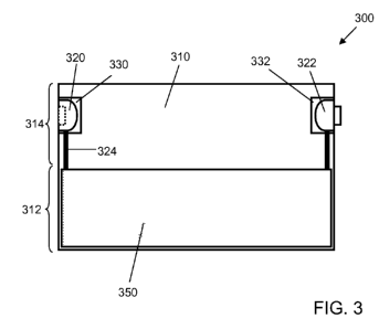
[0057] FIG. 3 is a schematic top view and FIG. 4 is a schematic cross-
sectional
view of a photovoltaic roofing element according to one embodiment of the
invention.
Photovoltaic roofing element 300 includes a flexible roofing substrate 310
(here, an
asphalt shingle) having a exposure zone 312 (i.e., the part of the shingle
that will be
exposed when installed on a roof) and a headlap zone 314 (the part that will
be
covered by an overlying course of shingles). A photovoltaic element 350 is
disposed
on the flexible roofing substrate in the exposure zone. The photovoltaic
element
further includes two electrical connectors (here, mating electrical
connectors) 320 and
322, which are operatively coupled to the photovoltaic element 350, in this
embodiment through wires 324. The mating electrical connectors in this
embodiment
mate in a male/female fashion. The flexible roofing substrate has recesses 330
and
13
WO 2010/068677 PCT/US2009/067352
332 formed therein, which are adapted to at least partially receive the mating
electrical connectors 320 and 322.
[0058] In the embodiment of FIGS. 3 and 4 the electrical connectors are
disposed
entirely within the recesses. In other embodiments, the electrical connectors
can be
only partially disposed within the recesses; that is, some portion of an
electrical
connector can in some circumstances protrude from the recess. The electrical
connectors can be affixed into the recesses, or alternatively can be merely
held within
them.
[0059] In cases where no recess is provided for the wires connecting the
photovoltaic element to the mating electrical connector, they are desirably
relatively
flat in cross-sectional shape, so as not to cause a significant bump in an
overlying
roofing element. In certain other embodiments, the wires are disposed within
the
flexible roofing substrate itself.
[0060] The recess can be formed in a variety of surfaces of the flexible
roofing
substrate. For example, as shown in FIGS. 3 and 4, the recess can be formed in
a top
surface of the flexible roofing substrate. As shown in FIG. 4, the recess does
not go
through the thickness of the entire asphalt shingle.
[0061] Another embodiment is shown in cross-sectional view in FIG. 5. In this
photovoltaic roofing element 500, the top view is similar to that shown in
FIG. 3, but
the recess is formed in the side of the flexible roofing substrate 510, and
the recess
530 goes all the way through the flexible roofing substrate. This
configuration can be
advantaged in that it would prevent pooling of any water that is blown-back up
underneath the overlying roofing elements. In other embodiments, a sealing
film can
be applied to the flexible roofing substrate in the neighborhood of the recess
(e.g., on
its top surface, on its bottom surface, or both), so as to provide a water-
resistant seal.
[0062] A recess can be formed through less than all layers of a multilayer
asphalt
shingle (or other flexible roofing substrate). For example, the recess can be
formed as
a hole or cutout in at least one, but not all the layers of a multilayer
asphalt shingle.
[0063] Another embodiment is shown in top schematic view in FIG. 6. In
photovoltaic roofing element 600, the flexible roofing substrate 610 has a
recess 630
14
WO 2010/068677 PCT/US2009/067352
which is adapted to at least partially receive not only the mating electrical
connectors
620 and 622, but also the wires 624 that operatively connect them to the
photovoltaic
element 650. In this embodiment, the wires can be relatively thick, but still
not cause
distortion of overlying layers of flexible roofing materials. In other
embodiments,
the recess can be shaped to at least partially receive other electrical
connectors, such
as bypass diodes and junction boxes.
[0064] Another embodiment is shown in top schematic view in FIG. 7. In this
embodiment, the recess 730 is formed in a bottom surface of the flexible
roofing
substrate. The mating electrical connectors 720, 722 and the wires 724 are
disposed
on the top surface of the flexible roofing substrate 710. In this embodiment,
the
recess is of a shape to at least partially receive the electrical connectors.
However,
when installed, the mating electrical connectors of this photovoltaic roofing
element
700 will not be disposed within the recess 730. Rather, as will be described
in more
detail with reference to FIG. 18, in use the recess 730 of this photovoltaic
roofing
element can at least partially receive the electrical connectors of a similar,
underlying
photovoltaic roofing element, and the electrical connectors 720, 722 of this
photovoltaic roofing element 730 can be at least partially received by the
recess of a
similar, overlying photovoltaic roofing element.
[0065] In other embodiments, as shown in top view in FIG. 8, and cross-
sectional
view in FIG. 9, the electrical connector is partially received within the
recess, yet
protrudes partially from the top face of the photovoltaic roofing element. In
photovoltaic element 800, the photovoltaic elements 850 and their associated
series
interconnection wiring 824, bypass diode 826 and return electrical path wiring
828
mating electrical connectors 820, 822 are contained within a laminate or
encapsulated
structure 870, from which the mating electrical connectors protrude. The
return
electrical path wiring can allow for the mating electrical connectors to not
only
interconnect the photovoltaic elements of adjacent photovoltaic roofing
elements in
series, but also allow provide the return path for built-up power to the
larger electrical
system. The return path wiring can be as described in U.S. Provisional Patent
Application serial no. 61/040,376, which is hereby incorporated herein by
reference in
its entirety. In the embodiment of FIG. 9, the mating electrical connectors
protrude
from both the bottom and top faces of the laminate structure. In other
embodiments,
WO 2010/068677 PCT/US2009/067352
the mating electrical connectors protrude only from the top surface, or only
from the
bottom surface of the laminate or encapsulated structure. In the embodiment of
FIG.
9, the laminate structure 870 is disposed on a flexible roofing substrate 810.
The
flexible roofing substrate 810 has a recess 830 formed therein to receive the
mating
electrical connector 820; as well as a second recess formed therein (not shown
in the
cross-sectional view of FIG. 9) to receive the mating electrical connector
822. In
certain embodiments, for example when the electrical connectors protrude
significantly from the top face of the laminate or encapsulated structure, the
flexible
roofing substrate 810 can have a recess formed in its bottom surface, as
described
above with reference to FIG. 7 and below with reference to FIG. 18.
[0066] In certain embodiments, the flexible roofing substrate itself is made
from a
plurality of layers of material. In such embodiments, the various layers can
be cut or
notched differently to form the recess. For example, in the embodiment of FIG.
10,
the flexible roofing substrate 1010 includes two layers of material (e.g.,
asphalt-
impregnated fiberglass web, as used in conventional roofing shingles). In the
first
layer 1012, a notch 1034 (shown as a discontinuity in this cross-sectional
view) is cut
to receive the electrical connector 1020. The second layer 1014 underlies the
first
layer and the electrical connector. The overall effect of the notch 1034 and
the
underlying layer 1014 is that of a recess formed in the top surface of the
flexible
roofing substrate, as described above.
[0067] In certain embodiments of the invention, the wiring that operatively
connects the mating electrical connectors to the photovoltaic element can have
sufficient slack to allow the connectors to be lifted away from the flexible
roofing
substrate for easy interconnection with the mating electrical connector of
another
photovoltaic roofing element, or into a larger electrical system. In some such
embodiments, the slack wire can be received by a recess in a flexible roofing
substrate
(i.e., either in the flexible roofing substrate of its own photovoltaic
roofing element, or
the flexible roofing substrate of an overlying flexible roofing substrate, as
described
above with reference to FIG. 7 and below with reference to FIG. 18. An example
of
this is shown in FIG. 6, in which the slack in wiring 624 is received by
recess 630.
[0068] FIG. 11 is a top perspective schematic view, and FIG. 12 is a cross-
sectional schematic view of a photovoltaic roofing element 1100 according to
another
16
WO 2010/068677 PCT/US2009/067352
embodiment of the invention. In this embodiment, the laminate or encapsulate
structure 1170 has a reduced volume of encapsulant or laminating materials in
the
headlap zone of the structure (i.e., there is no encapsulant or laminating
material in
most of the headlap zone 1118 of the photovoltaic roofing element 1100). Such
an
arrangement can make more efficient use of costly encapsulant or laminating
materials by encapsulating or laminating primarily the parts of the structure
that
include electrical wiring or photovoltaic materials, and generally avoiding
the use of
encapsulant or laminate materials in portions of the structure that will not
be exposed
to the weather. In other embodiments, wires or cables can connect the mating
electrical connectors to a laminated or encapsulated photovoltaic element
[0069] In the photovoltaic roofing element of FIGS. 11 and 12, the laminate or
encapsulate structure 1170 includes photovoltaic elements 1150, bypass diode
1126,
return path wiring 1128 and wiring 1124, as well as mating electrical
connectors
1120, 1122. The mating electrical connectors protrude both and above and below
the
laminate or encapsulate structure. The flexible roofing substrate 1110
includes a first
layer 1112 which has a notch 1134 cut therein to receive the mating electrical
connector 1120, and a second layer 1114 which underlies the first layer. In
certain
embodiments, the first layer merely has a recess formed therein, instead of a
notch
formed through its entire thickness. The second layer does not have notches in
the
vicinity of the mating electrical connectors, thus providing closure and a
water and
weather proofing of the photovoltaic roofing element. The photovoltaic roofing
element 1100 also includes a top layer of flexible roofing material 1180
(shown in
dotted outline in FIG. 11) in the headlap zone, which has a notch formed
therein to
accommodate the mating electrical connectors. In this embodiment, the mating
electrical connectors protrude only slightly above the top layer of flexible
roofing
material, and when installed has little effect on the aesthetics of an
overlying
photovoltaic roofing element. In other embodiments, the second layer of the
flexible
roofing substrate has a hole cut therein, to form a recess formed in the
bottom surface
of the flexible roofing substrate, as described above with reference to FIG. 7
and
below with reference to FIG. 18.
[0070] FIGS. 13, 14 and 15 are top perspective schematic views of a
photovoltaic
roofing element and its components according to another embodiment of the
17
WO 2010/068677 PCT/US2009/067352
invention. FIG. 13 shows a flexible roofing substrate 1310, which has a first
layer
1312, a second layer 1313 and a third layer 1314. The first and second layers
are only
in the headlap zone 1318, and have corners cut out to provide a recess 1330
for
electrical connectors. The third layer forms a support base for the entire
photovoltaic
roofing element, and can have a photovoltaic receptor zone 1382 that is
adapted to
receive a photovoltaic element, for example as described in U.S. Provisional
Patent
Application serial no. 61/043,707 filed April 9, 2008, in U.S. Provisional
Patent
Application serial no. 61/014,902 filed December 19, 2007 and in U.S. Patent
Application Publication no. 2009/0159118, each of which is hereby incorporated
herein by reference in its entirety. As described above, the flexible roofing
substrate
1310 can be formed from, for example, asphalt-impregnated fiberglass web
materials,
as are common in the roofing arts. FIG. 14 shows a photovoltaic element 1350
in a
laminate structure 1370. Junction boxes 1352 interconnect the photovoltaic
element
to mating electrical connectors 1320. The junction box can also, in some
embodiments, include a bypass diode.
[0071] FIG. 15 shows a photovoltaic roofing element 1300 assembled from the
laminate structure of FIG. 14 and the flexible roofing substrate of FIG. 13.
In one
embodiment the assembly is pre-assembled in a manufacturing environment. In
another embodiment, the assembly is assembled in the field, the flexible
roofing
substrate having a receptor zone as described in U.S. Provisional Patent
Application
serial no. 61/043,707 filed April 9, 2008, in U.S. Provisional Patent
Application serial
no. 61/014,902 filed December 19, 2007 and in U.S. Patent Application
Publication
no. 2009/0159118, each of which is hereby incorporated herein by reference in
its
entirety.
[0072] Asphalt shingle constructions are known in the shingle art and can be
used
as the flexible roofing substrates in various aspects of the present
invention.
Alternatively, other flexible base materials such as elastomeric membrane,
polyvinylchloride membrane, thermoplastic polyolefin membrane or other
flexible
polymeric materials may be used.
[0073] Another aspect of the invention is shown in top schematic view in FIG.
16.
Photovoltaic roofing system 1690 includes a first photovoltaic roofing element
1600,
which comprises a flexible roofing substrate, a photovoltaic element disposed
on the
18
WO 2010/068677 PCT/US2009/067352
flexible roofing substrate, and an electrical connector operatively coupled to
the
photovoltaic element, as described above. Photovoltaic roofing system 1690
further
comprises a second photovoltaic roofing element 1605, shown in dotted outline,
which comprises a flexible roofing substrate, a photovoltaic element disposed
on the
flexible roofing substrate, and an electrical connector operatively coupled to
the
photovoltaic element, as described above. The second photovoltaic roofing
element
1605 is disposed so as to cover the electrical connector of the first
photovoltaic
roofing element. In certain embodiments, the electrical connectors of the
first
photovoltaic roofing element are at least partially disposed within a recess
formed in
the flexible roofing substrate of the first photovoltaic roofing element
(e.g., in a top or
along a side thereof); within a recess formed in the flexible roofing
substrate of the
second photovoltaic roofing element (e.g., in a bottom surface thereof); or
within a
recess formed in the flexible roofing substrate of the first photovoltaic
roofing
element and within a recess formed in the flexible roofing substrate of the
second
photovoltaic roofing element. The photovoltaic roofing system can, for
example, be
disposed on a roof deck.
[0074] For example, in certain embodiments, as shown in side cross-sectional
view in FIG. 17, the flexible roofing substrate of the first photovoltaic
roofing
element 1700 has a recess 1730 formed in its top surface or along a side, in
which the
electrical connector of the first photovoltaic roofing element is at least
partially
disposed. Such a photovoltaic roofing element is described, for example, with
reference to FIGS. 3 and 4, above. In FIG. 17, the electrical connector 1720
of first
photovoltaic roofing element 1700 is covered by second photovoltaic roofing
element
1705 (shown in dotted outline). As the person of skill in the art will
understand, the
recesses (e.g., cutouts or notches) can advantageously be disposed so that,
when
installed, they are aligned in a way to minimize the formation of water
pathways
through the flexible roofing substrates.
[0075] Another aspect of the invention is a photovoltaic roofing system
comprising: a first photovoltaic roofing element, the first photovoltaic
roofing
element comprising a flexible roofing substrate, a photovoltaic element
disposed on
the flexible roofing substrate, and an electrical connector operatively
coupled to the
photovoltaic element; and a second photovoltaic roofing element disposed
adjacent
19
WO 2010/068677 PCT/US2009/067352
the first photovoltaic roofing element, the second photovoltaic roofing
element
comprising: a flexible roofing substrate having a recess formed therein, the
electrical
connector of the first photovoltaic roofing element being at least partially
disposed in
the recess, a photovoltaic element disposed on the flexible roofing substrate,
and an
electrical connector operatively coupled to the photovoltaic element. For
example, as
shown in side cross-sectional view in FIG. 18, the flexible roofing substrate
of the
second photovoltaic roofing element has a recess formed in its bottom surface,
in
which the electrical connector of the first photovoltaic roofing element is at
least
partially disposed. Such a photovoltaic roofing element is described, for
example,
with reference to FIG. 7, above. In FIG. 18, the electrical connector 1820 of
the first
photovoltaic roofing element 1800 is disposed in a recess 1830 formed in the
bottom
side of the flexible roofing substrate of the second photovoltaic roofing
element 1805
(shown in dotted outline). While not shown in this cross-sectional view (due
to the
lateral offset between the photovoltaic roofing elements as shown in FIG. 16),
the
second photovoltaic roofing element can have a electrical connector, and the
first
photovoltaic roofing element can have a recess formed in the bottom surface of
its
flexible roofing substrate. For example, the first and second photovoltaic
roofing
elements can be the same. As the person of skill in the art will appreciate,
the
position of the recess will depend on the positions of the electrical
connectors as well
as the intended configuration (i.e., lateral offset between courses, degree of
overlap
between courses) of the photovoltaic roofing elements in a larger photovoltaic
roofing
system. For example, if a photovoltaic roofing element has its electrical
connectors at
a higher position (i.e., closer to the roof ridge end of the photovoltaic
roofing
element), a recess on the bottom surface would be at a different location than
for
embodiments having electrical connectors at a lower position. For photovoltaic
roofing elements to be applied with a consistent lateral offset during
installation, a
recess can be appropriately located so as to be able to receive the electrical
connectors
of an underlying course. For photovoltaic roofing elements that are to be
applied with
an alternating offset, such as in a racked-type installation, it may be that
they include
two recesses, one toward a left end and one toward a right end so that the
same
photovoltaic roofing elements may be used as courses are built up on the roof
with
alternating left and right offsets in the installation pattern.
WO 2010/068677 PCT/US2009/067352
[0076] FIG. 19 shows a photovoltaic roofing system comprising an array of
photovoltaic roofing elements as described herein. The photovoltaic roofing
elements
are disposed in a laterally-offset fashion as sequential courses are applied
on a roof
deck (roof deck not shown). As the person of skill in the art will understand,
the
number of courses and the number of photovoltaic roofing elements per course
will
depend on the size of the roof area to be covered, and may include more or
fewer
courses than three, and more or fewer photovoltaic roofing elements per course
than
three. In FIG. 19, the upper two courses are shown in dotted outline, so as to
show
the locations of the structural details of the underlying courses, including
the locations
of the electrical connectors and interconnections between photovoltaic roofing
elements. As described in detail above, the electrical connectors can be
disposed
within recesses formed in the photovoltaic roofing elements of which they are
a part,
within recess formed in overlying photovoltaic roofing elements, or
(advantageously
for relatively thick electrical connectors) both.
[0077] FIG. 20 shows a photovoltaic roofing system similar to that of FIG. 19,
in
which the photovoltaic roofing elements are disposed in a racked
configuration, in
which the laterally offset disposition as sequential courses are applied on a
roof deck
(roof deck not shown) alternates from left to right relative to the underlying
course
moving up the roof.
[0078] One aspect of the invention is a photovoltaic roofing element including
a
flexible roofing substrate, the flexible roofing substrate including a base of
flexible
roofing material having a top surface, the top surface having a headlap zone
and an
exposure zone, and one or more layers of shim material disposed on the top
surface of
the base in the headlap zone; a photovoltaic element disposed on the top
surface of the
base; and an electrical connector operatively connected to the photovoltaic
element
and disposed on the top surface of the base, wherein the one or more layers of
shim
material have a total thickness at least about as great as the thickness of
the electrical
connector. That is, the combined thicknesses of the one or more layers of shim
material is at least about as great as the thickness of the electrical
connector.
[0079] For example, the total thickness of the one or more layers of shim
material
can be about equal to (e.g., within 20% of, or even within 10% of) the
thickness of
the electrical connector. As used herein, the headlap zone is the area that is
covered
21
WO 2010/068677 PCT/US2009/067352
by overlying courses of roofing elements when installed; and the exposure zone
is the
area that is not covered by overlying courses of roofing elements when
installed.
[0080] In one embodiment, the one or more layers of shim material have a stair-
step configuration, for example with the region of greatest thickness disposed
adjacent
the electrical connector. In such an embodiment, the stair-step can provide a
gradual
slope to an overlying flexible roofing element.
[0081] In one embodiment, the one or more layers of shim material have a notch
or recess formed therein, in which the connector is positioned.
[0082] Another aspect of the invention is a photovoltaic roofing element
including
a flexible roofing substrate, the flexible roofing substrate including a base
of flexible
roofing material having a top surface and a bottom surface, the top surface
having a
headlap zone and an exposure zone; and one or more layers of shim material
disposed
on the bottom surface of the flexible roofing substrate; a photovoltaic
element
disposed on the top surface of the base; and an electrical connector
operatively
connected to the photovoltaic element and disposed on the top surface of the
base,
wherein the one or more layers of flexible roofing material have a total
thickness at
least about as great as the thickness of the electrical connector.
[0083] For example, the total thickness of the one or more layers of flexible
roofing material can be about equal to (e.g., within 20% of, or even within
10% of )
the thickness of the electrical connector.
[0084] In certain embodiments, the photovoltaic roofing element includes a
plurality of electrical connectors, for example, mating electrical connectors,
junction
boxes, bypass diodes, wiring and/or cabling. Any or all of the electrical
connectors
can be protected by the shim layers as described herein.
[0085] In one embodiment, the one or more layers of shim material are
positioned
so that, when installed, the electrical connector of an underlying
photovoltaic roofing
element is disposed adjacent the one or more layers. In some embodiments, a
sealing
layer for containment and waterproofing of the connector element is provided.
22
WO 2010/068677 PCT/US2009/067352
[0086] In one embodiment, the one or more layers of flexible roofing material
have a stair-step configuration, for example with the region of greatest
thickness
positioned so that, when installed, the electrical connector of an underlying
photovoltaic roofing element is disposed adjacent the region of greatest
thickness.
[0087] In one embodiment, the one or more layers of flexible roofing material
have a notch or recess formed therein, positioned so that, when installed, the
electrical
connector of an underlying photovoltaic roofing element is disposed therein.
[0088] Another aspect of the invention is photovoltaic roofing system
comprising
a plurality of photovoltaic roofing elements as described herein electrically
interconnected and disposed on a roof.
[0089] One embodiment of the invention is shown in side schematic cross-
sectional view in FIG. 21, and in top schematic view in FIG. 22. A
photovoltaic
roofing element 2100 includes flexible roofing substrate 2110, which in turn
includes
a base of flexible roofing material 2120, which has top surface 2122 having a
headlap
zone 2124 and an exposure zone 2126, and a bottom surface 2128; and a layer of
shim
material 2130 disposed on the top surface of the base in the headlap zone. The
photovoltaic roofing element 2100 also includes a photovoltaic element 2140
disposed on the top surface of the base in the exposure zone, and an
electrical
connector 2150 disposed on the base and operatively coupled (e.g., through
cable
2152) to the photovoltaic roofing element. The layer of shim material 2130 has
a total
thickness at least about as great as the thickness of the electrical connector
2150. For
example, in the embodiment of FIGS. 21 and 22, the thickness of the layer of
shim
material is about equal to the thickness of the electrical connector.
[0090] In the embodiment of FIGS. 21 and 22, the electrical connector is shown
as sitting entirely on top of the base of flexible roofing material. In other
embodiments, the electrical connector can be partially embedded in the roofing
material, or be partially disposed in a recess pre-formed therein.
[0091] The cable 2152 can be round in cross section, or in certain embodiments
can have a flat cross-section (e.g., a relatively flat ribbon of metal clad in
a plastic
coating). The person of skill in the art can select a flat cable having
sufficient
electrical properties for the transmission of electric power through the
photovoltaic
23
WO 2010/068677 PCT/US2009/067352
system. A flat cable can be folded over so as to lie flat, and can be easily
bent to
change direction. Advantageously, the flat cable can lie between photovoltaic
roofing
elements without causing a protrusion.
[0092] FIG. 23 is a cross-sectional schematic view of a photovoltaic roofing
system 2160, which comprises a plurality of photovoltaic roofing elements 2100
as
described above with reference to FIGS. 21 and 22. Overlying courses of
photovoltaic roofing elements lay flat on top of the shim material, so that
the
electrical connector itself does not protrude, and is therefore more protected
from
damage. In cases where the shim material is flexible (e.g., when it is made
from
flexible roofing material such as that used for the base), the headlap portion
of the can
flex to contact the roof (not shown). The photovoltaic roofing system can be
disposed
on a roof deck and interconnected with an electrical system to form a
photovoltaic
roofing system.
[0093] Another embodiment of the invention is shown in side schematic cross-
sectional view in FIG. 24, and in top schematic view in FIG. 25. A
photovoltaic
roofing element 2400 includes flexible roofing substrate 2410, which in turn
includes
a base of flexible roofing material 2420, which has top surface 2422 having a
headlap
zone 2424 and an exposure zone 2426, and a bottom surface 2428; and a layer of
shim
material 2430 disposed on the bottom surface of the base. The photovoltaic
roofing
element 2400 also includes a photovoltaic element 2440 disposed on the top
surface
of the base, and an electrical connector 2450 disposed on the base and
operatively
coupled (e.g., through cable 2452) to the photovoltaic roofing element. The
layer of
shim material 2430 (position shown in dashed line in FIG. 25) has a total
thickness at
least about as great as the thickness of the electrical connector 2450. For
example, in
the embodiment of FIGS. 24 and 25, the thickness of the layer of shim material
is
about equal to the thickness of the electrical connector. Notably, in the
embodiments
of FIGS. 24-25, the layer of shim material is positioned so that, when
installed, the
electrical connector of an underlying photovoltaic roofing element (shown in
dotted
lines) is disposed adjacent the layer of shim material.
[0094] FIG. 26 is a cross-sectional schematic view of a photovoltaic roofing
system 2460, which comprises a plurality of photovoltaic roofing elements 2400
as
described above with reference to FIGS. 24 and 25. Overlying courses of
24
WO 2010/068677 PCT/US2009/067352
photovoltaic roofing elements lay on top of the shim material, with any bump
or
protrusion formed by the shim material, so that the electrical connector
itself does not
protrude, and is therefore more protected from damage.
[0095] The shim material can have a shape that provides a recess (e.g., notch
or
cut-away) into which the connector can fit. For example, as shown in top
schematic
view in FIG. 27, a photovoltaic roofing element 2700 includes flexible roofing
substrate, which in turn includes a base of flexible roofing material 2720,
which has
top surface having a headlap zone 2724 and an exposure zone 2726, and a bottom
surface (not shown in this view); and a layer of shim material 2730 disposed
on the
top surface of the base in the headlap zone. The photovoltaic roofing element
2700
also includes a photovoltaic element 2740 disposed on the top surface of the
base in
the exposure zone, and an electrical connector 2750 disposed on the base and
operatively coupled to the photovoltaic roofing element. The layer of shim
material
2730 has a total thickness at least about as great as the thickness of the
electrical
connector 2750. In the embodiment of FIG. 27, the shim material has cutaways
2732
in which the electrical connectors 2750 are disposed.
[0096] The shim material can be any of a variety of materials. For example, in
order to provide for ease of manufacturing in conventional roofing shingle
production
processes, the shim materials can be layers of asphalt shingle material. In
other
embodiments, the shim material can be plastic. The shim material can, for
example,
include recycled content, such as recycled plastic, recycled asphalt, or other
recycled
roofing materials. Layers of different shim materials can be mixed in a single
photovoltaic roofing element according to one embodiment of the invention.
[0097] In one embodiment, the one or more layers of shim material have a
slanted
profile that provides a relatively gradual slope to an overlying roofing
element. For
example, as shown in side schematic cross-sectional view in FIG. 28, a layer
of shim
material 2830 disposed on top surface 2822 of the base of roofing material
2820 is
slanted at its end furthest from the down-roof edge 2825 of the base of
roofing
material, so that an overlying roofing element (shown in dotted outline) can
more
gradually slope over the electrical connector 2850. Similarly, as shown in
side
schematic cross-sectional view in FIG. 29, a layer of shim material 2930
disposed on
the bottom surface 2928 of a base of roofing material 2920 can be slanted at
its end
WO 2010/068677 PCT/US2009/067352
furthest from the down-roof edge 2925 of the base of roofing material, so that
the base
of roofing material can more gradually slope over the electrical connector
2951 of an
underlying photovoltaic roofing element (shown in dotted line).
[0098] In another embodiment, the one or more layers of shim material have a
stair-step profile. The stair-step profile can provide a relatively gradual
slope as
described above with reference FIGS. 28 and 29, and can be made more simply,
for
example, using methods used conventionally in the production of roofing
products. In
one embodiment, shown in side schematic side view in FIG. 30 and in schematic
top
view in FIG. 31, photovoltaic roofing element 3000 includes flexible roofing
substrate
3010, which in turn includes a base of flexible roofing material 3020, which
has top
surface 3022 having a headlap zone 3024 and an exposure zone 3026, and a
bottom
surface 3028. Base 3020 in this embodiment is made of two layers of roofing
material (e.g., reinforced asphalt), a first layer 3020a that forms the bottom
of the
entire photovoltaic roofing element, and a second layer 3020b that is formed
only in
the headlap zone. The flexible roofing substrate 3010 further includes a stack
3030 of
three layers of shim material 3032, 3034 and 3036 disposed in a stair-step
configuration on the top surface of the base in the headlap zone. The layers
3032,
3034 and 3036 have corners cut out to form recesses for electrical connectors.
The
photovoltaic roofing element 3000 also includes a photovoltaic element 3040
disposed on the top surface of the base, and an electrical connector 3050
disposed on
the base (here, on the second layer 3020b) and operatively coupled to the
photovoltaic
roofing element. The stack of shim material 3030 has a total thickness at
least about
as great as the thickness of the electrical connector 3050. For example, in
the
embodiment of FIGS. 30 and 31, the total thickness of the layers of shim
material is
about equal to the thickness of the electrical connector. The electrical
connector is
disposed in a cutout region of the layers of shim material. In such
embodiments, the
flexible roofing substrate and shim materials can be formed from reinforced
bituminous materials, like conventional (fiber) glass-reinforced or polyester
or
polyester/fiber glass composite asphalt materials.
[0099] In one embodiment, for example, a photovoltaic roofing element as
described above with reference to FIGS. 30 and 31 has an overall height (i.e.,
distance
down the roof from the top of the headlap zone 3024 to the bottom of the
exposure
26
WO 2010/068677 PCT/US2009/067352
zone 3026) of about 18". The first layer 3020a of the base has a height of
18", and
the second layer 3020b has a height of 9.625". The three shim layers 3032,
3034,
3036 have heights of 7", 5" and 3", respectively.
[0100] Similarly, as shown in the photovoltaic roofing element 3200 in FIG.
32,
layers of shim material 3232, 3234, 3236 can be disposed in a stair-step
fashion on the
bottom surface 3228 of the base 3220 to allow it to more easily fit over a
connector on
an underlying course of photovoltaic elements, as described with reference to
FIGS.
24-26 and 28.
[0101] In one embodiment the assembly is pre-assembled in a manufacturing
environment. In another embodiment, the assembly is assembled in the field,
the
shingle support having a receptor zone as described in U.S. Provisional Patent
Application serial no. 61/043,707 filed April 9, 2008, in U.S. Provisional
Patent
Application serial no. 61/014,902 filed December 19, 2007 and in U.S. Patent
Application Publication no. 2009/0159118, the entirety of each of which is
incorporated herein by reference.
[0102] Asphalt shingle constructions are known in the shingle art and can be
used
for the base material. Alternatively, other flexible base materials such as
elastomeric
membrane, polyvinylchloride membrane, thermoplastic polyolefin membrane or
other
flexible polymeric materials may be used. The shim materials can be the same
as the
flexible base materials, or may be different. When the shim materials are the
same as
the flexible base materials, the roofing substrates can be formed using multi-
layer
shingle production processes familiar to the person of skill in the art.
[0103] Another aspect of the invention is a photovoltaic system including a
plurality of photovoltaic roofing elements as described above, electrically
interconnected. The photovoltaic system (e.g., a photovoltaic roofing system)
can be
interconnected with an inverter to allow photovoltaically-generated electrical
power
to be used on-site, stored in a battery, or introduced to an electrical grid.
[0104] In certain embodiments of the invention a plurality of photovoltaic
roofing
elements are disposed on a roof deck and electrically interconnected to form a
photovoltaic roofing system. There can be one or more layers of material (e.g.
underlayment), between the roof deck and the photovoltaic laminates/roofing
27
WO 2010/068677 PCT/US2009/067352
elements. The roof can also include one or more standard roofing elements, for
example to provide weather protection at the edges of the roof, or in areas
not suitable
for photovoltaic power generation. In some embodiments, non-photovoltaically-
active roofing elements are complementary in appearance or visual aesthetic to
the
photovoltaic roofing elements.
[0105] Any cabling interconnecting the photovoltaic roofing elements of the
invention in a photovoltaic roofing system can, for example, be long and
flexible
enough to account for natural movement of a roof deck, for example due to
heat,
moisture and/or natural expansion/contraction.
[0106] It will be understood that power generated by the photovoltaic roofing
systems described herein may be used to power the building itself or may be
directed
elsewhere on an electrical grid, as desired. Electrical systems for handling
the
photovoltaically-generated power are described, for example, in 11/743,073,
which is
hereby incorporated herein by reference in its entirety. Photovoltaic elements
suitable
for use in the present invention are described in, for example, in U.S. Patent
Application serial no. 12/266,409, which is hereby incorporated herein by
reference in
its entirety.
[0107] Another aspect of the invention is a method for installing a
photovoltaic
roofing system comprising disposing on a roof and electrically interconnecting
a
plurality of photovoltaic roofing elements as described herein. The disposal
on the
roof and electrical interconnections can be performed in any desirable order.
In
certain embodiments, the photovoltaic roofing elements themselves can be
assembled
on the roof, for example in conjunction with electrically interconnecting
them, as
described above with reference U.S. Provisional Patent Application serial no.
61/043,707 filed April 9, 2008, U.S. Provisional Patent Application serial no.
61/014,902 filed December 19, 2007 and U.S. Patent Application Publication no.
2009/0159118, the entirety of each of which is incorporated herein by
reference.
[0108] Another aspect of the invention is a roof comprising a roof deck and a
photovoltaic roofing system as described herein disposed on the roof deck. The
photovoltaic roofing elements described herein can be utilized with many
different
28
WO 2010/068677 PCT/US2009/067352
building structures, including residential, commercial and industrial building
structures.
[0109] Another aspect of the invention is a kit for the installation of a
photovoltaic roofing system, the kit comprising a plurality of photovoltaic
roofing
elements as described herein.
[0110] Further, the foregoing description of embodiments of the present
invention
has been presented for the purposes of illustration and description. It is not
intended to
be exhaustive or to limit the invention to the precise forms disclosed. As the
person
of skill in the art will recognize, many modifications and variations are
possible in
light of the above teaching. It will be apparent to those skilled in the art
that various
modifications and variations can be made to the present invention without
departing
from the scope of the invention. Thus, it is intended that the present
invention cover
the modifications and variations of this invention provided they come within
the
scope of the claims and their equivalents.
29