Note: Descriptions are shown in the official language in which they were submitted.
CA 02756125 2014-02-24
54106-967
LOW-PROFILE ELECTRONIC CIRCUIT BREAKERS, BREAKER TRIPPING
MECHANISMS, AND SYSTEMS AND METHODS OF USING SAME
RELATED APPLICATIONS
[001] This application claims priority to U.S. Provisional
Application Serial Number 61/162,731 entitled "ELECTRONIC
CIRCUIT BREAKER WITH TWIN OR DUPLEX MECHANICAL POLES'
filed on March 24, 2009, U.S. Provisional Application
Serial Number 61/162,417 entitled "CIRCUIT BREAKER ARC
CHAMBER DESIGN THAT FACILITATES INTERRUPTIONS" filed on
March 23, 2009, and U.S. Provisional Application Serial
Number 61/302,283 entitled "CIRCUIT BREAKER WITH ENHANCED
INTERRUPTION CAPABILITY" filed on February 08, 2010.
FIELD OF THE INVENTION
[002] The present invention relates generally to circuit
breakers for interrupting current from an electrical
power supply, and more particularly to electronic circuit
breakers including two internal electrical branches and
tripping mechanisms for circuit breakers.
BACKGROUND OF THE INVENTION
[003] Electronic circuit breakers are used in certain
electrical systems for protecting an electrical circuit
(hereinafter "protected circuit") coupled to an
electrical power supply. For example, one type of
electrical circuit breaker is a ground fault circuit
interrupter (GFCI). GFCIs are utilized in electrical
systems to prevent electrical shock hazards, and are
typically included in electrical circuits adjacent to
water, such as in residential bathrooms or kitchens.
Another type of electronic circuit breaker is an arc
fault circuit interrupter (AFCI). AFCIs interrupt power
to an electrical circuit when an arcing situation is
1
C. 02756,25 2011 09 2i
W02010/111210
PCT/US2010/028219
detected within the circuit. GFCIs and AFCIs may also
provide persistent over current and short circuit
protection, and provide for hand circuit breaker tripping
as well. GFCI's and AFCI's are within the class of
"electronic circuit breakers" and include an internal
printed circuit board, which together with one or more
onboard sensors may detect changes in an electrical
condition within the protected circuit and trip a
tripping mechanism of the electronic circuit breaker.
[0(141 Because such GFCIs and AFCIs include numerous
electronic components such as printed circuit boards,
sensors, and electromagnets, as well as mechanical
components such as contact arms, electrical contacts,
cradles, springs, armatures, magnets and bimetal
elements to accomplish the tripping function, and
terminals, lugs, lug screws and internal wiring for
connection to the protected circuit and circuit breaker
panelboard, packaging of such electronic circuit
breakers within a small space envelope has not been
possible, particularly in the case of duplex electronic
circuit breakers. Accordingly, in the case of
conventional duplex electronic circuit breakers, which
include two internal electrical branches, such breakers
have been configured to take up two standard circuit
breaker locations within the panelboard. As such,
conventional duplex electronic circuit breakers to date
have exhibited either an overall width of 1% inches
thereby occupying two %-inch standard panelboard
spaces, or an overall width of 2 inches, thereby
occupying two 1-inch standard panelboard spaces.
[005] Accordingly, there is a long-felt and unmet need for
an electronic circuit breaker having two electrical
branches which exhibits a lower profile (i.e., a lower
overall transverse width).
2
c.mw25m0,2,
WO 2010/111210
PCT/US2010/028219
SUMMARY OF THE INVENTION
[006] In a first aspect, an electronic circuit breaker
including two electrical branches is provided. The
electronic circuit breaker includes a housing containing
a first branch and a second branch and, the housing
having a maximum transverse width (Wt); a first load
terminal coupled to the first branch; a second load
terminal coupled to the second branch; and an electronic
processing circuit within the housing adapted to monitor
an electrical condition of one or more of the first
branch and the second branch, wherein the maximum
transverse width (Wt) of the housing is limited so as to
occupy only a single standard breaker panelboard
location.
[007] In another aspect, an electrical panelboard system
is provided. The electrical panelboard system includes a
panelboard including a plurality of standard circuit
breaker mounting locations; and an electronic circuit
breaker including a first branch and a second branch, the
electronic circuit breaker occupying a single standard
mounting location on the panelboard.
[008] According to another aspect, a method of installing
an electronic circuit breaker is provided. The method
includes providing a panelboard including a plurality of
standard circuit breaker mounting locations; and mounting
an electronic circuit breaker including a first branch
and a second branch on the panelboard such that the
electronic circuit breaker occupies a single standard
circuit breaker mounting location on the panelboard.
[009] In yet another aspect, a circuit breaker is
provided. The circuit breaker includes a housing
containing a moveable electrical contact; and a tripping
mechanism coupled to a moveable electrical contact, the
tripping mechanism including a tripping unit having a
magnet, a bimetal member extending alongside of the
magnet, and an armature pivotable on the magnet, the
3
CA 02756125 2016-05-26
54106-967
armature having an engagement portion engageable with the
bimetal member at a moveable end of the bimetal member.
[0010] In another aspect, a tripping unit of a circuit
breaker is provided. The tripping unit includes a magnet; a
bimetal member extending alongside of the magnet; and an
armature pivotable on the magnet, the armature having an
engagement portion engageable with the bimetal member at a
moveable end of the bimetal member.
[0010a] According to another aspect of the present invention,
there is provided an electronic circuit breaker, comprising: a
circuit breaker housing containing a first electrical branch
and a second electrical branch, the first and second branches
split from a power terminal and, the housing having a maximum
transverse width (Wt); a first load terminal coupled to the
first branch; a second load terminal coupled to the second
branch; an electronic processing circuit within the housing
adapted to monitor an electrical condition of one or more of
the first branch and the second branch; a first actuator and a
second actuator coupled to the electronic processing circuit,
the first and second actuators being disposed in a non-central
position within the circuit breaker housing to enable reduction
of the maximum transverse width (Wt), wherein the maximum
transverse width of the housing is limited so as to occupy only
a single standard breaker panelboard location, and wherein the
electronic circuit breaker is a two-pole electronic circuit
breaker.
[0010b] According to another aspect of the present invention,
there is provided an electrical panelboard system, comprising:
a panelboard including a plurality of standard circuit breaker
4
CA 02756125 2016-05-26
."54106-967
mounting locations; and an electronic circuit breaker including
a circuit breaker housing containing a first electrical branch
and a second electrical branch, the first and second branches
split from a power terminal, the electronic circuit breaker
occupying a single standard mounting location on the
panelboard, and wherein the electronic circuit breaker is a
two-pole electronic circuit breaker, and wherein the housing
has a maximum transverse width (Wt), and the electronic circuit
breaker further including a first load terminal coupled to the
first branch, a second load terminal coupled to the second
branch, an electronic processing circuit within the housing
adapted to monitor an electrical condition of one or more of
the first branch and the second branch, a first actuator and a
second actuator coupled to the electronic processing circuit,
the first and second actuators being disposed in a non-central
position within the circuit breaker housing to enable reduction
of the maximum transverse width (Wt).
[0010c] According to still another aspect of the present
invention, there is provided a method of installing an
electronic circuit breaker, comprising: providing a panelboard
including a plurality of standard circuit breaker mounting
locations; and mounting an electronic circuit breaker including
a circuit breaker housing containing a first electrical branch
and a second electrical branch, the first and second branches
split from a power terminal, on the panelboard such that the
electronic circuit breaker occupies a single standard circuit
breaker mounting location on the panelboard, and wherein the
electronic circuit breaker is a two-pole electronic circuit
breaker, and wherein the housing has a maximum transverse width
(Wt), and the electronic circuit breaker further including a
4a
CA 02756125 2016-05-26
54106-967
first load terminal coupled to the first branch, a second load
terminal coupled to the second branch, an electronic processing
circuit within the housing adapted to monitor an electrical
condition of one or more of the first branch and the second
branch, a first actuator and a second actuator coupled to the
electronic processing circuit, the first and second actuators
being disposed in a non-central position within the circuit
breaker housing to enable reduction of the maximum transverse
width (Wt).
[0011] Still other aspects, features, and advantages of the
present invention may be readily apparent from the following
detailed description by illustrating a number of exemplary
embodiments and implementations, including the best mode
contemplated for carrying out the present invention. The
present invention may also be capable of other and different
embodiments, and its several details may be modified in various
respects, all without departing from the scope of the present
invention. Accordingly, the drawings and descriptions are to be
regarded as illustrative in nature, and not as restrictive. The
invention is to cover all modifications, equivalents, and
alternatives falling within the scope of the invention.
BRIEF DESCRIPTION OF DRAWINGS
[0012] FIG. 1 is a perspective view of a low-profile
electronic circuit breaker including two branches according to
embodiments of the present invention.
[0013] FIG. 2 is a block diagram of an electrical system
including an electronic circuit breaker according to
embodiments of the present invention.
4b
CA 02756125 2016-05-26
.54106-967
[0014] FIG. 3 is a perspective view illustrating a portion
of the components of a first branch of an electronic circuit
breaker according to embodiments of the invention.
[0015] FIG. 4A is a side view illustrating a tripping
mechanism that may be employed in a circuit breaker, such
4c
C.027,6,2520.02,
WO 2010/111210
PCT/US2010/028219
as the electronic circuit breaker according to
embodiments of the invention.
[0016] FIG. 43 is a front view illustrating a portion
of a tripping unit of the tripping mechanism of FIG. 4A.
[0017] FIG. 4C is a side view illustrating the
tripping unit of FIG. 4B.
[0018] FIG. 4D is a front view illustrating an
armature of the tripping unit of FIG. 4A.
[0019] FIG. 4E is a side view illustrating the
armature of FIG. 4D.
[0020] FIG. 5A is a perspective view illustrating a
subassembly of a portion of the components of an
electronic circuit breaker according to embodiments of
the invention.
[0021] FIG. 53 is a perspective view illustrating a
second subassembly of a portion of the components of an
electronic circuit breaker according to embodiments of
the invention.
[0022] FIG. 6 is an exploded perspective view
illustrating various components of an electronic circuit
breaker according to embodiments of the invention.
[0023] FIGs. 7 and 8 are perspective views of opposite
sides of a subassembly of a portion of the components of
an electronic circuit breaker according to embodiments of
the invention.
[0024] FIGs. 9A and 9B are perspective views of the
load neutral terminals and other electrical harness
components of an electronic circuit breaker according to
embodiments of the invention.
[0025] FIG. 10 is a flowchart illustrating a method
according to embodiments of the invention.
[0026] FIG. 11A is a front view of a panel box
including a panelboard having an electronic circuit
breaker including two branches installed thereon
C. 02756,25 2011 09 2i
WO 2010/111210
PCT/US2010/028219
according to embodiments of the invention.
[0027] FIG. 113 is a perspective view of a panelboard
including an electronic circuit breaker mounted thereon
according to embodiments of the invention.
[0028] FIGs. 12A and 123 are side views illustrating
alternative tripping units according to embodiments of
the invention.
[0029] FIG. 13A is a side view of another tripping
assembly in a circuit breaker according to embodiments of
the invention.
[0030] FIG. 133 is a side view of a tripping unit of
the tripping assembly of FIG. 13A.
[0031] FIG. 13C is a front view of an armature of the
tripping unit of FIG. 13B.
[0032] FIG. 14A is a side view of another tripping
assembly in a circuit breaker according to embodiments of
the invention.
[0033] FIG. 14B is a side view of a tripping unit of
the tripping assembly of FIG. 14A.
[0034] FIG. 14C is a front view of an armature of the
tripping unit of FIG. 14B.
[0035] FIG. 15A is a side view of another tripping
assembly in a circuit breaker according to embodiments of
the invention.
[00361 FIG. 15B is a side view of a tripping unit of
the tripping assembly of FIG. 15A.
[0037] FIG. 15C is a side view of an armature of the
tripping unit of FIG. 15B.
[0038] FIG. 15D is a front view of the armature of
FIG. 15C.
[0039] FIG. 16 is a side view of another circuit
breaker including a tripping assembly according to
embodiments of the invention.
6
CAWM12520mM21
WO 2010/111210
PCT/US2010/028219
[0040] FIGs. 17A and 17B are collectively an exploded
perspective view of another electronic circuit breaker
according to embodiments of the invention.
DETAILED DESCRIPTION
[0041] In view of the foregoing difficulties, and, in
particular, the large profile exhibited by conventional
electronic circuit breakers having a first and second
electrical branch therein, there is a need for an
electronic circuit breaker of this type, which exhibits a
substantially lower profile width. In particular, there
is a need for an electronic circuit breaker having a
first and second electrical branch therein, which may be
accommodated within a single standard breaker mounting
location on a circuit breaker panelboard. Accordingly,
the present invention provides a low-profile, electronic
circuit breaker including a first and second branch,
wherein the electronic circuit breaker may fit with a
space envelope, which was formally occupied by a
conventional single-pole electronic circuit breaker. The
present invention is described with reference examples of
electronic circuit breakers including a first and second
branch and which have a 1-inch transverse overall width.
However, the invention is equally applicable to
electronic circuit breakers having a 3/4 -inch overall
transverse width.
[0042] Advantageously, the present invention enables
the ability to service, and interrupt, a greater number
of protected circuits, and up to twice as many protected
circuits, within a fixed space of any particular-sized
circuit breaker panelboard. For example, in a standard
circuit breaker panelboard having 12 standard one-inch
circuit breaker locations, greater than 12 circuits, and
up to 24 circuits, may be protected by using the
electronic circuit breaker according to a first aspect of
the invention.
7
C.02,w2520.02,
WO 2010/111210
PCT/US2010/028219
(0043] In another broad aspect, a circuit breaker
including an improved tripping mechanism is provided. The
circuit breaker includes a housing containing a moveable
electrical contact; and a tripping mechanism coupled to
the moveable electrical contact, wherein the tripping
mechanism includes a magnet, a bimetal member extending
alongside of the magnet, and an armature which is
pivotable on the magnet, wherein the armature has an
engagement portion engageable with the bimetal member. A
tripping unit having a low-profile construction is also
provided. In some embodiments, the armature has a first
end and a second end and an armature pivot located
between the first end and second end. An actuator may be
coupled to the armature at the first end, and the cradle
may be coupled to the armature at the second end. This
structure enables the actuator to be non-centrally
mounted within an electronic circuit breaker thereby
allotting internal space for other electronic breaker
components, and resultantly lowering a profile width
thereof.
(0044] The present invention is not limited to the
illustrative examples for a duplex electronic circuit
breaker including two electrical branches provided
herein, and may be employed with other types of
electronic circuit breakers including two branches. For
example, this low-profile aspect of present invention may
be useful with two-pole electronic circuit breakers,
surge protective devices such as transient voltage surge
protection (TVSS) devices, metering circuit breakers,
electronic trip unit breakers, and remotely controllable
circuit breakers, for example. Other types of breakers
including two branches may benefit as well. Furthermore,
the tripping mechanisms and tripping units described
herein may be used in electronic circuit breakers, but
may be used also with non-electronic circuit breakers, as
well as in circuit breakers including any number of poles
or branches.
8
C.02,w2520.02,
WO 2010/111210
PCT/US2010/028219
[0045] These and other embodiments of electronic
circuit breakers including two branches, systems
including one or more such electronic circuit breakers,
improved tripping mechanisms and tripping units and
methods of the present invention are described below with
reference to FIGs. 1-17B. The drawings are not
necessarily drawn to scale.
[0046] Referring now in specific detail to FIG. 1, a
duplex electronic circuit breaker 100 is shown. The
duplex circuit breaker 100 will be referred to herein as
a "duplex electronic circuit breaker" or just an
"electronic circuit breaker." The duplex electronic
circuit breaker 100 includes a breaker housing 102, which
may be formed from several housing portions. According to
some embodiments, the housing 102 may include three
housing portions. In the depicted embodiment, left
housing portion 104, center housing portion 106, and
right housing portion 108 may interconnect with each
other via multiple rivets 110 to form the housing 102 and
internal spaces and surfaces to contain, mount and retain
the other circuit breaker components, which will be
further described herein. The housing portions 104, 106,
108 may be made from any suitable rigid plastic, such as
thermoset plastic material (e.g., polyester) available
from Bulk Molding Compounds, Inc. of Chicago, Illinois.
Other materials may be used. Furthermore, other means of
fastening the portions together may be used, such as
screws, plastic welding, or adhesive. Furthermore, a
higher number of housing portions may be used to form the
breaker housing 102.
[0047] The duplex electronic circuit breaker 100 may
include a plurality of handles 112A, 112B, one for each
electrical branch. The handles 112A, 112B may be used to
manually switch the electronic circuit breaker 100. As
illustrated, each respective branch of the duplex
electronic circuit breaker 100 may be individually
9
CA027$0,2520õ092,
WO 2010/111210
PCT/US2010/028219
switched or tripped. Further, the electronic circuit
breaker 100 may include one or more load neutral
terminals. In the depicted embodiment, two load neutral
terminals 116A, 116B are employed; one associated with
each electrical branch. The duplex electronic circuit
breaker 100 may include neutral line pigtail 117 adapted
to be secured to a panelboard (described later herein).
The electronic circuit breaker 100 may also include a
test button 114. Although not shown, the two handles
112A, 112B may be tied together with a crossbar or other
tying member, such that the switching of one branch
switches both branches, for example.
(00481 As discussed above the duplex electronic
circuit breaker 100 including two electrical branches may
include a low profile wherein a transverse width (Wt) may
be less than about 1 inch (less than about 25.4 mm). In
this manner, the electronic circuit breaker 100 of the
invention may be received and installed within a width of
a single standard circuit breaker mounting location in a
panelboard.
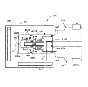
(0049] Referring now to FIG. 2, an illustrative block
diagram of an electrical system 200 including a duplex
electronic circuit breaker 100 in accordance with
embodiments of the present invention is shown. The
electronic circuit breaker 100 may include a power
terminal 219, and in the depicted embodiment, may consist
of a single power terminal 219 on a line side of the
electronic circuit breaker 100. The power terminal 219
may be connectable to a bus 221 (e.g., a single-phase
bus) through an electrical conduction path 222. The
electrical conduction path 222 may be formed in a circuit
breaker panelboard 224 onto which the electronic circuit
breaker 100 is received and mounted, for example. The
power terminal 219 may have a U-shaped form (See terminal
314 in FIG. 3) and may be adapted to be coupled to a stab
(FIG. 11A) provided at a single standard circuit breaker
C.02,w2520.092,
M4)2010/111210
PCT/US2010/028219
location in the circuit breaker panelboard 224.
Optionally, a standard assembly including a lug and lug
screw may be employed. The term "panelboard" as used
herein refers to any component that includes the ability
to distribute electrical power to multiple electrical
circuits, and which is adapted to receive and mount one
or more circuit breakers to protect those electrical
circuits. A panelboard including an electronic circuit
breaker 100 of the invention is shown and described with
reference to FIGs. 11A and 11B herein.
[0050] Again referring to FIG. 2, two separate
electrical circuits 226, 228 including electrical loads
(Load 1 and Load 2) may be connected to the electronic
circuit breaker 100 at a first load terminal 230A and a
second load terminal 230B, one for each electrical
branch. Load 1 and Load 2 may be resistive, inductive,
capacitive, or any combination thereof. The load
terminals 230A, 230B may be integral with the electronic
circuit breaker 100 and may be made of conventional
construction. The protected electrical circuits 226, 228
may also connect to one or more load neutral terminals.
In the depicted embodiment, a first load neutral terminal
216A, second load neutral terminal 216E, and neutral line
pigtail 217, may be provided on the electronic circuit
breaker 100. However, it should be understood that a
single load neutral terminal may be used and each load
neutral connection may be received and secured thereat.
[0051] In more detail, within the duplex electronic
circuit breaker 100, a current (e.g., single-phase
current) from the power terminal 219 may be split into
two electrical branches 232A, 232B. Optionally, there may
be two load terminals, one for each branch. Each of these
electrical branches 232A, 2323 includes their own pair of
electrical contacts 234A, 234B, 236A, 2363 wherein at
least one electrical contact of each set is a moveable
electrical contact (e.g., electrical contacts 236A,
11
C O27543 1O
WO 2010/111210
PCT/US2010/028219
236B). Each branch 232A, 232B may also include its own
tripping mechanisms 238A, 238B including mechanical,
electromechanical and material components to accomplish
circuit breaker tripping, i.e., separation of the
respective electrical contacts 234A, 236A and 234B, 236B
from one another under various circuit conditions.
[0052] For example, the tripping mechanisms 238A, 238B
may each include a cradle, spring, armature, actuator,
magnet and bimetal element, as will be described herein.
Each electrical branch 232A, 232B may include one of the
load terminals 230A, 230B. An electronic processing
circuit 240, which may be a printed circuit board, is
provided in the electronic circuit breaker 100. The
electronic processing circuit 240 may be electrically
coupled to one or more sensors 248A, 248B. Each branch
may include a sensor (e.g., 248A, 248B). The sensors
248A, 248B may sense an electrical condition in one or
more of the branches 232A, 232B (e.g., an electrical
current therein) and provide a signal indicative of the
electrical condition of the branch 232A, 232B, and thus
of the electrical circuits 226, 228, to the electronic
processing circuit 240 in lines 244A, 244B.
[0053] The electronic processing circuit 240 may
process the indicative signal from the sensors 248A, 248B
for one or more of the branches 232A, 232B. In
particular, the electronic processing circuit 240 may
execute an algorithm to determine whether an unwanted
electrical condition exists in one or both of the
electrical circuits 226, 228. For example, the electronic
processing circuit 240 may process the input from the
sensors 248A, 248B according to known algorithms to
determine whether an unwanted electrical condition exists
in one or both of the circuits 226, 228, such as an arc
fault, a ground fault, or other unwanted condition, for
example. In some embodiments, the electronic processing
circuit 240 may simply monitor the circuit condition. The
12
C O27543 1O
WO 2010/111210
PCT/US2010/028219
particular algorithms for determining the existence of an
unwanted electrical condition, and the electronic circuit
components of the electronic processing circuit 240 will
not be further described herein, as they are well known
in the art.
[0054] Upon a determination that an unwanted
electrical condition exists in one or both of the
electrical circuits 226, 228, the electronic processing
circuit 240 may cause one or both of the tripping
mechanisms 238A, 238B, to trip one or more of the
moveable electrical contacts 236A, 2363 as indicated by
the arrow shown extending to the contact arm of the
moveable electrical contacts 236A, 236B. This action
causes the electrical current in the affected electrical
branch 232A, 2323 of the electronic circuit breaker 100
to be interrupted upon separation of the moveable
electrical contact 236A from the stationary contact 234A,
and/or the separation of the moveable electrical contact
2363 from the stationary electrical contact 234B,
depending on whether one or both electrical branches
232A, 2323 are tripped.
[0055] The tripping mechanisms 238A, 238B may further
each include a bimetal member in the current path of each
branch 232A, 232B, which may detect an over current
condition in the protected circuit 226, 228 and also trip
the electronic circuit breaker 100 upon exceeding a pre-
designed and pre-set threshold temperature. Furthermore,
the tripping mechanisms 238A, 2388 may trip the
electronic circuit breaker 100 upon detecting a short
circuit, as will be described further below. The neutral
line pigtail 217 may be connected internally to the load
neutral terminals 216A, 2168 and to the electronic
processing circuit 240. The neutral line pigtail 217 may
also be connected to a panel neutral 249 of the circuit
breaker panelboard 224. Further details of a first branch
of the electronic circuit breaker 100 according to
13
C.02,w2520.02,
WO 2010/111210
PCT/US2010/028219
embodiments of the invention will now be described with
reference to FIG. 3. It should be recognized that the
present invention requires two electrical branches. Both
may be electronic or one may be electronic and the other
one mechanical.
[0056] FIG. 3 illustrates an embodiment of a first
branch of the duplex electronic circuit breaker 100 of
FIG. 1. In the depicted embodiment, the right housing
portion 108 of the circuit breaker 100 is shown. The
right housing portion 108 interfaces with the center
housing portion 106 (FIG. 1) to form an arc chamber 302
which receives and extinguishes the arc created during a
circuit breaker interruption event. A first transverse
sidewall 304 of the arc chamber 302 is formed by an
inside surface of the housing portion 108. The opposing
transverse sidewall of the arc chamber 302 is formed by
the center portion 106 of the housing (See FIG. 1 and
FIG. 8) that interfaces with the housing portion 108. The
arc chamber 302 extends between the first transverse
sidewall 304 and the second transverse sidewall (see 802
in FIG. 8). The transverse direction, as referred to
herein, is illustrated by directional arrow 306.
[0057] In accordance with an aspect of the invention,
a transverse spacing of the transverse sidewalls 304, 802
of the arc chamber 302 may be selected to provide a
transverse arc compression ratio (TACR) which is about
2.0 or less. TACR is defined herein as Ts/d, where Ts is
the transverse spacing between the sidewalls (i.e.,
between sidewall 304 and the sidewall 802 (FIG. 8) of the
center member 106) in a transverse direction and measured
along a path 326 of a moveable electrical contact 310,
and d is a maximum transverse contact face dimension
(e.g., a diameter) across a contact face of the moveable
electrical contact 310, as measured in the transverse
direction 306. Controlling these dimensions in accordance
with the TACR improves arc extinguishment upon separation
14
C.02,w2520.02,
WO 2010/111210
PCT/US2010/028219
of the electrical contacts. Advantageously, this may
enable making all the breaker components in the current
path smaller thereby contributing to an ability to
provide a low profile width.
[0058] The depicted electronic circuit breaker 100
includes a stationary electrical contact 308, shown
dotted because it is located on the opposite side of a
contact terminal 312 shown. The stationary electrical
contact 308 and the moveable electrical contact 310 are
positioned, and included, within the space of the arc
chamber 302. The stationary electrical contact 308 may be
secured (e.g., welded) to the contact terminal 312, which
connects to a power terminal 314 by a suitable electrical
conduit, such as an insulated wire or braided wire, for
example (See 602 of FIG. 7). The stationary contact 308
being provided on the contact terminal 312 is also shown
in FIG. 6. The power terminal 314 may be received over a
stab (FIG. 11A) of a panelboard (FIG. 11A), and may
provide power to the respective braches and the
electrical circuits protected by the electronic circuit
breaker 100. However, it should be understood that the
present invention is applicable to multi-pole electronic
circuit breakers having two or more phases of power
entering wherein such multi-pole electronic circuit
breakers may include two or more power terminals of
conventional construction, for example.
[0059] The arc chamber 302 may be further defined by
end walls 316, 318, in a first crosswise dimension as
indicated by arrow 320, and by end walls 322, 324 in a
second crosswise dimension as indicated by arrow 325.
Upon tripping of the electronic circuit breaker 100, the
moveable electrical contact 310 moves along the travel
path 326 to a maximum as-separated condition (i.e., in a
tripped position, as shown). Tripping of the electronic
circuit breaker 100 moves a contact arm 328, and thus the
moveable contact 310 along the travel path 326. This
C.02,w2520.02,
WO 2010/111210
PCT/US2010/028219
separation causes an electrical arc as the current
provided to an electrical circuit protected by the branch
of electronic circuit breaker 100 is broken, and the arc
chamber 302 may rapidly extinguish the arc.
[0060] Again referring to FIG. 3, the tripping may be
accomplished by hand tripping by a person moving the
handle 112B from an On to an Off position. The throwing
of the handle 112B causes the handle 112B causes a spring
334 (e.g., a coil spring) to exert a force on the contact
arm 328 causing the contact arm 328 to pivot relative to
a lower portion of the handle 112B (see FIG. 8) and moves
the contact arm 328 along the travel path 326 to the
maximum as-separated condition, i.e., a tripped position
(as shown in FIG. 3).
[0061] In other instances, a tripping unit 336 of the
tripping mechanism 331 may trip the electronic circuit
breaker 100 when a persistent over current condition is
experienced by the tripping unit 336 and causes a portion
of the unit to exceed a predetermined temperature
threshold. The tripping unit 336 may include a magnet
338, a bimetal member 339 received alongside of the
magnet 338, and an armature 342. The bimetal member 339
is displaceable (in bending) towards the magnet 338
responsive to increased resistive heating (and a
resultant temperature increase) of the bimetal member
339, such as due to a persistent over current situation.
Additionally, if a short circuit condition is
experienced, the high current through the bimetal member
339 will cause the magnet 338 to attract the armature 342
and thereby tripping the electronic circuit breaker 100.
In the persistent over current instance, the bimetal
member 339 is caused to contact the armature 342 thereby
disengaging a latching surface 344 of the armature 342
from a triggering surface 330T of the cradle 330. In the
short circuit instance, the magnetic attraction of the
armature 342 to the magnet 338 causes the latching
16
C.027$6,2520.02,
WO 2010/111210
PCT/US2010/028219
surface 344 of the armature 342 to disengage from the
triggering surface 330T of the cradle 330. In each
instance, this trips the electronic circuit breaker 100
and causes the cradle 330 to rotate clockwise about a
cradle pivot 332 and cause separation of the electrical
contacts 308, 310 by way of the spring 334 exerting a
force to cause a counterclockwise rotation of the contact
arm 328. Upon tripping, the rotational excursion of the
cradle 330 may be limited by coming to rest on a stop 345
formed on the armature 342 or on the housing portion 108.
[0062] In yet another instance, tripping of the
electronic circuit breaker 100 may be accomplished
automatically upon an electronic processing circuit (FIG.
5A) in the electronic circuit breaker 100 determining
that an unwanted electrical condition exists in one of
the protected electrical circuits attached thereto. This
may be determined for one or both branches upon
processing a signal provided from a sensor 346 coupled to
the electronic processing circuit. The sensor 346 may be
any suitable sensor for determining an electrical
condition within the electronic circuit breaker 100. For
example, the sensor 346 may be a coil type sensor. The
sensor 346 may be provided adjacent to an electrical
strap 348 extending between, and electrically connecting,
the load terminal 340 to a first end of the bimetal
member 339. In the depicted embodiment, the electrical
strap 348 is a metal strap, which may be bent in the
crosswise directions 320, 325 at various locations along
its length. The electrical strap 348 may have a cross-
sectional area, which is rectangular, for example. Other
shapes may be provided. An end of the bimetal member 339
may be secured to the electrical strap 348, such as by
welding, for example. The electrical strap 348 may also
be welded to the load terminal 340. In the depicted
embodiment, the electrical strap 348 may extend past the
bimetal member 339 and include a cantilevered portion
348A. This cantilevered portion 348A may be contacted by
17
C.027$6,2520.092,
WO 2010/111210
PCT/US2010/028219
a calibration screw 362 to adjust a position of the
bimetal member 339 relative to the armature 342 thereby
calibrating the tripping unit 336. Also shown in FIG. 3
is a pivot element 349 which supports the magnet 338 and
allows limited pivoting thereof. The limits of the
pivoting are set by stops formed in the housing portion
108, for example. The pivot element 349 may be a separate
component or a part of the housing portion 108. A
calibration screw 362 may also be mounted in a base of
the pivot element 349.
[00631 Again referring to the controlled tripping
aspect of the invention, upon determining that an
unwanted condition exists in the protected circuit (e.g.,
an arc fault, or a ground fault, etc.), the electronic
processing circuit 540 (FIG. 6) may cause an actuator 350
to move the armature 342. For example, the armature may
be moved at a first end thereof, and cause a
disengagement of the latching surface 344 from the
triggering surface 330T of the cradle 330. This, in the
manner previously discussed, separates the electrical
contacts 308, 310 from one another and interrupts the
protected electrical circuit connected to the branch.
These tripping events, due to over current, short
circuit, or experiencing an unwanted electrical condition
in the protected electrical circuit, may cause an
electrical arc, which may be rapidly extinguished within
the arc chamber 302.
[003641 In the depicted embodiment, the actuator 350
may be an electromagnet, which may include a magnetic
pole, which, upon energizing the actuator 350,
magnetically attracts and moves the armature 342. In this
embodiment, the armature 342 is made from a ferromagnetic
material, such as steel. However, any suitable
magnetically permeable material may be used. In optional
embodiments, the actuator 350 may be a solenoid or other
type of actuator, which is adapted to move the armature
18
C.027$6,2520.02,
WO 2010/111210
PCT/US2010/028219
342 upon command from the electronic processing circuit
540 (FIG. 5A). In the presently depicted embodiment, the
actuator 350 is located in a pocket formed adjacent to
the wall 316. In operation, engaging the armature 342 at
the first end enables the actuator 350 to be located
along a back side of the circuit breaker 100 opposite
from the handle side, and within the space formed by an
interaction of the first housing portion 108 and the
center housing portion 106 (FIG. 1). This enables
components of the triggering mechanism 331 (e.g., cradle)
to be made relatively smaller, and frees up space located
centrally within the circuit breaker 100 to compactly
house the other tripping components and electronic
processing circuit 540 (FIG. 5A) thereby contributing to
achieving a low profile.
[00651 Again referring to FIG. 3, and in accordance
with another aspect, the arc chamber 302 may include one
or more recesses 352 formed (e.g., molded) into the first
transverse sidewall 304. Such recesses 352 may be
optionally or additionally provided in the second
sidewall 808 (FIG. 8), as well. These recesses 352 may
receive a portion of the electrical arc generated by
separation of the electrical contacts 308, 310 and
promote rapid arc extinguishment within the electronic
circuit breaker 100. In the depicted embodiment, multiple
recesses 352 comprising pockets or holes formed (e.g.,
molded) into in the transverse sidewall 304 are provided
wherein the openings thereof are located on the
sidewalls.
[0066] In particular, the recesses 352 may be provided
alongside of the travel path 326, and in some
embodiments, on both sides of the travel path 326 in the
first crosswise direction 320. Again, rapid arc
extinguishment may contribute to being able to reduce the
size of the current carrying components and, thus, may
enable lowering a transverse profile of the electronic
19
CA 02756125 2014-02-24
54106-967
circuit breaker 100. A further description of the arc
chambers may be found in co-assigned U.S. Patent
Application entitled "Circuit Breaker Arc Chamber And
Method For Operating Same" contemporaneously filed with
the present application.
[00671 With reference to FIGs. 4A-4E, an embodiment of
a tripping mechanism 400 according to another broad
aspect of the invention is described, as are components
thereof. The tripping mechanism 400 may include a cradle
430, having a triggering surface 430T, which when tripped
(e.g., due to over current, short circuit, or by
controlled actuation), disengages from a latching surface
444 located at a second end 4433 of an armature 442 and
rotates clockwise about a cradle pivot 432. The cradle
pivot 432 is shown in FIG. 4A, while the rest of housing
portion, except for housing extension 455 and housing
projection 458 on housing portion 408, is not shown for
clarity. As described above, this rotation causes a
spring 434 (e.g., a coil spring) to exert a force to move
the contact arm 428 along the travel path 426 (shown
dotted) to the maximum as-separated condition, i.e., a
tripped position. The maximum as-separated position may
be determined by a stop, such as the end wall 324 (See
FIG. 3). Other types of stops may be used.
[00683 The tripping mechanism 400 may also include a
low-profile tripping unit 436, also shown in FIGs. 43 and
4C, which is adapted to trip the circuit breaker under a
variety of conditions. For example, the tripping unit 436
may trip the circuit breaker when the tripping unit 436
experiences a persistent over current condition or upon
experiencing a short circuit condition, or upon active
actuation by the actuator 350. The tripping unit 436 may
include a magnet 438, a bimetal member 439 received
alongside of the magnet 438, and an armature 432. In the
depicted embodiment, as best shown in FIG. 43, the
C.02,w2520.092,
M4)2010/111210
PCT/US2010/028219
bimetal member 439 is received between sidewalls of the
magnet 438. The bimetal member 439 may be generally
rectangular in shape and may include two metals with
different thermal expansion coefficients, such that an
end 4393 of the bimetal member 439 is displaceable
(flexes) towards the magnet 438 responsive to persistent
over current exposure, which causes a threshold
temperature to be exceeded due to resistive heating of
the bimetal member 439. This causes the second end 439B
of the bimetal member 439 to contact an engagement
portion (e.g., a bent tab 442C) of the armature 442 at
the second end 443B of the armature 442 thereby
disengaging the triggering surface 430T of the cradle 430
from a latching surface 444 of the armature 442 at the
second end 4438. In turn, this causes rotation of the
cradle 430, tripping of the circuit breaker, and movement
of the contact arm 428 and moveable electrical contact
410 along the travel path 426 thereby separating the
moveable electrical contact 410 from a stationary contact
(not shown in FIG. 4A).
[0069] In the case of a short circuit being
experienced (e.g., very high current) in the protected
circuit, a high current flows through the bimetal member
439. This induces a magnetic field in the magnet 438
which causes the armature 442 be attracted to the
sidewalls of the magnet 438 and also to pivot on the
magnet 438. This motion disengages the latching surface
444 of the armature 342 from the triggering surface 430T
of the cradle 430 and trips the circuit breaker including
the tripping mechanism 400.
[0070] In the depicted embodiment, an electrical strap
448 may be provided and connected to a component of the
tripping unit 436. In some embodiments, the electrical
strap 448 may extend between, and electrically connect,
the load terminal 440 to the bimetal member 439 at a
first end 439A thereof. The electrical strap 448 may be
21
C.02,w2520.092,
M4)2010/111210
PCT/US2010/028219
as described in the previous embodiment, and may be
securely fastened to the first end 439A of the bimetal
member 439 (e.g., such as by welding, for example). The
electrical strap 448 may also extend through the load
terminal 440 and may be also be welded thereto. A tab 445
may extend through the load terminal 440 and may be bent.
The tab 445 may be used to position the electrical strap
448 and load terminal 440 into a pocket or slot formed in
the housing portion (e.g., housing portion 108), for
example. In some embodiments, the electrical strap 448
may extend beyond the bimetal member 439 thereby forming
a cantilevered end 448A beyond the connection between the
bimetal member 439 and the electrical strap 448. Exerting
a force on the cantilevered end 448A by threading
calibration screw 462 against the housing portion 408
causes the cantilevered end 448A to flex. Upon flexure,
the electrical strap 448 (e.g., the cantilevered end
448A) may contact a projection 458. This, in turn,
elastically flexes the electrical strap 448 and causes
the second end 439B of the bimetal element 439 to adjust
its position relative to the location of engaging portion
442c of the armature 442. Accordingly, this feature may
be used to accomplish calibration of the tripping unit
436.
(0071] In the case of an electronic circuit breaker,
the tripping mechanism 400 may also include an actuator
450 (e.g., an electromagnetic actuator) which may have a
magnetizable pole 451 adapted to attract the armature
442. The actuator 450 may be positioned adjacent to the
travel path 426 of the moveable contact 410 on a side of
the circuit breaker opposite from the location of the
handle 112B.
[0072] In the depicted embodiment, the actuator 450
may engage the armature 442 at the first end 443 upon
command from the electronic processing circuit 540 (FIG.
5A), and magnetically attract and pull the armature 442
22
C O27543 1O
WO 2010/111210
PCT/US2010/028219
towards the magnetizable pole 451 (e.g., in the direction
of arrow 454). This causes the armature 442 to pivot
about a pivot location 452. In this embodiment, the pivot
location 452 on the armature 442 is provided between the
first end 443 and second end 443B of the armature 442.
According to some embodiments, the armature 442 may pivot
at a location on the magnet 438. In particular, the
armature 442 may pivot on a portion of the magnet 438.
The pivot location 452 on the magnet 438 may be formed by
tabs 438A provided on either side of the first end 438B
of the magnet 438 as shown in FIGs. 43 and 4C. Tabs 442D
formed on the armature 442 may be received in the slots
formed by tabs 438A (See also FIGs. 4B-4E). The tabs 442D
may be smaller (thinner) than the slots formed by tabs
438A, and, thus, may provide a pivot at the pivot
location 452 such that the armature 442 may pivot
relative to the magnet 438. This movement of the armature
442 causes a compression of a spring 456 (e.g., a coil
spring) mounted on a spring receiver 442E abutting
housing extension 455, and thereby disengagement of the
latching surface 444a from a triggering surface 430T of
the cradle 330. This, in the manner previously discussed,
causes the cradle 430 to rotate clockwise, moving the
contact arm 428, and separating the moveable electrical
contact 410 from the stationary contact (not shown in
FIG. 4A). As shown in FIGs. 4A and 4C, an electrical
conduit 457 (e.g., a braided line) may connect the second
end 4393 of the bimetal member 439 to the contact arm
428.
(0073] Now referring to FIGs. 5A and 58, further
subassembly views of are provided. In FIG. 5A, the
previously-described portion of the circuit breaker 100
of FIG. 3 is provided as a subassembly 500, further
including an electronic processing circuit 540 installed
to contact and abut the right housing portion 108. The
electronic processing circuit 540 may be provided in the
form of a printed circuit board, for example. The
23
C.027$6,2520.02,
WO 2010/111210
PCT/US2010/028219
electronic processing circuit 540 may be mounted in a
pocket of the housing portion 108 or on a feature formed
in the electronic processing circuit 540 (e.g., a hole)
and is sandwiched between the portions 108, 106. Further,
the subassembly 500 may include one or more load neutral
terminals 116A, 1163, at least one of which is partially
retained and received in a pocket of the right housing
portion 108. The neutral terminals 116A, 116B may be
interconnected to the electronic processing circuit 540
through electrical wires 560, 561 and provided as an
electrical subassembly with the electronic processing
circuit 540. Further, a neutral line pigtail 117 may
interconnect with the electronic processing circuit 540
and extend out of a bottom of the housing portion 108.
Sensor 346 may be connected to the electronic processing
circuit 540 via a wire and electrical connection (not
shown). Electrical conduits 562A, 562B, and 563 are shown
connected to the load neutral terminals 116A, 1163 and
load terminal 340. Such conduits 562A, 562B, 563 do not
form a part of the present electronic circuit breaker
100, but are part of the protected circuit and are
included to illustrate connections to the protected
circuit. The conduits 562A, 5628, 563 may be any suitable
gauge required for the electrical circuit, such as AWG 8,
AWG 10, AWG 12 or AWG 14, for example. The tripping
mechanism 531 is shown in multiple positions to
illustrate the motion of the contact arm 528.
[00743 In FIG. 5B, the previously described
subassembly 500 is further assembled with additional
breaker components to form a second subassembly 565. In
particular, the center housing portion 106 is provided in
an abutting relationship to the right housing portion
108, and handle 112A is provided. The load neutral
terminal 116A may be received in a pocket 567 of the
center housing portion 106. A hole 568 formed in the
housing portion 106 provides accessibility to the
electronic processing circuit 540 by the other branch (to
24
C.027$6,2520.092,
WO 2010/111210
PCT/US2010/028219
be described further herein). The power terminal 314 is
received in a pocket 569 formed in the center housing
portion 106. Together, the right housing portion 108 and
center housing portion 106 interface to provide a slot
570 which may receive a stab of a panelboard (FIG. 11B).
[00751 FIG. 6 is an exploded view of the various
components of the duplex electronic circuit breaker 100
according to embodiments of the present invention.
Illustrated are the left housing portion 104, center
housing portion 106 and right housing portion 108. Also
illustrated is the electronic processing circuit 540
sandwiched between the right and center housing portions
108, 106. As should be apparent, the circuit breaker
components included in the second branch in the center
housing portion 106 may be the same as the first branch
included in the right housing portion 108, as were
described in FIG. 3. For example, they may include
identical handles 112A, 112B, contact arms 328, 328A,
cradles 330, 330A, springs 334, 334A, magnets 338, 338A,
and armatures 342, 342A. The center housing portion 106
may include a load terminal 340A received in a pocket
therein, in a similar manner as the load terminal 340 is
received in the right housing portion 108. The center
housing portion 106 may include a load neutral terminal
116A received in a pocket therein, in a similar manner as
the load neutral terminal 116B is received in the right
housing portion 108. As shown, the two housing portions
106, 108 abut and engage each other and retain the
terminals 116B and 340 in the electronic circuit breaker
100. Likewise, the portions 104, 106 may abut and engage
each other and retain the terminals 116A and 340A in the
electronic circuit breaker 100.
(00761 The power terminal 314 may include an
electrical conduit 602 which electrically connects to the
contact terminal 312. Contact terminal 312 may be
received through the center housing portion 106 and may
C.02,w2520.092,
WO 2010/111210
PCT/US2010/028219
include the stationary electrical contacts 308, 308A for
each pole (on either end of the contact terminal 312).
Optionally, the power terminal 314 may be connected to
separate contact terminals, each including a stationary
electrical contact 308, 308A. In the depicted embodiment,
the electronic processing circuit 540 has mounted
thereon, on opposite sides thereof, a first actuator 350
which is received in a pocket 604 formed in the right
housing portion 108 and second actuator 350A which is
received in a through hole 605 in the center housing
portion 106. The actuators 350, 350A may be identical
electromagnetic actuators, and may each include
magnetizable pole 451 (only one shown in FIG. 6) which is
positioned at a location adjacent to the first end 443,
443A of the armatures 442, 442A. Although not shown,
sensors 346, 346A may be sub-assembled and connected to
the electronic processing circuit 540 as an integral unit
by conduits (not shown) and the sensor 346A may be
received through the hole 568 in center housing portion
106 and received on the other side of center housing
portion 106.
[00771 FIGs. 7 and 8 illustrate views of the center
housing portion 106 from two different sides to
illustrate the positioning and orientation of the breaker
components of the two branches of the electronic circuit
breaker 100. For example, in FIG. 7, the contact terminal
312 including the stationary electrical contact 308A is
shown installed through the center housing portion 106.
Also shown is the connection and positioning of the
conduit 602 between the contact terminal 312 and the
power terminal 314. The electrical conduit 560 may be
connected to the load neutral terminal 116A as shown by
passing through a hole 704 in the center housing portion
106. The conduit 560 may be secured (e.g., by soldering)
to a connector 706, which may be received through, or
otherwise connected (e.g., by welding) to the load
neutral terminal 116A.
26
cAmw2520.02,
WO 2010/111210
PCT/US2010/028219
[00781 In FIG. 8, the contact terminal 312 including
the stationary electrical contact 308 is shown installed
through the center housing portion 106. Also shown is the
positioning of the power terminal 314 in a pocket formed
in the center housing portion 106. On this side,
electrical conduit 561 may be connected to the load
neutral terminal 116B as shown. The electrical conduit
561 may be secured (e.g., by soldering) to a connector
806, which may be received through, or otherwise
connected (e.g., by welding) to the load neutral terminal
116B. The neutral line pigtail 117 is shown received in
a recess formed in the center housing portion 106. The
center housing portion 106 and right housing portion 108
(FIG. 1) may engage each other to position and secure the
neutral line pigtail 117 in its position, as shown. An
electrical conductor 808 may attach to the electronic
processing circuit 540 and may connect to the conductor
561. Also shown is the connection of the test button onto
the electronic processing circuit 540. In some
embodiments, the electronic processing circuit 540 may
include a conductor 810 extending therefrom, which may be
appropriately positioned such that upon installation of
the electrical strap 348, contacting engagement with the
electrical strap 348 is made. This may provide power to
the electronic processing circuit 540. A similar
connection to the electrical strap on the 348A may be
made on the other side.
[00791 Also clearly illustrated in FIG. 7 and 8 are
the connections of the electrical straps 348, 348A to the
load terminals 340, 340A and to the first ends of the
bimetal members 339, 339A, as well as the pivoting
element 349, 349A. Likewise, electrical conduits 712,
712A (e.g., braided wires) are shown electrically
connecting the bimetal members 339, 339A to the contact
arms 328, 328A. In FIG. 8, it is illustrated that the
electronic processing circuit 540, in the form of a
printed circuit board, is received into a pocket formed
27
C.02,w2520.092,
WO 2010/111210
PCT/US2010/028219
in the center housing portion 106. Accordingly, the
printed circuit board is accessible to the electrical
components (e.g., sensor 346, 346A) on either side of the
central housing member 106. Additionally, as can be seen
from these two views, upon installation of the printed
circuit board, the actuator 350, 350A are positioned to
engage with the armatures 342, 342A. It should be
understood that the printed circuit board may be split
into multiple pieces and provided at different locations
within the electronic circuit breaker wherein different
functions may be provided on each board piece.
[0080] FIGs., 9A and 9B are perspective views of the
electrical harness assembly 900. The harness assembly 900
may include the neutral line pigtail 117 having a first
end 117A and a second end 117B. The first end may be
secured (e.g., by soldering) to a tang 902 of the neutral
line pigtail 117, whereas the second end 117B may be
adapted to be attached to a panelboard neutral. As
described above, electrical conduits 560, 561 attach to
the load neutral terminals 116A, 116B by way of
connectors 706, 806. Another end of the electrical
conduits 560, 561 may attach (e.g., by soldering) to the
tang 902. Conductor 808 may be attached to the electronic
processing circuit 540.
[0081] FIG. 10 is a flowchart illustrating a method of
installing an electronic circuit breaker according to an
aspect of the present invention. The method includes
providing a panelboard including a plurality of standard
circuit breaker mounting locations in 1002. Each of the
standard circuit breaker mounting locations may include a
single stab. The method 1000 further provides, in 1004,
mounting an electronic circuit breaker including two
branches to occupy a single standard circuit breaker
mounting location in the panelboard. In some embodiments,
a power terminal of the electronic circuit breaker may be
coupled to the single stab at each standard circuit
28
C.027$6,2520.02,
WO 2010/111210
PCT/US2010/028219
breaker mounting location. A standard circuit breaker
mounting location on a panelboard is a space in the
panelboard that is adapted to receive a single, standard
width, single-pole circuit breaker. For example, a
panelboard may be designed to have 6, 8, 12, 16, 32 or 54
standard circuit breaker locations. Panelboards are
designed to meet National Electrical Code, NEMA, and
Federal Specifications. As should be recognized, because
the profile width of the present electronic circuit
breaker 100 including two branches is the same as a
conventional single-pole circuit breaker, it is now
possible to provide greater than in load terminals within
the panelboard, where n is a number of standard breaker
mounting locations within the panelboard.
[0082] FIGs. 11A and 11B illustrate an electrical
panelboard system 1100 including a panelboard 1124, which
may include one or more electronic circuit breakers 100
having two branches mounted therein (only one breaker
shown). The panelboard 1124 may be received in a panel
box 1100A (only a portion shown in FIG. 11B). The panel
box 1100A may include a cover, a latching door, and other
panel box components (all not shown). The panelboard 1124
includes a plurality of standard circuit breaker mounting
locations 1101-1112 (e.g., 1 inch standard circuit
breaker locations) thereon. In the depicted embodiment,
twelve standard mounting locations are shown. However, a
panelboard including more or less standard mounting
locations may be provided, such as 4, 8, 16, 32, or 54
standard mounting locations, for example. Each standard
circuit breaker mounting location 1101-1112 may include a
single stab 1127 or a stab 1127 shared by circuit
breakers arranged in an end to end configuration across
the panel box 1100A. In the depicted embodiment, six
stabs 1127 are provided, and each is shared by two
circuit breakers, for a total of twelve standard circuit
breaker locations. The electronic circuit breaker 100 is
mounted to a single one of the stabs 1127 and may receive
29
C.02,w2520.02,
WO 2010/111210
PCT/US2010/028219
a single phase of power therefrom.
[0083] Each of the one or more electronic circuit
breakers 100 according to the invention exhibits a low
profile having a maximum transverse width (Wt) in the
transverse direction 306. In particular, Wt may be less
than about 1 inch (less than about 25.4 mm) such that the
electronic circuit breaker 100 may fit within, and
occupy, a single one of the plurality of standard
panelboard mounting locations 1101-1112 (the electronic
circuit breaker 100 being installed in standard mounting
location 1109). As can be seen, within each standard
circuit breaker location where an electronic circuit
breaker 100 is installed, two load terminals 340, 340A
may be accommodated. Furthermore, each electronic circuit
breaker 100 may include two load neutral terminals (see
FIG. 1). The duplex electronic circuit breaker 100 of the
invention may be mounted to occupy a single standard
circuit breaker mounting location in the panelboard in
the same manner as a standard 1-inch single-pole
mechanical circuit breaker may be mounted, for example.
Mounting the electronic circuit breaker 100 to the stab
1127 couples the power terminal 314 (FIG. 3) of the
electronic circuit breaker 100 to the single-phase power
bus so that each branch receives power. As was discussed
above, there may be lug assemblies used rather than
stabs. In such a case, the electronic circuit breaker may
include one or more power terminal lug assemblies.
[0084] It should now be apparent that utilizing the
electronic circuit breaker 100 within the panelboard may
provide greater than ln load terminals within the
panelboard where n is a number of standard breaker
locations within the panelboard. In some embodiments, 2n
load terminals may be provided. For example, for a
standard 12 breaker panelboard (shown in FIG. 11), 24
load terminals may be provided. Other numbers of load
terminals between 13 and 24 may be provided based upon
C.02,w2520.02,
WO 2010/111210
PCT/US2010/028219
the combination of circuit breakers installed in the
panelboard. For example, the electronic circuit breaker
100 including two branches of the invention may be
installed alongside of any conventional circuit breaker.
[0085] FIG. 12A illustrates another embodiment of a
tripping unit 1200 for a circuit breaker. The tripping
unit 1200 is similar to the tripping unit 436 described
with reference to FIG. 4A, but differs in that an
actuator 1250 is formed as part of the magnet 438, such
that the magnetizable pole 1251 of the actuator 1250 may
magnetically attract the armature 1242. In the depicted
embodiment, the actuator 1250 is an electromagnet and is
formed on an end of the magnet 1238. However, it should
be apparent that the actuator 1250 may be positioned in
any manner as long as it is connected to the magnet 1238,
and such that a suitable attraction force may be
generated to attract the armature 1242 and thereby trip
the circuit breaker. Optionally, as shown in FIG. 123,
the coil 12503 may be mounted on a bent tab of the
armature 1242B on the second end thereof and energized to
attract to the magnet 1238B wherein the bent tab faces
the magnet 1238B and functions as a pole.
[0086] In this embodiment, the actuator 1250 is an
electromagnet including a magnetizable pole 1251 formed
from a portion of the magnet 1238. In particular, the
magnetizable pole 1251 may be formed from a bent tab on
an end of the magnet 1238. A series of wire windings may
be wound about the magnetizable pole 1251 to form a coil
1252. In some embodiments, the coil 1252 may be
separately formed and slid over the pole 1251 and secured
thereto by adhesive, for example. The number of wire
windings provided will be chosen to provide a suitable
force to displace the armature 1242 a sufficient distance
to cause breaker tripping and to ensure clearance with
the other components of the tripping unit. The electrical
leads from either end of the coil 1252 may be attached to
31
C.02,w2520.02,
WO 2010/111210
PCT/US2010/028219
an electronic processing circuit (not shown in FIG. 12A) .
[0087] In the described embodiment of FIG. 12A, a
command from an electronic processing circuit (not shown
in FIG. 12A) to the actuators 1250 may induce a magnetic
field in the magnet 1238 and produce an attraction force
between the magnet 1238 and the armature 1242. This
causes movement of the armature 1242 (e.g., pivoting
about the magnet 1238) at pivot location 1252, a
sufficient distance to cause the latching surface 444 of
the armature 1242 to disengage from the triggering
surface 430T of the cradle 430 (only a portion of cradle
430 shown). In this embodiment, a tail on the armature
1242 beyond the spring 456 may be removed.
[0088] Together, FIGs. 13A-13C illustrates another
embodiment of a tripping mechanism 1300 for a circuit
breaker. This embodiment is similar to the FIG. 4A
embodiment, but is designed for use in a single-pole
electronic circuit breaker. In this embodiment, in a like
manner as in FIG. 4A, the tripping mechanism 1300
includes a tripping unit 1336 having a magnet 1338, a
bimetal member 1339 received alongside of the magnet
1338, and an armature 1342. The armature 1342 is
pivotable at pivot location 1352 on the magnet 1338. In
this embodiment, the pivot location 1352 is formed on the
magnet 1338 by tabs 1338A formed on either side of the
magnet 1338 in the same manner as is shown in FIG. 4B and
4C. In this embodiment, the armature 1342 includes tabs
1342D, which may be shoulders formed on the armature 1342
(See FIG. 13C) which may rest in a slot formed by the
tabs 1338A. In addition, the armature 1342 may include an
engagement portion 1342C which is engageable with the
bimetal member 1339 at a moveable end 1339C of the
bimetal member. A spring 1356 may be provided on a spring
receiver 1342E of the armature 1342 to bias the armature
1342 away from the magnet 1338.
[0089] In some embodiments, a tab 1342F may be
32
C.02,w2520.02,
WO 2010/111210
PCT/US2010/028219
provided on a side of the armature 1342 and is adapted to
be contacted by an actuator (not shown) of the type
described herein when the tripping unit 1336 is used
within an electromagnetic circuit breaker.
[0090] The armature 1342 may also include a latching
surface 1344 formed on a tab extending from a body of the
armature 1342, which is adapted to engage a tripping
surface 1330T on a cradle 1330. In operation, when a
persistent over current situation is encountered,
engaging portion 1342C will be engaged and contacted by
the moveable end 1339C of the bimetal member 1339 as it
moves closer to the magnet 1338. This disengages the
latching surface 1344 from the tripping surface 1330T of
the cradle 1330 (only a portion shown in FIG. 13B) and
thereby the tripping mechanism 1300 trips the circuit
breaker by causing the cradle 1330 to rotate clockwise
and move the contact arm 1328 and the moveable contact
1310 away from the stationary contact 1308. As shown, a
tab 1360 on the contact arm 1328 may rotate within a hole
1361 in the backside of the handle 1312. As shown, an
electrical strap 1348 may connect between the load
terminal 1340 and the first end 1339B of the bimetal
member 1339, and may be securely fixed to each (e.g., by
welding). A calibration screw 1362 engages the electrical
strap 1348 and functions to calibrate a response of the
tripping unit 1336. Housing portion 1365 retains the
various components (e.g., handle 1312, magnet 1338) load
terminal 1340, in pockets formed by interaction of the
housing portion 1365 and a conventional cover portion
(not shown).
[0091] FIGs. 14A, 14B and 14C illustrate another
embodiment of a tripping mechanism 1400 for a circuit
breaker. This embodiment is similar to the FIG. 13A-13C
embodiment, but differs in the locations of the latching
surface 1444 and the calibration screw 1462. In this
embodiment, in a like manner as in FIG. 13A-13C, the
33
C.02,w2520.092,
WO 2010/111210
PCT/US2010/028219
tripping mechanism 1400 includes a tripping unit 1436
having a magnet 1438, a bimetal member 1439 received
alongside of the magnet 1438, and an armature 1442. The
armature 1442 is also pivotable on the magnet 1438, and
the pivot is formed in the same way as described in FIGs.
13A-13C. In the same manner as in the previous
embodiment, the armature 1442 may include an engagement
portion 1442C, which is engageable with the bimetal
member 1439 at a moveable end 1439C thereof.
[0092] In some embodiments, such as in electronic
circuit breakers, a tab 1442F may be provided on a side
of the armature 1442 to be contacted by an actuator, as
discussed above. In the depicted embodiment, the armature
1442 may include a latching surface 1444 formed on a tab
extending from a body of the armature 1442 at a terminal
end that is the farthest away from the pivot location
1452. As described above, the latching surface 1444
disengages from a tripping surface 1430T on a cradle 1430
(only a portion shown in FIG. 143) when a temperature
threshold due to a persistent over current is
encountered. As before, engaging portion 1442C is
contacted by the moveable end 1439C of the bimetal member
1439. This trips the circuit breaker as described above.
[0093] As shown in FIG. 14A, an electrical conduit
1468 may connect between the load terminal 1440 and an
electrical strap 1448, which is securely fixed to a fixed
end 1439B of the bimetal member 1439 (e.g., by welding).
A calibration screw 1462 engages the electrical strap
1448 and a head of the screw 1462 engages a housing
portion 1465. When the electrical strap 1448 is flexed in
bending, this moves the moveable end 1439C of the bimetal
member 1439 and functions to calibrate a response of the
tripping unit 1436. A sensor 1446 may be provided to
sense an electrical condition (e.g., current) in the
electrical conduit 1468 and may be coupled to the
electronic processing circuit (not shown).
34
C.02,w2520.02,
WO 2010/111210
PCT/US2010/028219
(00941 FIGs. 15A-15D illustrates yet another
embodiment of a tripping mechanism 1500 for a circuit
breaker. In this instance, the depicted tripping
mechanism 1500 is adapted for use in an electronic
circuit breaker. This embodiment is similar to the FIGs.
14A-14C embodiment, but differs in the configuration of
the engagement portion 1542C, the location of the
calibration screw 1562, and the location of the actuator
1550. In this embodiment, in a like manner as in FIG.
14A-14C, the tripping mechanism 1500 includes a tripping
unit 1536 having a magnet 1538, a bimetal member 1539
received alongside of the magnet 1538, and an armature
1542. The armature 1542 is pivotable on the magnet 1538,
and the pivot is formed in the same way as described in
FIGs. 13A-13C and 14A-14C. Furthermore, the armature 1542
may include an engagement portion 1542C at the second end
1543B, which is engageable with the bimetal member 1539
at a moveable end 1539C thereof. In this embodiment, the
pivot element 1449 is formed as part of the housing 1565
and allows pivoting of the magnet 1538 thereabout and
towards the armature 1542. In an optional embodiment, the
pivot member 1538 may be inserted in a pocket formed in
the housing 1565 and may be formed of a more rigid
material, such as steel, for example. Pivoting may be
limited by stops or pockets engaging the magnet 1538 at
the desired pivoting limits (not shown).
100951 In this embodiment, which is adapted for use
with an electronic circuit breaker, such as the
electronic circuit breaker including two branches
described herein, a first end 1543 may be provided on the
armature 1542 to be engaged by an actuator 1550, such as
an electromagnetic actuator. In the depicted embodiment,
the armature 1542 may include a latching surface 1544
formed on a tab extending from a body of the armature
1542 at a second end 1543B. As described above, the
latching surface 1544 engages a tripping surface 1530T on
a cradle 1530 (only a portion shown in FIG. 15B), and
C.02,w2520.092,
M4)2010/111210
PCT/US2010/028219
when a temperature threshold due to a persistent over
current condition is encountered, engagement portion
1542C is engaged and contacted by the moveable end 1539C
of the bimetal member 1539. This pivots the armature 1542
about tabs 1542D (only one of two shown in FIG. 15D) and
about the pivot location 1552 and trips the circuit
breaker, as described above.
[0096] In the case of an arc fault, ground fault or
other unwanted electrical condition being sensed, the
actuator 1550 may actuate the armature 1542 by way of
magnetic attraction to pole 1551, which pivots the
armature 1542 about pivot location 1552 and thereby
disengages latching surface 1544 from tripping surface
1530T. As in the previous embodiments, an electrical
strap 1548 may be provided and coupled to a load terminal
1540 and the bimetal member 1539. A calibration screw
1562 may contact a cantilevered end 1548A of the
electrical strap 1548 which extends beyond the bimetal
member 1539 and may be adjusted to calibrate the tripping
unit 1536. Additionally, a sensor 1546 may be provided to
sense an electrical condition in the electrical strap
1548. The electrical strap 1548 may be encircled by the
sensor 1546. Any suitable sensor may be used.
[0097] FIG. 16 illustrates yet another embodiment of a
tripping mechanism 1600 for a circuit breaker. In this
instance, the depicted tripping mechanism 1600 is adapted
for use in a duplex electronic circuit breaker. This
embodiment is similar to the FIG. 3 embodiment, but
differs in the configuration of the electrical strap
1648, the location of the calibration screw 1662, and the
configuration of the arc chamber 1602. In this
embodiment, in a like manner as in FIG. 3, the tripping
mechanism 1600 includes a tripping unit 1636 having a
magnet 1638, a bimetal member 1639 received alongside of
the magnet 1638, and an armature 1642. The armature 1642
is pivotable on the magnet 1638, and the pivot is formed
36
C.02,w2520.02,
WO 2010/111210
PCT/US2010/028219
in the same way as described in FIGs. 4A and FIGs. 15A-
15D. As before, the armature 1642 may include an
engagement portion 1642C at the second end 1643B, which
is engageable with the bimetal member 1639 at a moveable
end 1639C thereof.
[0098] In this embodiment, a first end 1643 may be
provided on the armature 1642 to be engaged by an
actuator 1650, such as an electromagnetic actuator. In
the depicted embodiment, the armature 1542 may include a
latching surface 1644 formed on a tab extending from a
body of the armature 1642 at the second end 1643B. The
latching surface 1644 engages a tripping surface 1630T on
a cradle 1630 in an un-tripped condition. When a
temperature threshold due to a persistent over current
condition is encountered, engagement portion 1642C is
engaged and contacted by the moveable end 1639C of the
bimetal member 1639. This pivots the armature 1642 about
the pivot location 1652 on the magnet 1638 and trips the
circuit breaker. In the case of a short circuit
condition, current flow through the bimetal element 1639
may induce a magnetic field in the magnet 1638 thereby
causing the armature 1642 to be attracted to the
sidewalls of the magnet 1638. This pivots the armature
1642 about the pivot location 1652 which, in turn,
disengages the latching surface 1644 from the tripping
surface 1630T on a cradle 1630.
[0099] In the case of an arc fault, ground fault or
other unwanted electrical condition being sensed by an
electronic processing circuit (not shown), the actuator
1650 may be commanded to actuate the armature 1642 by way
of magnetic attraction to pole 1651. As described above,
this pivots the armature 1642 about pivot location 1652
and disengages the latching surface 1544 from the
tripping surface 1530T. As in the previous embodiments,
an electrical strap 1648 may be provided and coupled to a
load terminal 1640 and the first end 16393 of the bimetal
37
WO 2010/111210
PCT/US2010/028219
member 1539.
[moo] As shown, the electrical strap 1638 may pass
closely alongside of the magnet 1638 and then extend
towards the load terminal 1640 where the electrical strap
1638 may be retained between one or more retaining
portions 1663 of the housing portion 1608. A calibration
screw 1662 may contact a cantilevered end 1648A of the
electrical strap 1648 which extends beyond the bimetal
member 1639. This cantilevered end 1648A may be adjusted
to calibrate the tripping unit 1636. Additionally, a
sensor 1546 may be provided to sense an electrical
condition in the electrical strap 1548. The electrical
strap 1548 may be encircled by the sensor 1546. Any
suitable sensor may be used. This configuration of the
tripping unit 1636 and electrical strap 1648 may allows
large spaces 1665 to be made available for the electronic
components, and may contribute to the low profile of the
circuit breaker.
[00101] FIGs. 17A-17B illustrates various components of
another exemplary electronic circuit breaker 1700
including two electrical branches according to
embodiments of the invention. This embodiment is similar
to the FIG. 6 embodiment, and includes tripping
mechanisms 1701, 1701A for each branch of the type
described in FIG. 16. The electronic circuit breaker 1700
also includes left, center, and right housing portions
1704, 1706 and 1708, respectively. The difference in this
embodiment is that electronic processing circuit for each
branch is provided on separate printed circuit boards
1240, 1240A. In this embodiment, an actuator 1750, 1750A
for each branch is mounted on each printed circuit board
1740, 1740A. Thus, as should be apparent that upon
assembly, each circuit board 1740, 1740A may be
sandwiched between respective engaging housing portions
1704, 1706 and 1706, 1708. Accordingly, this construction
also results in an overall low profile width wherein an
38
CA 02756125 2014-02-24
54106-967
overall -transverse width (Wt) is about 1 inch (about 25.4
mm) such that the electronic circuit breaker 1700
including two electrical branches may be installed in a
standard 1-inch panel mounting location in a panelboard.
This design is also applicable to an electronic circuit
breaker including an overall transverse width (Wt) of
about % inch (about 19 mm).
[00102] While the invention is susceptible to various
modifications and alternative forms, specific embodiments
and methods thereof have been shown by way of example in
the drawings and are described in detail herein. It
should be understood, however, that it is not intended to
limit the invention to the particular apparatus, systems
or methods disclosed, but, to the contrary, the intention
is to cover all modifications, equivalents and
alternatives falling within the scope of the invention.
39