Note: Descriptions are shown in the official language in which they were submitted.
CA 02756180 2011-10-24
SYNCHRONOUS RECTIFIER BI-DIRECTIONAL CONVERTER
FIELD
Embodiments of the present disclosure relate generally to voltage converters.
More particularly, embodiments of the present disclosure relate to bi-
directional
voltage converters.
BACKGROUND
A DC-to-DC converter is an electronic circuit which converts a source of
direct
current (DC) from one voltage level to another. It is a class of power
converter. DC
to DC converters are important in portable electronic devices such as cellular
phones and laptop computers, which are supplied with power from batteries
primarily. Such electronic devices often contain several sub-circuits, each
with its
own voltage level requirement different from that supplied by the battery or
an
external supply (sometimes higher or lower than the supply voltage). Switched
DC
to DC converters offer a method to increase voltage from a partially lowered
battery voltage thereby saving space instead of using multiple batteries to
accomplish the same thing. Most DC to DC converters also regulate the output
voltage. A step-up/boost converter is a power converter with an output DC
voltage
greater than its input DC voltage. It is a class of switching-mode power
supply
(SMPS) containing at least two semiconductor switches (a diode and a
transistor)
and at least one energy storage element. Filters made of capacitors (sometimes
in
combination with inductors) are normally added to an output of the step-
up/boost
converter to reduce output voltage ripple. A step-down/buck converter is a
power
converter with a DC output voltage lower than its DC input voltage. The step-
- 1 -
CA 02756180 2011-10-24
down/buck converter design is similar to the step-up boost converter, and like
the
step-up/boost converter it is a switched-mode power supply that uses two
switches (a transistor and a diode), an inductor and a capacitor.
SUMMARY
A method for bi-directional voltage conversion is disclosed. A charge current
is
received at a first voltage on a first force commutated synchronous rectifier,
and
the charge current is controlled by the first force commutated synchronous
rectifier. An inductor is charged by the charge current, and a discharge
current
from the inductor is controlled by the second force commutated synchronous
rectifier. In this manner, two forced commutation synchronous rectifiers can
be
used in such a way that a converter can efficiently process power in two
directions.
The forced commutation method is more efficient. Since no series diode is
required when using the force commutated switch, the efficiency improves
significantly since typically the FET losses are much lower than the rectifier
losses. Lower power dissipation reduces the weight of the power devices since
less heat sink material is required and components may be packaged more
densely. In this manner, spacecraft weight can be reduced since less thermal
management hardware is required. Furthermore, by using the synchronous
rectifier bi-directional converter described herein, power can flow either
from the
AC electrical bus to the DC electrical bus or from the DC electrical bus to
the AC
electrical bus.
- 2 -
CA 02756180 2011-10-24
In an embodiment, a synchronous rectifier bi-directional converter system
comprises an inductor coupled to a first force commutated synchronous
rectifier.
The first force commutated synchronous rectifier is operable to eliminate
reverse
recovery time in a diode by force commutating a commutation current from a
cathode terminal of the diode to an anode terminal of the diode while
switching off
a component associated with the diode. The synchronous rectifier bi-
directional
converter system further comprises a second force commutated synchronous
rectifier coupled to the inductor and the first force commutated synchronous
rectifier and is operable to eliminate reverse recovery time in a diode by
force
commutating a commutation current from a cathode terminal of the diode to an
anode terminal of the diode while switching off a component associated with
the
diode.
In another embodiment, a method for bi-directional voltage conversion receives
a
charge current at a first voltage on a first force commutated synchronous
rectifier,
and controls the charge current with the first force commutated synchronous
rectifier. The method further charges an inductor with the charge current, and
controls a discharge current from the inductor using the second force
commutated
synchronous rectifier.
In yet another embodiment, a method for using a synchronous rectifier bi-
directional converter system receives a first current at a first voltage, and
controls
flow of the first current into an inductor with a first force commutated
synchronous
rectifier coupled to the inductor. The method further controls flow of a
second
current from the inductor with a second force commutated synchronous rectifier
- 3 -
CA 02756180 2013-09-25
coupled to the inductor and the first force commutated synchronous rectifier,
and
regulates a second voltage at an output of the inductor.
In accordance with one aspect of the invention there is provided a synchronous
rectifier bi-directional converter system. The system includes an inductor.
The
system also includes a first force commutated synchronous rectifier coupled
directly to the inductor and including a first body diode and operable to
eliminate
reverse recovery time in the first body diode so there is no reverse recovery
time
by force commutating a commutation current from a cathode terminal of the
first
body diode to an anode terminal of the first body diode such that no current
flows
in the first body diode while switching off a component associated with the
first
body diode. The system also includes a second force commutated synchronous
rectifier coupled directly to the inductor and the first force commutated
synchronous rectifier and including a second body diode and operable to
eliminate
reverse recovery time in the second body diode so there is no reverse recovery
time by force commutating a commutation current from a cathode terminal of the
second body diode to an anode terminal of the second body diode such that no
current flows in the second body diode while switching off a component
associated with the second body diode.
The synchronous rectifier bi-directional converter system may further include
a
drive logic coupled to the first force commutated synchronous rectifier and
the
second force commutated synchronous rectifier, and may be operable to drive
the
first force commutated synchronous rectifier and the second force commutated
synchronous rectifier.
The first force commutated synchronous rectifier may be further coupled to a
first
electrical bus, the second force commutated synchronous rectifier may be
further
coupled to a ground, and the inductor may be further coupled to a second
electrical bus.
- 4 -
CA 02756180 2013-09-25
=
The first electrical bus may have a higher voltage than the second electrical
bus.
The first electrical bus may be coupled to a solar array.
The second electrical bus may be coupled to at least one of: a battery, or a
reaction wheel.
The first force commutated synchronous rectifier and the second force
commutated synchronous rectifier each may include a force commutated
synchronous rectifier which may include a field effect transistor (FET) switch
comprising a gate terminal, a drain terminal, a source terminal, and an
intrinsic
body diode including a cathode terminal and an anode terminal, a commutation
diode electrically coupled in parallel to the FET switch such that a cathode
of the
commutation diode is electrically coupled to the cathode terminal of the
intrinsic
body diode and a selectively controlled forced commutation current source
electrically coupled to the commutation diode, and operable to pass a
commutation current from the commutation diode to the FET switch while the FET
switch is switched on, such that the commutation current passes from the
cathode
terminal of the intrinsic body diode to the anode terminal of the intrinsic
body
diode.
In accordance with another aspect of the invention there is provided a method
for
bi-directional voltage conversion. The method involves receiving a charge
current
at a first voltage on a first force commutated synchronous rectifier coupled
directly
to an inductor, controlling the charge current with the first force commutated
synchronous rectifier such that no current flows in a first body diode of the
first
force commutated synchronous rectifier when off and there is no reverse
recovery
time in the first body diode, charging the inductor with the charge current
and
controlling a discharge current from the inductor using a second force
commutated synchronous rectifier coupled directly to the inductor such that no
- 4A -
CA 02756180 2013-09-25
current flows in a second body diode of the first force commutated synchronous
rectifier when off and there is no reverse recovery time in the second body
diode.
The charge current may be received from a first electrical bus.
The method may involve voltage regulating a second electrical bus using the
charge current and the discharge current.
The method may further involve voltage regulating the second electrical bus to
a
second voltage.
The second voltage may be lower than the first voltage.
The first force commutated synchronous rectifier and the second force
commutated synchronous rectifier may each include a force commutated
synchronous rectifier, which may include a field effect transistor (FET)
switch
including a gate terminal, a drain terminal, a source terminal, and an
intrinsic body
diode including a cathode terminal and an anode terminal, a commutation diode
electrically coupled in parallel to the FET switch such that a cathode of the
commutation diode is electrically coupled to the cathode terminal of the
intrinsic
body diode and a selectively controlled forced commutation current source
electrically coupled to the commutation diode, and operable to pass a
commutation current from the commutation diode to the FET switch while the FET
switch is switched on, such that the commutation current passes from the
cathode
terminal of the intrinsic body diode to the anode terminal of the intrinsic
body
diode.
In accordance with another aspect of the invention there is provided a method
for
using a synchronous rectifier bi-directional converter system. The method
involves
receiving a first current at a first voltage, controlling flow of the first
current into an
inductor with a first force commutated synchronous rectifier coupled directly
to the
- 4B -
CA 02756180 2013-09-25
inductor such that no current flows in a first body diode of the first force
commutated synchronous rectifier when off and there is no reverse recovery
time
in the first body diode, controlling flow of a second current from the
inductor with a
second force commutated synchronous rectifier coupled directly to the inductor
and the first force commutated synchronous rectifier such that no current
flows in
a second body diode of the first force commutated synchronous rectifier when
off
and there is no reverse recovery time in the second body diode and regulating
a
second voltage at an output of the inductor.
The method may further involve coupling the output of the inductor to an
electrical
bus through the second force commutated synchronous rectifier.
The second voltage may be an AC voltage.
The second voltage may be a DC voltage.
The first voltage may be an AC voltage.
The first voltage may be a DC voltage.
The first force commutated synchronous rectifier and the second force
commutated synchronous rectifier may each include a force commutated
synchronous rectifier which may include a field effect transistor (FET) switch
including a gate terminal, a drain terminal, a source terminal, and an
intrinsic body
diode including a cathode terminal and an anode terminal, commutation diode
electrically coupled in parallel to the FET switch such that a cathode of the
commutation diode is electrically coupled to the cathode terminal of the
intrinsic
body diode and a selectively controlled forced commutation current source
electrically coupled to the commutation diode, and operable to pass a
commutation current from the commutation diode to the FET switch while the FET
switch is switched on, such that the commutation current passes from the
cathode
- 4C -
CA 02756180 2013-09-25
terminal of the intrinsic body diode to the anode terminal of the intrinsic
body
diode.
This summary is provided to introduce a selection of concepts in a simplified
form
that are further described below in the detailed description. This summary is
not
intended to identify key features or essential features of the claimed subject
matter, nor is it intended to be used as an aid in determining the scope of
the
claimed subject matter.
BRIEF DESCRIPTION OF DRAWINGS
A more complete understanding of embodiments of the present disclosure may be
derived by referring to the detailed description and claims when considered in
conjunction with the following figures, wherein like reference numbers refer
to
similar elements throughout the figures. The figures are provided to
facilitate
understanding of the disclosure without limiting the breadth, scope, scale, or
applicability of the disclosure. The drawings are not necessarily made to
scale.
Figure 1 is an illustration of an exemplary force commutated synchronous
rectifier
according to an embodiment of the disclosure.
Figure 2 is an illustration of an exemplary synchronous rectifier bi-
directional
converter system according to an embodiment of the disclosure.
- 4D -
CA 02756180 2011-10-24
Figure 3 is an illustration of an exemplary synchronous rectifier bi-
directional
converter system according to an embodiment of the disclosure.
Figure 4 is an illustration of an exemplary synchronous rectifier bi-
directional
converter system according to an embodiment of the disclosure.
Figure 5 is an illustration of an exemplary flowchart showing a bi-directional
voltage conversion process according to an embodiment of the disclosure.
Figure 6 is an illustration of an exemplary flowchart showing a process for
using a
bi-directional voltage conversion system according to an embodiment of the
disclosure.
DETAILED DESCRIPTION
The following detailed description is exemplary in nature and is not intended
to
limit the disclosure or the application and uses of the embodiments of the
disclosure. Descriptions of specific devices, techniques, and applications are
provided only as examples. Modifications to the examples described herein will
be readily apparent to those of ordinary skill in the art, and the general
principles
defined herein may be applied to other examples and applications without
departing from the spirit and scope of the disclosure. Furthermore, there is
no
intention to be bound by any expressed or implied theory presented in the
preceding field, background, summary or the following detailed description.
The
present disclosure should be accorded scope consistent with the claims, and
not
limited to the examples described and shown herein.
- 5 -
CA 02756180 2013-09-25
Embodiments of the disclosure may be described herein in terms of functional
and/or logical block components and various processing steps. It should be
appreciated that such block components may be realized by any number of
hardware, software, and/or firmware components configured to perform the
specified functions. For the
sake of brevity, conventional techniques and
components related to circuit design, and other functional aspects of the
systems
(and the individual operating components of the systems) may not be described
in
detail herein. In addition, those skilled in the art will appreciate that
embodiments
of the present disclosure may be practiced in conjunction with a variety of
computational hardware and software, and that the embodiments described
herein are merely example embodiments of the disclosure.
Embodiments of the disclosure are described herein in the context of a
practical
non-limiting application, namely, voltage conversion on a satellite or a
spacecraft
Embodiments of the disclosure, however, are not limited to such satellite or
spacecraft applications, and the techniques described herein may also be
utilized
in other applications. For example but without limitation, embodiments may be
applicable to various voltage conversion applications and circuits, vehicles,
automobiles, aircraft, ships, boats, buildings, electrical equipment, electric
motors,
battery operated and augmented vehicles and vehicle systems, and the like.
Embodiments of the disclosure provide two forced commutation synchronous
rectifiers that can be used in such a way that a converter can efficiently
process
power in two directions. For example, a bi-directional converter can be used
as
both the discharge regulator to maintain constant electrical bus voltage
during
eclipse and then the same converter can be used to regulate charge current to
the
- 6 -
CA 02756180 2013-09-25
battery when a solar array is in sunlight. The technique described herein
makes
possible extremely efficient bi-directional converters that can, for example
but
without limitation, regulate a charge current of a battery in sunlight mode of
a
spacecraft and regulate an electrical bus from the battery in eclipse mode of
a
space station with a single converter. Such a single converter may be used
rather
than separate hardware for regulating the charge current and the electrical
bus in
existing systems. By employing synchronous rectification, embodiments of the
disclosure can be more efficient than previous generations of spacecraft
electrical
bus regulation hardware.
According to various embodiments of the disclosure, a synchronous rectifier bi-
directional converter may be used as a building block that can be used in, for
example but without limitation, DC-DC converters that process power in both
directions, in DC-AC converters that can process power in both directions, and
the
like. For example but without limitation, the synchronous rectifier bi-
directional
converter may be operated as a bi-directional synchronous buck converter
operating from +200V and -200V rails controlled in such a way to produce an AC
- 7 -
CA 02756180 2011-10-24
voltage, two converters can be operated from a single 200V rail if they are
operated 180 degrees out of phase, and the like.
A synchronous rectifier bi-directional converter disclosed herein can allow
power
to flow from a first electrical bus to a second electrical bus and from the
second
electrical bus to the first electrical bus. The first electrical bus may
comprise a
higher voltage than the second electrical bus, or the second electrical bus
may
comprise a higher voltage than the first electrical bus. The first electrical
bus may
comprise, for example but without limitation, an AC electrical bus, a DC
electrical
bus, and the like. The first electrical bus may comprise, for example but
without
limitation, an AC electrical bus, a DC electrical bus, and the like.
Bi-directional converters operating from a high voltage (e.g., greater than
60V)
generally must have a rectifier in series with each of the FETs to eliminate
severe
switching losses associated with a reverse recovery of the FETs. Parallel
rectifiers are required to allow inductor current to flow during the time that
all FETs
are turned off. Embodiments of the disclosure comprise a bi-directional
synchronous converter comprising a buck/boost regulator where two power
switches are each a force commutated synchronous rectifier. The force
commutated synchronous rectifier allows current to flow in either direction
without
causing high switching losses associated with a recovery time of a body diode
of a
FET used for the force commutated synchronous rectifier that operates as a
rectifier.
- 8 -
CA 02756180 2011-10-24
When the bi-directional synchronous converter is processing power from an
electrical bus to charge a battery, the bi-directional synchronous converter
operates as a buck regulator and a low side switch operates as a rectifier
while
the high side switch operates as a buck converter power switch. Similarly,
when
the battery is supplying power to the electrical bus, the bi-directional
synchronous
converter operates as a boost converter where the high side switch operates as
a
rectifier while the high side switch operates as a power switch.
Figure 1 is an illustration of an exemplary force commutated synchronous
rectifier
100 according to an embodiment of the disclosure. The force commutated
synchronous rectifier 100 comprises a switching component, such as a field
effect
transistor (FET) Q1 electrically coupled to a forced commutation circuit 140.
The
FET Q1comprisesa source terminal 112, a gate terminal 114, a drain terminal
116, and an intrinsic body diode 118. For example but without limitation, the
FET
01 shown in Figure 1 comprises an n-type FET, and, an anode of the body diode
is connected to the source terminal 112 and a cathode of the intrinsic body
diode
118 is connected to the drain terminal 116. In embodiments where the FET Q1 is
a p-type FET, a direction of the intrinsic body diode 118 may be reversed,
such
that a cathode of the intrinsic body diode 118 is connected to a source
terminal of
the p-type FET and an anode of the body diode is connected to a drain terminal
of
the p-type FET.
While the present disclosure utilizes an n-type FET as an example, it should
be
appreciated that the FET Q1 may represent any switching component, such as
the n-type FET, a p-type FET, or a switch, that comprises an intrinsic body
diode
- 9 -
CA 02756180 2011-10-24
that may have an associated reverse recovery time. In one embodiment, the
switching component may be a rectifier switch used in power supply topologies.
Typically, n-type FETs allow a current to flow between the source terminal 112
and the drain terminal 116 when the gate terminal 114 is supplied with a
voltage
greater than a threshold voltage associated with switching on the FET. When
the
voltage supplied to the gate terminal 114 is reduced to below the threshold
voltage or is removed completely, the FET is switched off and the current
flowing
between the source terminal 112 and the drain terminal 116 stops flowing. If
the
current is flowing from the source terminal 112 to the drain terminal 116 when
the
FET is switched off, the intrinsic body diode 118 of the FET requires a period
of
time to recover since the current was flowing in the forward-bias direction of
the
body diode. This is called the reverse recovery time. However, if the current
is
flowing from the drain terminal 116 to the source terminal 112 when the FET is
switched off, there is no reverse recovery time needed since the current was
already flowing in the reverse-bias direction of the intrinsic body diode 118.
Using
the concepts described above, the reverse recovery time of a diode can be
eliminated by forced commutating a current from a cathode terminal of a diode
to
an anode terminal of the diode during the switch-off event associated with the
FET.
The gate terminal 114 of the FET Q1 is electrically coupled to a drive voltage
signal 110, which controls the switching of the FETQ1. When the drive voltage
signal 110 provides a threshold voltage to the gate terminal 114, the FET Q1
is
switched on. When the gate terminal 114 of the FET Q1does not have a voltage,
-10-
CA 02756180 2011-10-24
the FET 01 is switched off. A current is configured to flow into the source
terminal
112 of the FET Q1 through an input terminal 102, while the current flowing out
of
the FET 01 flows towards an output terminal 104.
As described above, the FET Q1 is electrically coupled to the forced
commutation
circuit 140. The forced commutation circuit 140 comprises a pulse current
source
120 (selectively controlled forced commutation current source) and a
commutation
diode Dl. The pulse current source 120 may be configured to generate a
commutation current that is configured to be larger than the current entering
through the input terminal 102. In one embodiment, the commutation current is
a
pulse current that is supplied from the force commutated synchronous rectifier
100
for a very brief period of time. The pulse current source 120 is electrically
coupled
to an anode terminal (not shown) of the commutation diode D1 at terminal 106.
The commutation diode D1comprisestheanode terminal, which is electrically
coupled to the pulse current source 120 at the terminal 106. The commutation
diode D1 also comprises a cathode terminal (not shown), which is electrically
coupled to the drain terminal 116 of the FET Q1 and the output terminal 104 at
node N3. In this way, the commutation diode D1is in parallel with the FET Q1.
It
should be appreciated that the commutation diode D1 should be arranged in such
a manner that the cathode terminal of the commutation diode D1 should be
connected to the cathode terminal of the intrinsic body diode 118.
The force commutated synchronous rectifier 100 may operate in four phases. In
the first phase, both the FET Q1 is switched off and the pulse current source
120
-11-
CA 02756180 2011-10-24
is switched off such that the pulse current source is not supplying a
commutation
current. In this phase, input current enters the force commutated synchronous
rectifier 100 at the input terminal 102, flows through the commutation diode
D1,
and outputs the force commutated synchronous rectifier 100 at the output
terminal
104.
In the second phase, the FET Q1 is switched on and the pulse current source
120
remains off. In this phase, input current enters at the input terminal 102 and
flows
through the FET Q1 from the source terminal 112 to the drain terminal 116, and
exits through output terminal 104. The current no longer flows through the
commutation diode D1 since the voltage drop across the FET Q1 is smaller than
the forward voltage of the commutation diode Dl.
In the third phase, while the FET Q1 is on, the pulse current source 120 is
switched on. In this
phase, input current enters the force commutated
synchronous rectifier 100 at the input terminal 102, and flows through the
pulsed
current source 120 and commutation diode Dl. In addition, the pulse current
source 120 supplies a commutation current to that flows through D1 and the FET
Q1. At the node N3, the input current flows to the output terminal, while the
commutation current passes through the FET 01 from the drain terminal 116 to
the source terminal 112.
In the fourth phase, the FET Q1 is switched off while the commutation current
is
flowing through the FET Q1 from the drain terminal 116 to the source terminal
112. In this phase, the commutation current stops flowing and the input
current
- 12-
CA 02756180 2011-10-24
flows through the commutation diode D1 and outputs at the output terminal 104.
To eliminate the reverse recovery time associated with the body diode of the
FET
Q1, the FET Q1 should be switched off while a current is flowing through the
FET
Q1 from the drain terminal 116 to the source terminal 112 (opposite the
direction
of the intrinsic body diode 118). By following the sequence of events
delineated
by the four phases, the FET 01 is switched off while the commutation current
is
flowing through the FET Q1 from the drain terminal 116 to the source terminal
112. Accordingly, the reverse recovery time associated with the FET Q1 is
eliminated.
The force commutated synchronous rectifier 100 described above may be utilized
as a building block for a variety of applications. In
particular, switching
applications that utilize a switching component that comprises an intrinsic
body
diode may perform more efficiently through the utilization of the force
commutated
synchronous rectifier 100 described above. In addition, switching regulators,
such
as buck converters, boost converters, and buck-boost converters, may also
utilize
the forced commutation assembly described above.
Conventional switching regulators may use a rectifier to provide a current
path for
the inductor current during the off time of a main FET. With modern
improvements, it has become practical to replace rectifiers with FETs as the
reverse recovery time of the FET switches have become quite small with very
little
energy dissipated as a result. However, in high voltage applications, reverse
recovery times are relatively substantial, causing significant power
dissipation as
well as limits on the switching frequency of the FET. To eliminate the reverse
- 13-
CA 02756180 2011-10-24
recovery time of an intrinsic body diode a FET being utilized as a rectifier
in high
voltage switching regulator applications, such as a boost converter, a
conventional
rectifier or synchronous switched FET may be replaced with the force
commutated
synchronous rectifier 100 described in Figure 1. In rectification applications
involving a switch, the rectification cycles through the four phases described
above. This cycle may be referred to as a rectifier switch cycle. The fourth
phase
occurs at the switch-off edge of the rectifier switch cycle. In high voltage
rectifier
applications, the voltage applied to the switch, such as the FET, may be
greater
than 60 V.
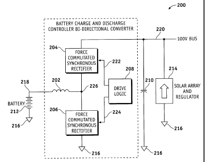
Figure 2 is an illustration of an exemplary synchronous rectifier bi-
directional
converter system 200 according to an embodiment of the disclosure. The
synchronous rectifier bi-directional converter system 200 comprises an
inductor
202, a first force commutated synchronous rectifier 204, a second force
commutated synchronous rectifier 206,drive logic 208, a boost side capacitor
210,
a battery 212, and a solar array 214.Figure 2 shows a partial schematic of a
power stage for the synchronous rectifier bi-directional converter system 200
operating as a battery charge/discharge regulator.
The inductor 202 is coupled to the first force commutated synchronous
rectifier
204 and the second force commutated synchronous rectifier 206 via an
electrical
bus 226, and is coupled to the battery 212 via a link 218. The first force
commutated synchronous rectifier 204 is coupled to the drive logic 208 via a
link
222, and the second force commutated synchronous rectifier 206 is coupled to
the
drive logic 208 via a link 224. The boost side capacitor 210 is coupled to the
solar
- 14-
CA 02756180 2011-10-24
array 214 and the first force commutated synchronous rectifier 204 via the
electrical bus 220. The battery 212, the second force commutated synchronous
rectifier 206, the boost side capacitor 210, and the solar array 214 are each
connected to the common ground 216 respectively.
In a spacecraft application, a voltage of an electrical bus220 is higher than
a
voltage of the battery 212. Therefore, when the solar array 214 is producing
insufficient power to meet the spacecraft needs, the synchronous rectifier bi-
directional converter system 200 draws power from the battery212 to provide a
necessary current for the electrical bus220. When the solar array 214 has
excess
power available, the synchronous rectifier bi-directional converter system 200
becomes a buck regulator to charge the battery 212. Therefore, since current
must flow out of the battery212 to power the electrical bus220 and into the
battery
212 to charge the battery212, the synchronous rectifier bi-directional
converter
system 200 is a bi-directional power processor. Furthermore, since the
switching
rectifiers are FETs that are turned on at the appropriate times, the
synchronous
rectifier bi-directional converter system 200 is synchronous rectified.
Since the voltage drop of a FET is generally much lower than the voltage drop
of a
rectifier, the synchronous rectifier bi-directional converter system 200can
achieve
much higher efficiency than a conventional buck or boost regulator. That is,
when
boosting from an 80V battery to a 100V electrical bus, an existing boost
regulator
will have an efficiency of approximately 96.5%. The synchronous rectifier bi-
directional converter system 200may have an efficiency of approximately 98%.
This efficiency improvement is a result of reduced rectifier losses and
reduced
-15-
CA 02756180 2011-10-24
switching losses associated for the synchronous rectifier bi-directional
converter
system 200.
Figure 3 is an illustration of an exemplary synchronous rectifier bi-
directional
converter system 300 according to an embodiment of the disclosure. The
synchronous rectifier bi-directional converter system 300 comprises an
inductor
302 (202 in Figure 2), a first force commutated synchronous rectifier 304 (204
in
Figure 2) a second force commutated synchronous rectifier 306 (206 in Figure
2),
drive logic 308 (208 in Figure 2), a reaction wheel 310, and a spacecraft
load314.
Figure 3 shows a partial schematic of a power stage for the synchronous
rectifier
bi-directional converter system 300 operating as a 30V electrical bus318
regulator.
The inductor 302 is coupled to the first force commutated synchronous
rectifier
304 and the second force commutated synchronous rectifier 306 via an
electrical
bus 326, and is coupled to the reaction wheel 310, and the spacecraft load314
via
the 30V electrical bus 318. The first force commutated synchronous rectifier
304
is coupled to the drive logic 308 via a link 322, and the second force
commutated
synchronous rectifier 306 is coupled to the drive logic 308 via a link 324.
The
reaction wheel 310, the spacecraft load314, and the second force commutated
synchronous rectifier 306, are each connected to the common ground 316
respectively.
The synchronous rectifier bi-directional converter system 300functions as a
buck
regulator to transform a 100V electrical bus 320 operating at 100V to the 30V
-16-
CA 02756180 2013-09-25
electrical bus 318. In some cases, an energy from the reaction wheel 310 may
be
dumped back into the 30 Velectrical bus 318 in such a way that power dumped
from the reaction wheel 310 exceeds the 30V electrical bus 318 for the
spacecraft
load 314. In this case, the synchronous rectifier bi-directional converter
system
300 operates as a boost shunt regulator to return excess power to the 100V
electrical bus320 where there is substantially always sufficient spacecraft
load to
absorb the power.
Figure 4 is an illustration of an exemplary synchronous rectifier bi-
directional
converter system 400 according to an embodiment of the disclosure. The
synchronous rectifier bi-directional converter system 400 comprises an
inductor
L1 coupled to battery V1 and a resistor R3, a first force commutated
synchronous
rectifier 404 (similar to 304 in Figure 3), and a second force commutated
synchronous rectifier 406 (similar to 306 in Figure 3).
Figure 4 shows a SPICE model of the synchronous rectifier bi-directional
converter system 400 (system 400) configured to operate as a battery charge /
discharge regulator. As shown
in Figure 4, the first force commutated
synchronous rectifier 404 comprises a high side forced commutation circuit 410
(U7)and a high side driver 408 (U3) coupled to a transformer TX1. The
transformer TX1 comprises a primary P1 and a secondary S1, and a resistor R1
and may be coupled to a capacitor Cl and a bus 402 (U2). Similarly, the first
force commutated synchronous rectifier 406 comprises a low side forced
commutation circuit 414 (U6) and a low side driver 412 (U5) coupled to a
transformer TX2. The transformer TX2 comprises a primary P1 and a secondary
S1, and a resistor R2.
- 17-
CA 02756180 2011-10-24
A high side FET (or switch) Q1 and a low side FET (or switch) Q2are the
synchronous switches that either connect VL (right side of the inductor) to an
output or ground respectively. The high side forced commutation circuit 410
(U7)
and the low side forced commutation circuit 414(U6) prevent body diode
conduction in the high side FET Q1 and in the low side FET 02 respectively.
The
high side forced commutation circuit 410 and the low side forced commutation
circuit 414processa pulse-width modulation (PWM) signal (DR1) to create drive
signals for the low side FET Q2and the high side FETQ1 respectively. The low
side FET Q2 is driven by a signal that is substantially in phase with the PWM
signal (DR1). The high side driver 408 (U3) drives the high side FET Q1 with a
signal that is essentially an inverted version of the DR1.
In addition to driving the low side FET Q2, the low side driver 412 (U5)
delays the
arrival of the gate drive signal so that the high side FET Q1 has time to turn
off
before the low side FET Q2turns on. Similarly, the low side forced commutation
circuit 414 delays the turn-on of high side FET Qlso that the low side FET
Q2has
sufficient time to turn off before the high side FET Q1turns on.
The PWM signal from a PWM control circuit (not shown) uses voltage and current
feedback to regulate the electrical bus voltage by adjusting pulse a width of
the
DR1. As DR1 duty cycle increases, the output electrical bus voltage increases.
As the DR1 duty cycle decreases, the electrical bus voltage decreases.
When the system 400 is functioning as a boost converter to supply current to
the
100Velectrical bus, the low side FET Q2 has current flowing from a drain to a
- 18-
CA 02756180 2011-10-24
source of the low FET Q2 and is therefore shown as positive current into the
low
side FET 02. Since the current flow from the drain to the source of the low
FET
02, there is no chance that the body diode of the low side FET 02 will have
current flowing in it when the low side FET Q2is turned off. Therefore,
although
the low side forced commutation circuits 414 is attached and operating, it
does not
perform a useful function for a boost converter operating mode.
The high side FET Q1 current flows from to a source to a drain of the FET Q1.
Therefore at turn-off, it is essential for the high side forced commutation
circuit
410 to reverse the current in the FET before the device is turned off to
prevent
body diode conduction. When the high side forced commutation circuit 410 is
activated, the current reverses in the FET followed by the turn-off of the
high side
FET Q1. Then, a current of the inductor L1continues to flow in the high side
forced commutation circuit 410until the low side FET Q21s turned on.
When the system 400 is functioning as a buck converter to charge the battery,
the
high side FET Q1 has current flowing from drain to source and is therefore
shown
as positive current into the high side FET Q1. Since the current flow from
drain to
source, there is no chance that the body diode of the high side FET Q1will
have
current flowing in it when the high side FET Q1is turned off. Therefore,
although
the high side forced commutation circuit 410 is attached and operating, it
does not
perform a useful function for the buck converter operating mode.
The low side FET Q1 current flows from to source to drain (e.g., as can be
indicated by negative current). Therefore at turn-off, it is essential for the
forced
- 19-
CA 02756180 2011-10-24
commutation circuit to reverse the current in the low side FET Q1before the
device is turned off to prevent body diode conduction. When the commutation
circuit 410 is activated, the current reverses in the low side FET Q1followed
by the
turn-off of the high side FET Q1. Then, a current in the inductor L1continues
to
flow in the commutation circuit 410 until the low side FET Q2is turned on.
In summary, two forced commutation circuits are required to efficiently
operate a
synchronous rectified bi-directional converter: (1) the
high side forced
commutation circuit 410 in parallel with the high side FETQ1 is necessary to
avoid
losses associated with the reverse recovery characteristics of the high side
FET
01 when the system 400 operates as a boost converter to regulate the
electrical
bus, and (2) the low side forced commutation circuit 414 in parallel with the
low
side switch Q2 is necessary to avoid losses associated with the reverse
recovery
characteristics of the high side FET Q1when the synchronous rectifier bi-
directional converter system 400 operates as a boost converter to regulate the
electrical bus.
Although this principal is illustrated using a boost/buck regulator, it can be
applied
to other converters such as, for example but without limitation, a buck-boost
(inverting flyback) converter, a non-inverting flyback, a Cuk converter, or a
coupled inductor buck converter. A basic principal described herein is that
two (or
more) forced commutation circuits can be used to convert nearly any switching
regulator into a synchronous rectified bi-directional converter.
- 20 -
CA 02756180 2011-10-24
Figure 5 is an illustration of an exemplary flowchart showing a bi-directional
voltage conversion process 500 (process 500) according to an embodiment of the
disclosure. The various tasks performed in connection with process 500 may be
performed mechanically, by software, hardware, firmware, or any combination
thereof. It should be appreciated that the process500 may include any number
of
additional or alternative tasks, the tasks shown in Figure 5 need not be
performed
in the illustrated order, and the process 500 may be incorporated into a more
comprehensive procedure or process having additional functionality not
described
in detail herein.
For illustrative purposes, the following description of the process 500 may
refer to
elements mentioned above in connection with Figures 1-4. In
practical
embodiments, portions of the process 500 may be performed by different
elements of the systems100-400 such as: the source terminal 112, the gate
terminal 114, the drain terminal 116, the intrinsic body diode 118, the
inductor
302/L1, the first force commutated synchronous rectifier304/404, the second
force
commutated synchronous rectifier306/406, etc. The process 500 may have
functions, material, and structures that are similar to the embodiments shown
in
Figures 1-4. Therefore common features, functions, and elements may not be
redundantly described here.
Process 500 may begin by receiving a charge current at a first voltage on the
first
force commutated synchronous rectifier 304/404(task 502).
- 21 -
CA 02756180 2011-10-24
Process 500 may continue by controlling the charge current with the first
force
commutated synchronous rectifier 304/404(task 504).
Process 500 may continue by charging the inductor 302/L1with the charge
current
(task 506).
Process 500 may continue by controlling a discharge current from the inductor
302/L1 using the second force commutated synchronous rectifier306/406(task
508).
Figure 6 is an illustration of an exemplary flowchart showing a process 600
for
using a bi-directional voltage conversion system according to an embodiment of
the disclosure. The various tasks performed in connection with the process 600
may be performed mechanically, by software, hardware, firmware, or any
combination thereof. It should be appreciated that the process600 may include
any number of additional or alternative tasks, the tasks shown in Figure 6
need
not be performed in the illustrated order, and the process 600 may be
incorporated into a more comprehensive procedure or process having additional
functionality not described in detail herein.
For illustrative purposes, the following description of the process 600 may
refer to
elements mentioned above in connection with Figures 1-4. In
practical
embodiments, portions of the process 600 may be performed by different
elements of the systems100-400such as: the source terminal 112, the gate
terminal 114, the drain terminal 116, the intrinsic body diode 118, the
inductor
- 22 -
CA 02756180 2011-10-24
302/L1, the first force commutated synchronous rectifier304/404, the second
force
commutated synchronous rectifier306/406, etc. The process 600 may have
functions, material, and structures that are similar to the embodiments shown
in
Figures 1-4. Therefore common features, functions, and elements may not be
redundantly described here.
Process 600 may begin by receiving a first current at a first voltage (task
602).
Process 600 may continue by controlling flow of the first current into the
inductor
302/L1with the first force commutated synchronous rectifier 304/404coupled to
the
inductor 302/L1 (task 604).
Process 600 may continue by controlling flow of a second current from the
inductor 302/L1with the second force commutated synchronous rectifier
306/406coupled to the inductor 302/L1and the first force commutated
synchronous rectifier 304/404 (task 606).
Process 600 may continue by regulating a second voltage at an output of the
inductor 302/L1 (task 608).
In this way, embodiments of the disclosure provide two forced commutation
synchronous rectifiers can be used in such a way that a converter can
efficiently
process power in two directions. The forced commutation method is more
efficient. Since no series diode is required when using the force commutated
switch, the efficiency improves dramatically since typically the FET losses
are
- 23 -
CA 02756180 2011-10-24
much lower than the rectifier losses. Lower power dissipation reduces the
weight
of the power devices since less heat sink material is required and components
may be packaged more densely. In this manner, spacecraft weight can be
reduced since less thermal management hardware is required.
By using the synchronous rectifier bi-directional converter described herein,
power
can flow either from the AC electrical bus to the DC electrical bus or from
the DC
electrical bus to the AC electrical bus.
The above description refers to elements or nodes or features being
"connected"
or "coupled" together. As used herein, unless expressly stated otherwise,
"connected" means that one element/node/feature is directly joined to (or
directly
communicates with) another element/node/feature, and not necessarily
mechanically. Likewise, unless expressly stated otherwise, "coupled" means
that
one element/node/feature is directly or indirectly joined to (or directly or
indirectly
communicates with) another element/node/feature, and not necessarily
mechanically. Thus,
although Figures1-4 depict example arrangements of
elements, additional intervening elements, devices, features, or components
may
be present in an embodiment of the disclosure.
Terms and phrases used in this document, and variations thereof, unless
otherwise expressly stated, should be construed as open ended as opposed to
limiting. As examples of the foregoing: the term "including" should be read as
mean "including, without limitation" or the like; the term "example" is used
to
provide exemplary instances of the item in discussion, not an exhaustive or
-24 -
CA 02756180 2011-10-24
limiting list thereof; and adjectives such as "conventional," "traditional,"
"normal,"
"standard," "known" and terms of similar meaning should not be construed as
limiting the item described to a given time period or to an item available as
of a
given time, but instead should be read to encompass conventional, traditional,
normal, or standard technologies that may be available or known now or at any
time in the future.
Likewise, a group of items linked with the conjunction "and" should not be
read as
requiring that each and every one of those items be present in the grouping,
but
rather should be read as "and/or" unless expressly stated otherwise.
Similarly, a
group of items linked with the conjunction "or" should not be read as
requiring
mutual exclusivity among that group, but rather should also be read as
"and/or"
unless expressly stated otherwise. Furthermore, although items, elements or
components of the disclosure may be described or claimed in the singular, the
plural is contemplated to be within the scope thereof unless limitation to the
singular is explicitly stated. The presence of broadening words and phrases
such
as "one or more," "at least," "but not limited to" or other like phrases in
some
instances shall not be read to mean that the narrower case is intended or
required
in instances where such broadening phrases may be absent.
- 25 -