Note: Descriptions are shown in the official language in which they were submitted.
1
Title of the Invention:
Radiographic image detector
Technical Field:
[0001]
This invention relates to a novel radiographic image
detector. The radiographic image detector can be used
preferably in medical fields such as positron emission tomography
and X-ray CT, industrial fields such as various nondestructive
tests, and security fields such as radiation monitors and
inspection of personal belongings.
Background Art:
[0002]
Radiation application technologies (i.e., technologies
utilizing radiation) cover a wide range of fields, including
medical fields such as positron emission tomography and X-ray
CT, industrial fields such as various nondestructive tests, and
security fields such as radiation monitors and inspection of
personal belongings, and are making marked progress even now.
Radiographic image detectors are constituent
technologies occupying an important position in the radiation
application technologies. With the progress of the radiation
application technologies, the radiographic image detectors are
required to achieve higher performance in connection with
detection sensitivity, position resolution on the incident
position of radiation, or count rate characteristic. As the
radiation application technologies find widespread use, cost
reduction and an increased sensitive volume are also demanded
of the radiographic image detectors.
[0003]
To fulfill the above demands made on the radiographic
image detectors, a particle beam image detector using gas
multiplication (maybe called amplification) bya pixel electrode
has been developed (see Patent Document 1) . The particle beam
2
image detector allows an incident particle beam to ionize gas
molecules, thereby producing electrons, and detects the
electrons by the pixel electrode. The particle beam image
detector is advantageous in that it is excellent in position
resolution and count rate characteristic, can easily increase
the sensitive volume, and can be manufactured inexpensively.
However, the gas used therein has a low atomic weight, and thus
shows low stopping power against photons having high energy,
such as hard X-rays and gamma rays. The particle beam image
detector, therefore, posed the problem of low detection
sensitivity to these photons.
[0004]
In the light of such problems, the present inventors
have already proposed a method comprising converting incident
radiation into ultraviolet rays with the use of a scintillator
composed of a chemical substance having a large atomic weight,
and detecting the ultraviolet rays by a gas multiplication
detector having position resolution (see Patent Document 2).
An attempt to detect radiation by a similar method has also been
made by other people (see Non-Patent Document 1) . With these
methods, however, the ultraviolet rays produced by the
scintillator ionize gas molecules to generate electrons, and
the resulting electrons are detected. Thus, the range (i.e.,
the travel distance before energy loss) of the ultraviolet rays
covers an extent corresponding to the thickness of a gas layer.
Consequently, such detectors, when used as radiographic image
detectors, have posed the problem of declining in position
resolution and count rate characteristic. Since chemically
unstable gas molecules need to be used, moreover, the problem
has occurred that the gas molecules themselves deteriorate, or
the gas molecules deposit on the electrode of the detector. These
problems have posed difficulty in operating the detectors stably
for a long term (see Non-Patent Document 2).
[0005]
Another attempt has been made at a method for detecting
3
ultraviolet rays produced from radiation by a scintillator, the
method comprising converting the ultraviolet rays into electrons
with the use of a photoelectric conversion substance, and
detecting the electrons by a gas multiplication detector (see
Non-Patent Document 3). According to this method, the
above-mentioned decreases in position resolution and count rate
characteristic and the problem about the stability of operation
are considered to be avoidable, but it has been unsuccessful
to sufficiently increase a multiplication factor in multiplying
or amplifying the electrons by the gas multiplication detector.
As a result, very feeble ultraviolet rays generated from the
scintillator have not been detectable with satisfactory
sensitivity. To date, there have been no attempts to prepare
an apparatus which can detect a radiographic image by such a
method using a photoelectric conversion substance.
Prior Art Documents:
Patent Documents:
[0006]
Patent Document 1: Japanese Patent No. 3354551
Patent Document 2: JP-A-2008-202977
Non-Patent Documents:
[0007]
Non-Patent Document 1: P. Schotanus, et al., "Detection of
LaF3:Nd3+ Scintillation Light in a Photosensitive Mutiwire
Chamber" Nuclear Instruments and Methods in Physics Research,
A272, 913-916 (1988).
Non-Patent Document 2: J. Va'vra, "Wire Aging of Hydrocarbon
Gases with TMAE Additions" IEEE Transactions on Nuclear Science,
NS-34, 486-490 (1987).
Non-Patent Document 3: J. van der Marel, et al., "A LaF3:Nd
(10%) Scintillation Detector with Microgap Gas Chamber Read-out
for the Detection of y-rays" Nuclear Instruments and Methods
in Physics Research, A392, 310-314 (1997).
4
Summary of the Invention:
Problems to be solved by the invention:
[0008]
It is an object of the present invention to provide a
radiographic image detector which can detect radiation, such
as hard X-rays or y-rays, with high sensitivity and which is
excellent in position resolution and count rate characteristic,
the radiographic image detector being composed of a combination
of a scintillator for converting incident radiation into
ultraviolet rays, and a novel gas multiplication ultraviolet
image detector for converting ultraviolet rays into electrons,
amplifying such electrons, and detecting the amplified
electrons.
Means for solving the problems:
[0009]
The present inventors have paid attention to a gas
multiplication ultraviolet image detector constituting a
radiographic image detector, and conducted extensive studies
on a method for detecting very feeble ultraviolet rays, which
are produced by a scintillator, with satisfactory sensitivity.
As a result, they have found that using a gas
multiplication ultraviolet image detector composed of a
photoelectric conversion substance, a gas electron multiplier,
and a pixel electrode, ultraviolet rays produced by a
scintillator are converted into electrons by the photoelectric
conversion substance, and then the electrons are amplified by
the gas electron multiplier, and then the amplified electrons
are detected with the use of the pixel electrode, whereby
radiation can be detected with satisfactory sensitivity. They
have also succeeded in obtaining a radiographic image by a
radiographic image detector comprising a combination of the
scintillator and the gas multiplication ultraviolet image
detector. This success has led them to accomplish the present
invention.
5
That is, according to the present invention, there is
provided a radiographic image detector including a scintillator
for converting incident radiation into ultraviolet rays, and
a gas multiplication ultraviolet image detector, wherein the
gas multiplication ultraviolet image detector is composed of
a photoelectric conversion substance,a gas electron multiplier,
and a pixel electrode.
In the above invention of the radiographic image detector,
it is preferred that
(1) the scintillator be a metal fluoride crystal
containing neodymium, praseodymium, thulium or erbium;
(2) the photoelectric conversion substance be cesium
iodide or cesium telluride; and
(3) two or three of the gas electron multipliers be
present.
Effects of the invention:
[0010].
According to the present invention, extremely feeble
ultraviolet rays produced upon conversion from radiation by the
scintillator can be detected with high sensitivity. Thus, a
radiographic image detector excellent in position resolution
and count rate characteristic can be provided. Moreover, the
radiographic image detector of the present invention can easily
upsize the sensitive volume, and can be manufactured at a low
cost. Hence, the radiographic image detector of the present
invention is of immense value in the fields of medicine, industry,
security, etc.
Brief Description of the Drawings:
[0011]
[Fig. 1] is a schematic view of a radiographic image detector
according to the present invention.
[Fig. 2] is a schematic view of a radiographic image detector
according to the present invention.
6
[Fig. 3] is a schematic view of a radiographic image detector
according to the present invention.
[Fig. 4] is a schematic view of a radiographic image detector
according to the present invention.
[Fig. 5] shows schematic views of a gas electron multiplier used
in the present invention.
[Fig. 6] is a radiographic image obtained in Example 1.
[Fig. 7] is a radiographic image obtained in Example 2.
[Fig. 8] is a radiographic image obtained in Example 3.
[Fig. 9] is a radiographic image obtained in Example 3.
[Fig. 10] is a radiographic image obtained in Example 3.
[Fig. 11] shows the profiles of radiation detection frequencies
in the radiographic images obtained in Example 3.
Mode for Carrying Out the Invention:
[0012]
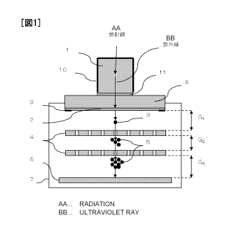
[Operating principle]
The operating principle of the radiographic image
detector according to the present invention will be described
using Fig. 1. First, incident radiation is converted into
ultraviolet rays by a scintillator 1. Then, the resulting
ultraviolet rays are converted into primary electrons 3 by a
photoelectric conversion substance 2. The primary electrons
3 are amplified by gas electron multipliers 4, which utilize
a multiplication effect due to a gas electron avalanche
phenomenon in a high electric field, to obtain secondary
electrons 5. Then, the secondary electrons 5 are further
amplified and detected by a pixel electrode 6. Signals based
on the electrons detected by the pixel electrode are processed
by an external circuit, whereby the position of incidence of
the radiation can be identified to obtain a radiographic image.
The radiographic image detector of the present invention will
be described in more detail below.
[0013]
[Scintillator]
7
As the scintillator which is a constituent element of
the radiographic image detector of the present invention, any
scintillator producing ultraviolet rays upon entry of radiation
can be used without limitation. In the light of the efficiency
of photoelectric conversion from ultravioletraysinto electrons
in the photoelectric conversion substance, however, it is
particularly preferred to use a scintillator which produces
vacuum ultraviolet rays with a wavelength of 200 nm or less among
ultraviolet rays.
By selecting the scintillator used, in accordance with
the type of radiation to be detected, any radiation such as X-rays,
a-rays, (3-rays, y-rays or neutron beam becomes detectable.
In particular, the scintillator comprising a chemical substance
having a high atomic weight is preferred, because it can
efficiently detect photons of high energy, such as hard X-rays
or y -rays, among radiations.
In order to allow the ultraviolet rays, produced by the
entry of radiation, to exit without being absorbed by the
scintillator itself, it is preferred to use a scintillator which
minimally absorbs ultraviolet rays. Examples of such a
scintillator minimally absorbing ultraviolet rays include
scintillators composed of metal fluorides to be described later;
metal oxides such as alumina (A1203) , yttrium aluminate (YA103)
and lutetium aluminate (Lu3A15O12); metal phosphates such as
lutetium phosphate (LuPO4) and yttrium phosphate (YPO4) ; or some
metal borates.
The forms of these scintillators are not limited, and
any forms such as crystal, glass and ceramic can be used as
appropriate. From the viewpoint of the efficiency of conversion
from radiation into ultraviolet rays, the use of a crystal is
preferred.
[0014]
As the scintillator which produces the vacuum ultraviolet
rays, the metal fluoride can be used preferably. Since vacuum
ultraviolet rays have the property of being absorbed by many
8
materials, the problem occurs that vacuum ultraviolet rays
generated by the entry of radiation are absorbed by the
scintillator itself. However, the metal fluoride, as an
exception, has the property of minimally absorbing vacuum
ultraviolet rays, and thus can be used preferably in the present
invention.
The type of the metal fluoride is not limited, and any
publicly known metal fluorides can be used as the scintillator
producing vacuum ultraviolet rays. Concretely, the following
metal fluorides are named as examples: lithium fluoride,
magnesium fluoride, calcium fluoride, scandium fluoride,
titanium fluoride, chromium fluoride, manganese fluoride, iron
fluoride, cobalt fluoride, nickel fluoride, copper fluoride,
zinc fluoride, gallium fluoride, germanium fluoride, aluminum
fluoride, strontium fluoride, yttrium fluoride, zirconium
fluoride, barium fluoride, lanthanum fluoride, cerium fluoride,
praseodymium fluoride, neodymium fluoride, europium fluoride,
gadolinium fluoride, terbium fluoride, erbium fluoride, thulium
fluoride, ytterbium fluoride, lutetium fluoride, hafnium
fluoride, tantalum fluoride, and lead fluoride.
[0015]
In the present invention, it is preferred that compounds
containing luminescence center elements, which generate
radiative transition in the ultraviolet region, be used as the
scintillator. Any luminescence center elements may be used
without limitation, as long as they show emission of ultraviolet
rays by radiative transition. The luminescence center elements,
which exhibit 5d-4f transition light emission due to electron
transition f rom 5d level to 4 f level, are particularly preferred,
because they have a short light emission lifetime and a fast
response. As such luminescence center elements exhibiting
5d-4f transition light emission, praseodymium (Pr), neodymium
(Nd), erbium (Er) and thulium (Tm) can be used preferably.
[0016]
In the scintillator containing the luminescence center
9
element, the content of the luminescence center element varies
according to the type of the scintillator or the type of the
luminescence center element, but usually, a content in the range
of 0. 005 to 20 wt. % is preferred. By setting the amount of the
luminescence center element added at 0.005 wt.% or more, the
intensity of light emission of the scintillator can be enhanced.
By setting this amount at 20 wt. % or less, on the other hand,
attenuation of light emission by the scintillator ascribed to
concentration quenching can be suppressed.
The preferred scintillator containing the luminescence
center element is exemplified by crystals comprising the
aforementioned metal fluorides, metal oxides, or metal
phosphates, the crystals containing the luminescence center
element exhibiting the aforesaid 5d-4f transition light
emission.
[0017]
In the present invention, it is preferred to use the
scintillator comprising a chemical substance having a high
density and a high effective atomic number, in order to enhance
the detection sensitivity to photons of high energy, such as
hard X-rays or y -rays. The effective atomic number is an
indicator defined by the equation [1] shown below, and affects
the stopping power against hard X-rays or y -rays. The higher
the effective atomic number is, the greater the stopping power
against hard X-rays or -y-rays becomes. As a result, the
sensitivity of the scintillator to hard X-rays or y-rays
increases.
Effective atomic number = ( EWiZi4) 114 [1]
where Wi and Zi denote, respectively, the mass fraction and atomic
number of the i-th element of the elements constituting the
scintillator.
[0018]
The shape of the scintillator is not limited. Preferably,
however, the scintillator has an ultraviolet emergence surface
opposing a gas multiplication ultraviolet image detector to be
10
described later (may hereinafter be referred to simply as an
ultraviolet emergence surface), and the ultraviolet emergence
surface has been optically polished. By providing such an
ultraviolet emergence surface, ultraviolet rays produced by the
scintillator can be efficiently entered into the gas
multiplication ultraviolet image detector.
The shape of the ultraviolet emergence surface is not
limited, and shapes conformed to uses can be suitably selected,
such as a square shape several millimeters to several hundred
millimeters square, and a circular shape of several millimeters
to several hundred millimeters in diameter. The thickness, in
the direction of incidence of radiation, of the scintillator
varies with the type and energy of the radiation to be detected,
but generally, is several hundred micrometers to several hundred
millimeters.
Application of an ultraviolet reflective coating or film,
which comprises aluminum or Teflon, to a surface not opposing
the gas multiplication ultraviolet image detector is preferred,
because dissipation of ultraviolet rays produced by the
scintillator can be prevented. By using an array of many of
the scintillators coated with the ultraviolet reflective film,
moreover, the position resolution of the radiographic image
detector can be enhanced remarkably.
[0019]
The method for manufacturing the scintillator is not
limited, and the scintillator can be manufactured by a publicly
known manufacturing method. In manufacturing a metal fluoride
crystal which is the preferred scintillator in the present
invention, it is preferred to manufacture it by the melt growth
method such as Czochralski method or Bridgman method.
Manufacture by the melt growth method enables a metal fluoride
crystal excellent in quality, such as transparency, to be
produced. Moreover, a large crystal having a diameter of several
inches can be produced at a low cost.
In order to eliminate a crystal defect due to thermal
11
strain or the like in the manufacture of the metal fluoride crystal,
annealing may be performed after the manufacture of the crystal.
The resulting metal fluoride crystal has satisfactory
processability and, after being processed into a desired shape,
is used as a scintillator. For its processing, a cutter such
as a blade saw or a wire saw, a grinder or an abrasive wheel,
which is publicly known, can be used without limitation.
{0020]
The gas multiplication ultraviolet image detector
included in the radiographic image detector of the present
invention is basically constituted by a photoelectric conversion
substance, a gas electron multiplier, and a pixel electrode.
The gas multiplication ultraviolet image detector will be
described concretely below.
[0021]
[Photoelectric conversion substance]
The photoelectric conversion substance functions to
convert ultraviolet rays, which have been produced by the
scintillator, into primary electrons. The photoelectric
conversion substance is not limited in type, if it has the above
function. Concretely, cesium iodide (CsI) and cesium telluride
(CsTe) can be named as examples. Of them, cesium iodide is
preferred from the viewpoint of the efficiency of photoelectric
conversion in converting ultraviolet rays into electrons, and
the viewpoint of chemical stability.
The photoelectric conversion substance is preferably
in the form of a thin film for the purpose of efficient withdrawal
of primary electrons converted from ultraviolet rays. As will
be described later, moreover, it is preferred that the
photoelectric conversion substance thin film be formed on the
inner surface of an ultraviolet entrance window, or be formed
on a surface of the gas electron multiplier opposing the
ultraviolet entrance window.
[0022]
[Gas electron multiplier]
12
Then, the primary electrons produced by the photoelectric
conversion substance are amplified by a gas electron multiplier.
The gas electron multiplier was developed by Sauli in 1997, and
is known as GEM. In the present invention, the technology
described, forexample,in JP-A-2006-302844orJP-A-2007-234485
can be used preferably as the gas electron multiplier.
Hereinbelow, the gas electron multiplier used in the present
invention will be described in detail with the use of Fig. 5.
The gas electron multiplier is composed of a plate-shaped
multilayer body constituted by a plate-shaped insulating layer
12 formed from resin, and planar metal layers 13 coated on both
surfaces of the plate-shaped insulating layer; and through-holes
14 provided in the plate-shaped multilayer body and each having
an inner wall perpendicular to the flat surfaces of the metal
layers. In the gas electron multiplier, a predetermined applied
voltage is applied to the metal layers to generate an electric
field inside the through-holes. By so doing, the primary
electrons entering the interior of the through-hole structure
are accelerated to cause an electron avalanche phenomenon, and
they are amplified to become many secondary electrons while
retaining position information. The material for the
plate-shaped insulating layer is preferably a polyimide, a liquid
crystal polymer or the like in view of the processability and
mechanical strength.
[0023]
The larger the thickness (Di in Fig. 5) of the plate-shaped
insulating layer, the more effectively discharge between the
metal layers on the face and back of the gas electron multiplier
can be suppressed. Thus, a higher applied voltage is applied,
whereby an increased multiplication factor can be obtained. If
the thickness is excessively large, however, processing for
providing the through-holes is difficult. Thus, the thickness
of the plate-shaped insulating layer is preferably set at 50
pm to 300 pm. The material for and thickness (Dm in Fig. 5)
of the metal layer are not limited. For example, however, the
13
preferred metal layer is one whose material is copper, aluminum
or gold, and whose thickness is of the order of 5 gm.
The diameter (d in Fig. 5) of the through-hole is not
limited, and selected, as appropriate, in consideration of the
strength of an electric field generated within the through-hole,
the ease of processing, etc. A concrete example of such a
diameter is generally 50 to 100 gm. The through-holes are
preferably provided at a predetermined pitch (P in Fig. 5) in
the entire plate-shaped multilayer body in order to enhance the
uniformity of the electric field generated. This pitch depends
on the material for and thickness of the plate-shaped insulating
layer and the diameter of the through-hole, but is generally
about twice the diameter of the through-hole. In providing the
through-holes, they are preferably disposed in an.arrangement
of regular triangles, as shown in Fig. 5. By adopting such an
arrangement, the open area ratio of the through-holes to the
area of the plate-shaped multilayer body can be increased. Thus,
a high multiplication factor can be obtained, and an ion feedback
to be described later can be suppressed.
[0024]
In the operation of the gas electron multiplier, the
higher the applied voltage is, the higher multiplication factor
is obtained. If the applied voltage is extremely high, however,
discharge occurs between the metal layers on the face and back
of the gas electron multiplier, making a stable operation
difficult. The preferred range of the applied voltage varies
with the thickness of the plate-shaped insulating layer, but
isgenerally 200Vto1,000V. The multiplication factor obtained
at such an applied voltage is generally several tens to several
thousands.
[0025]
[Pixel electrode]
Secondary electrons amplified by the gas electron
multiplier are further amplified and detected using a pixel
electrode. The pixel electrode is disclosed in detail in the
14
aforementioned Patent Document 1, and thus may be prepared in
accordance with the technology disclosed therein.
Concretely, the pixel electrode includes anode strips
formed on the back ofa double-sided substrate, cylindrical anode
electrodes planted in the anode strips and each having an upper
end surface exposed at the face of the double-sided substrate,
and strip-shaped cathode electrodes each having holes formed
around the upper end surf aces of the cylindrical anode electrodes.
The anode strips each preferably have a width of 200 um to 400
gm. Particularly preferably, the anode strips are arranged
at intervals of 400 t Lm, the strip-shaped cathode electrodes
each have the holes with a diameter of 200 to 300 gm formed
at constant intervals, and the cylindrical anode electrodes each
have a diameter of 40 to 60 um and a height of 50 to 150 u
m.
[0026]
By applying a predetermined applied voltage between the
cylindrical anode electrode and the strip-shaped cathode
electrode of the pixel electrode, a strong electric field occurs
in the vicinity of the cylindrical anode electrode. Secondary
electrons accelerated by this electric field undergo an electron
avalanche and, after being amplified, they are detected by the
cylindrical anode electrode. Gas molecules cationized during
this process rapidly drift to the surrounding strip-shaped
cathode electrode. Thus, electric charges observable on the
electric circuit are produced in both of the cylindrical anode
electrode and the strip-shaped cathode electrode. Observation
of which strip of the anodes and the cathodes the multiplication
phenomenon has occurred in, therefore, tells the position of
the incident particle beam. As a signal processing circuit for
reading out signals and obtaining a two-dimensional image, a
publicly known one can be used without limitation.
[0027]
The preferred range of the applied voltage of the pixel
electrode varies according to the type of the gas used, but is
15
generally 400V to 800V. The pixel electrode uses pixels as the
anodes, and thus easily createsa high electric field, resulting
in a high multiplication factor. Hence, the multiplication
factor obtained at the above applied voltage reaches a value
as great as several thousands to several tens of thousands. With
the pixel electrode, moreover, the distance over which the
cationized gas molecules drift is extremely short. Compared
with other gas multiplication detectors, therefore, the pixel
electrode has a short dead time, and has a high count rate
characteristic exceeding about 5X 10⁶ counts/ (sec = mm2) .
Furthermore, the pixel electrode can be produced using a
technology for preparing a printed circuit board, so that the
pixel electrode having a large area can be provided at a low
cost.
[0028]
[Gas multiplication ultraviolet image detector]
A preferred mode for constituting a gas multiplication
ultraviolet image detector using the photoelectric conversion
substance, gas electron multiplier, and pixel electrode
described above will be described in detail with the use of Fig.
1.
Within a chamber 7 having an opening for admitting
ultraviolet rays produced by the scintillator 1, the
photoelectric conversion substance 2, the gas electron
multiplier 4, and the pixel electrode 6 are installed in this
sequence, starting on the side nearer the opening, and the opening
is sealed with an ultraviolet entrance window 8. As a material
for the ultraviolet entrance window, it is preferred to use
lithium fluoride (LiF), magnesium fluoride (MgF2) or calcium
fluoride (CaF2) which is highly pervious to ultraviolet rays.
The interior of the chamber is filled with a predetermined
gas. A combination of a rare gas and a quencher gas is generally
used as this gas for electron multiplication. Examples of the
rare gas are helium (He) , neon (Ne) , argon (Ar) and xenon (Xe) .
Examples of the quencher gas are carbon dioxide (CO2) , methane
= 16
(CHO) , ethane (C2H6), and tetrafluoromethane (CF4) . The amount
of the quencher gas mixed into the rare gas is preferably 5 to
300.
[0029]
The photoelectric conversion substance preferably
assumes the form of a thin film in order to efficiently withdraw
primary electrons converted from ultraviolet rays. This thin
film is preferably formed on the inner surface of the ultraviolet
entrance window as shown in Fig. 1, or formed on a surface of
the gas electron multiplier opposing the ultraviolet entrance
window as shown in Fig. 2.
In forming the thin film of the photoelectric conversion
substance on the inner surf ace of the ultraviolet entrance window,
it is preferred to provide an electrode 9, which comprises a
metal layer, in an outer peripheral portion on the thin film,
in order to supply electrons efficiently to the thin film, and
in order to provide a uniform electric field between the thin
film and the gas electron multiplier. In forming the thin film
of the photoelectric conversion substance on the surface of the
gas electron multiplier opposing the ultraviolet entrance window,
it is preferred to use gold as the material for the metal layer
of the gas electron multiplier, in order to avoid a reaction
between the metal layer of the gas electron multiplier and the
photoelectric conversion substance. Furthermore, in light of
the ease of lamination on the plate-shaped insulating layer as
well as the manufacturing cost, it is most preferred that the
metal layer be rendered a multilayered metal layer composed of
layers of copper, nickel and gold laminated in this order,
starting on the side closer to the plate-shaped insulating layer.
[0030]
The gas electron multiplier and the pixel electrode are
installed parallel to the ultraviolet entrance window. It is
preferred, from the viewpoints of the multiplication factor and
the stability of operation, that a plurality of the gas electron
multipliers be used, and similarly installed in parallel with
17
the ultraviolet entrance window. Particularly preferably, two
or three or so of the gas electron multipliers are installed.
By amplifying the electrons by each of the plurality of gas
electron multipliers and the pixel electrode, the electrons are
amplified stepwise, with the result that the overall
multiplication factor obtained can be markedly increased. By
using the plurality of gas electron multipliers, moreover, ion
feedback can be effectively suppressed, and the stability of
operation can be enhanced. The ion feedback refers to a
phenomenon in which cationic gas molecules secondarily generated
by the electron avalanche phenomenon are accumulated to distort
the electric field. Once such an ion feedback occurs, the
multiplication factor and the count rate characteristic become
unstable, hindering the stability of operation.
[0031]
The shorter the length of the gap (G1 in Fig. 1) between
the ultraviolet entrance window and the gas electron multiplier
at the first stage, the shorter the length of the gap (G2 in
Fig. 1) between the respective gas electron multipliers, and
the shorter the gap (G3 in Fig. 1) between the gas electron
multiplier at the last stage and the pixel electrode are, the
higher the count rate characteristic and the position resolution
become. If any of these lengths is too short, however, it will
be difficult to install the adjacent members such that they are
out of contact. Thus, the preferred lengths of G1, G2 and G3
are each about 1 mm to 5 mm.
The magnitudes of the electric fields produced in G1,
G2 and G3 are not limited, but can be selected, as appropriate,
in light of the desired multiplication factor, the effect of
suppressing the ion feedback, and the efficiency of charge
collection. A concrete example of the preferred range of the
electric field is generally 0.3 to 10 kV/cm. By setting the
electric field at such a magnitude, a high multiplication factor
and the suppression of the ion feedback can be achieved at the
same time.
18
[0032]
According to investigations by the present inventors,
two of the gas electron multipliers and the pixel electrode are
combined, and the applied voltages applied to the gas electron
multipliers and the pixel electrode are optimized, whereby a
multiplication factor exceeding 1X10⁵ can be obtained stably
as an overall multiplication factor by the gas electron
multipliers and the pixel electrode, so that it has become
possible to form an image by feeble ultraviolet rays resulting
from the scintillator.
[0033]
[Radiographic image detector]
In the radiographic image detector of the present
invention, high voltage power supplies for applying voltages
are connected to the photoelectric conversion substance, the
gas electron multipliers, and the pixel electrode. To the pixel
electrode, a signal processing circuit for signal readout and
for obtaining a two-dimensional image is connected. In
performing readout of signals and obtaining a two-dimensional
image from the pixel electrode, the use of an Anger signal
processing circuit based on the Anger logic can result in a
particularly increased position resolution. The Anger logic
is a method which, when scintillation light produced by the
incidence of radiation is detected with a spatial expanse,
determines the position of the center of gravity of the
scintillation light, thereby identifying the position of
incidence of the radiation.
[0034]
The Anger signal processing circuit is composed of a
readout circuit for reading out the strengths of signals at the
respective pixels of the pixel electrode, a coincidence circuit
for discriminating scintillation light producedbythe incidence
of individual radiations, and a center-of-gravity arithmetic
circuit for finding the position of the center of gravity of
the scintillation light from the strengths of the signals read
= 19
out of the respective pixels. In the Anger signal processing
circuit, of the signals obtained by the readout circuit, only
the signal produced by the incidence of single radiation is
discriminated by the coincidence circuit. Then, with such a
discriminated signal as a target, the weighted average of the
strength of the signal is obtained by the center-of-gravity
arithmetic circuit, whereby the position of incidence of
radiation is pinpointed. According to such an Anger signal
processing circuit, the position resolution can be increased
to about 100 gm.
[0035]
A preferred mode for constituting the radiographic image
detector of the present invention with the use of the scintillator
and the gas multiplication ultraviolet image detector mentioned
above will be described in detail using Fig. 1.
As shown in Fig. 1, the surfaces of the scintillator
other than its ultraviolet emergence surface are provided with
an ultraviolet reflective film 10. The scintillator and the
gas multiplication ultraviolet image detector are installed,
with the ultraviolet emergence surface of the scintillator and
the ultraviolet entrance window of the gas multiplication
ultraviolet image detector being in intimate contact, and
preferably, the clearance between the ultraviolet emergence
surface and the ultraviolet entrance window is filled with
optical grease 11. By filling the optical grease, ultraviolet
rays arriving at the ultraviolet emergence surface from inside
the scintillator can be led to the outside without their
reflection by the ultraviolet emergence surface, so that the
effect of their entry into the gas multiplication ultraviolet
image detector can be enhanced. As the optical grease, it is
preferred to use fluorine-based optical grease having a high
refractive index and high transparency to ultraviolet rays. For
example, "Krytox" produced by DuPont can used preferably.
[0036]
If the thickness of the scintillator in the direction
20
of incidence of radiation is so large that the position resolution
declines owing to the spread of ultraviolet rays within the
scintillator, many of the scintillators each having a small
ultraviolet emergence surface and having the ultraviolet
reflective film applied to the surfaces other than the
ultraviolet emergence surface are arranged, as shown in Fig.
3. By so doing, spread of the ultraviolet rays can be curtailed.
[0037]
As another mode of the radiographic image detector
according to the present invention, it is permissible to seal
the opening of the chamber with the scintillator, instead of
the ultraviolet entrance window, as shown in Fig. 4. Such a
mode is preferred, because it can avoid a decline in the position
resolution, which is ascribed to the spread of ultraviolet rays
in the ultraviolet entrance window, and can also simplify the
structure.
Examples:
[0038]
Hereinbelow, the present invention will be described
concretely by reference to its Examples, but the present
invention is in no way limited by these Examples. Moreover,
not all of combinations of the features described in the Examples
are essential to the means for solution that the present invention
adopts.
[0039]
Example 1
<Preparation of scintillator>
In the present Example, a lanthanum fluoride crystal
containing neodymium as a luminescence center element was used
as a scintillator. The lanthanum fluoride crystal containing
neodymium was produced using a crystal production apparatus by
the Czochralski method. Lanthanum fluoride and neodymium
fluoride, each having purity of 99.99% or more, were used as
raw materials. First, 2,700 g of lanthanum fluoride and 300
21
g of neodymium fluoride were weighed, mixed together thoroughly,
and charged into a crucible.
Then, the crucible charged with the above materials was
installed within a chamber of the crystal production apparatus.
After the interior of the chamber was evacuated under vacuum
to 1.0X10⁻³ Pa or less by use of a vacuum evacuation device,
a mixed gas consisting of tetrafluoromethane and argon with high
purity was introduced into the chamber to replace the atmosphere
inside with the gas. The pressure inside the chamber after gas
replacement was set at atmospheric pressure. After the gas
replacement operation was performed, the materials were heated
with a heater until melting, and a seed crystal was brought into
contact with a melt of the molten materials. Then, the seed
crystal was pulled up, while being rotated, to initiate the growth
of the crystal.
[0040]
With the crystal being pulled up, the crystal diameter
was increased at a constant rate to adjust the crystal diameter
to 55 mm. After the crystal diameter was increased to 55 mm,
the pull-up rate was maintained at 3 mm/hr, and pulling-up was
continued uninterruptedly until the length of the crystal reached
about 100 mm. Then, the output of the heater was raised to cut
the crystal off the material melt. Then, the crystal was cooled
slowly to obtain a lanthanum fluoride crystal containing
neodymium. This crystal was 55 mm in diameter and about 100
mm in length, and was a high quality crystal free from cloudiness
or cracking. The content of neodymium was 5. 9 wt. o when measured
using an energy dispersive X-ray spectroscope.
[0041]
The resulting crystal was processed into a cubic shape
20 mm square by a wire saw with a diamond wire, and was then
subjected to optical polishing on all surfaces to prepare a
scintillator. One of the optically polished surfaces was used
as an ultraviolet emergence surface, while the other surfaces
were coated with an ultraviolet reflective film comprising Teflon
= 22
(a registered trademark) . An opening measuring 5 mm X 5 mm was
provided at the center of the ultraviolet reflective film applied
to the surface opposed to the ultraviolet emergence surface so
as to be used as a radiation entrance port. For this scintillator,
the wavelength of ultraviolet rays emerging upon conversion of
incident radiation was measured by the following method:
The scintillator was irradiated with X-rays with the
use of a sealed-off X-ray tube with tungsten as a target. A
tube voltage and a tube current for generating X-rays from the
sealed-off X-ray tube were set at 60 kV and 40 mA, respectively.
Ultraviolet rays appearing from the ultraviolet emergence
surface of the scintillator were focused by a focusing mirror,
and monochromatized by a spectroscope. The intensity of each
wavelength was recorded to obtain a spectrum of the ultraviolet
rays produced by the scintillator. The measurements confirmed
that the scintillator converted the incident radiation into
vacuum ultraviolet rays with a wavelength of 173 nm.
[0042]
<Preparation of gas multiplication ultraviolet image detector>
A gas multiplication ultraviolet image detector, a
constituent of the radiographic image detector of the present
invention, was prepared in the following manner:
As shown in Fig. 1, two gas electron multipliers and
a pixel electrode were installed parallel in this sequence within
a chamber having an opening, starting on the side nearer the
opening, and the opening was sealed with an ultraviolet entrance
window. The distance between the ultraviolet entrance window
and the gas electron multiplier at the first stage was 2.5 mm,
the distance between the gas electron multiplier at the first
stage and the gas electron multiplier at the subsequent stage
was 2 mm, and the distance between the gas electron multiplier
at the subsequent stage and the pixel electrode was 2 mm.
The gas electron multipliers used were each prepared
by vapor-depositing copper, as a 5 gm thick metal layer, on
both sides of a 50 u m thick plate-shaped insulating layer of
23
polyimide to form a plate-shaped multilayer body, and providing
cylindrical through-holes of 70 pm in diameter at a pitch of
140 um in an arrangement of regular triangles throughout the
plate-shaped multilayer body.
The pixel electrode used was composed of a 100 gm thick
polyimide substrate, 300 gm wide anode strips provided on the
back of the substrate, cylindrical anode electrodes arranged
at intervals of 400 um in such a manner as to be planted in
the anode strips and exposed at the face of the substrate, and
strip-shaped cathode electrodes provided to have holes of 260
pm in diameter formed around the upper end surfaces of the
cylindrical anode electrodes. The diameter of the cylindrical
anode electrode was 50 u mat its portion embedded in the substrate,
and 70 gm at its portion exposed at the face of the substrate.
The height of the cylindrical anode electrode was 110 gm, and
an upper end portion thereof measuring 10 um was exposed at
the face of the substrate.
[0043]
For the ultraviolet entrance window, MgF2 having a
diameter of 70 mm and a thickness of 5 mm was used. A thin film
of cesium iodide was provided, as a photoelectric conversion
substance, on the inner surface of the ultraviolet entrance
window, and an electrode comprising an aluminum layer was
provided in an outer peripheral portion on the cesium iodide
thin film. High voltage power supplies for applying applied
voltages were connected to the electrode comprising the aluminum
layer, which was provided in the outer peripheral portion on
the cesium iodide thin film; to both surfaces of the gas electron
multiplier at the first stage; to both surfaces of the gas electron
multiplier at the subsequent stage; and to the anode electrodes
and cathode electrodes of the pixel electrode. A signal
processing circuit for reading out signals and obtaining a
two-dimensional image was connected to the anode electrodes and
cathode electrodes of the pixel electrode.
An Ar gas incorporating 10% of C2H6 was charged into the
24
chamber to obtain a gas multiplication ultraviolet image detector,
a constituent of the present invention.
[0044]
In the gas multiplication ultraviolet image detector,
-1035 V was applied to the electrode comprising the aluminum
layer that was provided in the outer peripheral portion on the
cesium iodide thin film, 280 V was applied between the metal
layers on the opposite surfaces in each of the two gas electron
multipliers, and 490 V was applied between the anode electrodes
and cathode electrodes of the pixel electrode. The applied
voltages were adjusted such that the electric field between the
ultraviolet entrance window and the gas electron multiplier at
the first stage was 0.5 kV/cm, the electric field between the
gas electron multiplier at the first stage and the gas electron
multiplier at the subsequent stage was 1.25 kV/cm, and the
electric field between the gas electron multiplier at the
subsequent stage and the pixel electrode was 2.95 kV/cm.
Under the above applied voltages, the overall
multiplication factor obtained by the two gas electron
multipliers and the pixel electrode reached 6.7 X 10⁵. Even at
such a high multiplication factor, electric discharge at the
face or back of the gas electron multiplier, or electric discharge
in the pixel electrode did not occur, and the gas multiplication
ultraviolet image detector was confirmed to operate stably for
a long period of time.
[0045]
<Preparation and evaluation of radiographic image detector>
The scintillator and the gas multiplication ultraviolet
image detector prepared by the above-described methods were
installed, with the ultraviolet emergence surface of the
scintillator and the ultraviolet entrance window of the gas
multiplication ultraviolet image detector being in intimate
contact as shown in Fig. 1, to obtain the radiographic image
detector of the present invention. The clearance between the
ultraviolet emergence surface and the ultraviolet entrance
25
window was filled with "Krytox" of DuPont as fluorine-based
optical grease.
To evaluate the performance of the radiographic image
detector, 241Am isotope having radioactivity of 2. 6 MBq was used
as a radiation source, and the response of the radiographic image
detector to radiation generated by the radiation source was
evaluated. The radiation source was installed near the
scintillator, and a proximal surface of the scintillator was
irradiated with a-rays generated by the radiation source.
Using the signal processing circuit connected to the pixel
electrode, signals outputted from each anode electrode of the
pixel electrode were acquired to constitute a two-dimensional
image. As a result, the shape of the scintillator could be
grasped as an image, as shown in Fig. 6. Thus, the radiographic
image detector of the present invention was confirmed to have
sufficient sensitivity and excellent position resolution. In
response to the incidence of radiation at a frequency of 2.6
MBq, the operation of the radiographic image detector was not
impeded, so that the radiographic image detector was confirmed
to be also excellent in count rate characteristic.
[0046]
Examples 2
<Scintillator>
A lanthanum fluoride crystal containing neodymium as
a luminescence center element, which was produced in Example
1, was used as the scintillator.
[0047]
<Preparation of gas multiplication ultraviolet image detector>
A gas multiplication ultraviolet image detector was
prepared in the following manner:
As shown in Fig. 2, two gas electron multipliers and
a pixel electrode were installed parallel in this sequence within
a chamber having an opening, starting on the side nearer the
opening, and the opening was sealed with an ultraviolet entrance
window. The distance between the ultraviolet entrance window
26
and the gas electron multiplier at the first stage was 2.5 mm,
the distance between the gas electron multiplier at the first
stage and the gas electron multiplier at the subsequent stage
was 2 mm, and the distance between the gas electron multiplier
at the subsequent stage and the pixel electrode was 2 mm. As
the gas electron multiplier at the first stage, there was used
a plate-shaped multilayer body comprising many metal layers
coated on both sides of a 100 y m thick plate-shaped insulating
layer (VECSTAR, KURARAY CO. , LTD. ) formed from a liquid crystal
polymer. The many metal layers were prepared by
vapor-depositing copper, nickel and gold in thicknesses of 5
gm, 2 gm, and 0.2 gm, respectively, in this order, starting
on the side closer to the plate-shaped insulating layer.
Throughout the plate-shaped multilayer body, cylindrical
through-holes of 70 um in diameter were provided at a pitch
of 140 um in an arrangement of regular triangles to constitute
the gas electron multiplier. As the gas electron multiplier
at the subsequent stage, the same as that in Example 1 was used.
In the present Example, a thin film of cesium iodide
was provided, as a photoelectric conversion substance, on a
surface of the gas electron multiplier at the first stage that
opposed the ultraviolet entrance window. The pixel electrode
used was the same as that in Example 1. For the ultraviolet
entrance window, MgF2 having a diameter of 70 mm and a thickness
of 5 mm was used.
High voltage power supplies for applying applied voltages
were connected to both surfaces of the gas electron multiplier
at the first stage; toboth surfaces of the gas electron multiplier
at the subsequent stage; and to the anode electrodes and cathode
electrodes of the pixel electrode. A signal processing circuit
for reading out signals and obtaining a two-dimensional image
was connected to the anode electrodes and cathode electrodes
of the pixel electrode. An Ar gas incorporating 10% of C2H6 was
charged into the chamber to obtain a gas multiplication
ultraviolet image detector, a constituent element of the present
= 27
invention.
[0048]
In the gas multiplication ultraviolet image detector,
300 V was applied between the metal layers on the opposite surfaces
in each of the two gas electron multipliers, and 400 V was applied
between the anode electrodes and cathode electrodes of the pixel
electrode. The applied voltages were adjusted such that the
electric field between the ultraviolet entrance window and the
gas electron multiplier at the first stage was 0.48 kV/cm, the
electric field between the gas electron multiplier at the first
stage and the gas electron multiplier at the subsequent stage
was 1.25 kV/cm, and the electric field between the gas electron
multiplier at the subsequent stage and the pixel electrode was
2.5 kV/cm.
Under the above applied voltages, the overall
multiplication factor obtained by the two gas electron
multipliers and the pixel electrode reached 1. 3 X 10⁵. Even at
such a high multiplication factor, electric discharge at the
face or back of the gas electron multiplier, or electric discharge
in the pixel electrode did not occur, and the gas multiplication
ultraviolet image detector was confirmed to operate stably for
a long period of time.
[0049]
<Preparation and evaluation of radiographic image detector>
The scintillator and the gas multiplication ultraviolet
image detector prepared above were installed, with the
ultraviolet emergence surface of the scintillator and the
ultraviolet entrance window of the gas multiplication
ultraviolet image detector being in intimate contact as shown
in Fig. 2, to obtain the radiographic image detector of the present
invention. The clearance between the ultraviolet emergence
surface and the ultraviolet entrance window was filled with
"Krytox" of DuPont as fluorine-based optical grease.
Evaluation of the performance of the radiographic image
detector was made by using 24 1Am isotope having radioactivity
28
of 2.6 MBq as a radiation source, and evaluating the response
of the radiographic image detector to radiation generated by
the radiation source, similarly to Example 1. As a result, the
shape of the scintillator could be grasped as an image, as shown
in Fig. 7. Thus, the radiographic image detector of the present
invention was confirmed to have sufficient sensitivity and
excellent position resolution. In response to the incidence
of radiation at a frequency of 2.6 MBq, the operation of the
radiographic image detector was not impeded, so that the
radiographic image detector was confirmed to be also excellent
in count rate characteristic.
[0050]
Example 3
<Preparation of scintillator>
The lanthanum fluoride crystal containing neodymium as
a luminescence center element, which was produced in Example
1, was used as the scintillator. This scintillator was processed
into a 3X3X10 mm 3 rectangular parallelepiped by a wire saw
provided with a diamond wire, and was then optically polished
on all surfaces. Of the optically polished surfaces, the one
surface measuring 3X3 mm 2 was used as an ultraviolet emergence
surface, while the four surfaces except the ultraviolet emergence
surface and the surface opposing it were coated with an
ultraviolet reflective film comprising Teflon. Nine of the so
prepared scintillators were rendered ready for use, and each
scintillator was arranged such that its ultraviolet emergence
surface was placed in the same plane, whereby a scintillator
array in a 3X3 arrangement was prepared.
[0051]
<Preparation of gas multiplication ultraviolet image detector>
A gas multiplication ultraviolet image detector was
prepared in the same manner as in Example 1.
In the gas multiplication ultraviolet image detector,
-1250 V was applied to the electrode comprising the aluminum
layer that was provided in the outer peripheral portion on the
29
cesium iodide thin film, 300 V was applied between the metal
layers on the opposite surfaces in each of the two gas electron
multipliers, and 400 V was applied between the anode electrodes
and cathode electrodes of the pixel electrode. The applied
voltages were adjusted such that the electric field between the
ultraviolet entrance window and the gas electron multiplier at
the first stage was 0.8 kV/cm, the electric field between the
gas electron multiplier at the first stage and the gas electron
multiplier at the subsequent stage was 1.25 kV/cm, and the
electric field between the gas electron multiplier at the
subsequent stage and the pixel electrode was 3.0 kV/cm.
Under the above applied voltages, the overall
multiplication factor obtained by the two gas electron
multipliers and the pixel electrode reached 6.0X10⁵. Even at
such a high multiplication factor, electric discharge at the
face or back of the gas electron multiplier, or electric discharge
in the pixel electrode did not occur, and the gas multiplication
ultraviolet image detector was confirmed to operate stably for
a long period of time.
[0052]
<Preparation and evaluation of radiographic image detector>
The scintillator array and the gas multiplication
ultraviolet image detector were installed, with the ultraviolet
emergence surfaces of the scintillator array and the ultraviolet
entrance window of the gas multiplication ultraviolet image
detector being in intimate contact as shown in Fig. 3, to obtain
the radiographic image detector of the present invention. The
clearance between the ultraviolet emergence surfaces and the
ultraviolet entrance window was filled with "Krytox" of DuPont
as fluorine-based optical grease.
To evaluate the performance of the radiographic image
detector of the present invention, 241Am isotope having
radioactivity of 8 kBq was used as a radiation source, and the
response of the radiographic image detector to radiation
generated by the radiation source was evaluated. The radiation
30
source was installed near the scintillator, and a proximal
surface of the scintillator was irradiated with a-rays generated
by the radiation source. In the present Example, the
scintillators located at the lower left position, the central
position, and the upper right position of the scintillator array
in the 3X3 arrangement were individually irradiated with a
-rays to conduct evaluation. That is, the scintillator array
was covered with a shield, and only a site of the shield
corresponding to the scintillator targeted for irradiation was
provided with an opening. Through this opening, only the
scintillator targeted for irradiation was irradiated with a
-rays. Using a signal processing circuit connected to the pixel
electrode, signals outputted from each anode electrode of the
pixel electrode were acquired to constitute a two-dimensional
image.
The results obtained upon individual irradiation of the
scintillators located at the upper left position, the central
position, and the lower right position of the scintillator array
in the 3 X 3 arrangement are shown in Figs. 8, 9 and 10, respectively.
In these drawings, the short dashed line parts (square lines)
denote the position where the scintillator array was installed.
The image was constituted on a 256-level gray scale, with the
pixel at the highest frequency of radiation detection as white,
and the pixel at the lowest frequency of radiation detection
as black. These results demonstrate that according to the
radiographic image detector of the present invention, the
position of the scintillator, namely, the position of incidence
of radiation, can be identified.
The profiles of the frequencies of radiation detection
along the dashed dotted lines (horizontal straight lines) in
Figs. 8, 9 and 10 are shown in Fig. 11. From the profile of
the frequency of radiation detection, the position of the
scintillator can be clearly identified. It can be confirmed,
therefore, that the radiographic image detector of the present
invention has sufficient sensitivity and excellent position
31
resolution.
Explanations of Letters or Numerals:
[0053]
1 Scintillator
2 Photoelectric conversion substance
3 Primary electrons
4 Gas electron multiplier
5 Secondary electrons
6 Pixel electrode
7 Chamber
8 Ultraviolet entrance window
9 Electrode
10 Ultraviolet reflective film
11 Optical grease
12 Plate-shaped insulating layer
13 Metal layer
14 Through-hole