Note: Descriptions are shown in the official language in which they were submitted.
WO 2010/117678 PCT/US2010/028819
1
INSULATOR LAYERS FOR LEADS OF IMPLANTABLE ELECTRIC
STIMULATION SYSTEMS AND METHODS OF MAKING AND USING
CROSS REFERENCE TO RELATED APPLICATION
This application claims priority to United States Patent Application No.
12/419,738, filed April 7, 2009; the entire contents of which are incorporated
herein
by reference.
FIELD
The present invention is directed to the area of implantable electrical
stimulation systems and methods of making and using the systems. The present
invention is also directed to implantable electrical stimulation leads having
multiple
layers of material disposed over at least a portion of at least one conductor
extending
along a length of the lead, as well as methods of making and using the leads
and
electrical stimulation systems.
BACKGROUND
Implantable electrical stimulation systems have proven therapeutic in a
variety of diseases and disorders. For example, spinal cord stimulation
systems have
been used as a therapeutic modality for the treatment of chronic pain
syndromes.
Peripheral nerve stimulation has been used to treat chronic pain syndrome and
incontinence, with a number of other applications under investigation.
Functional
electrical stimulation systems have been applied to restore some functionality
to
paralyzed extremities in spinal cord injury patients.
Stimulators have been developed to provide therapy for a variety of
treatments. A stimulator can include a control module (with a pulse
generator), one
or more leads, and an array of stimulator electrodes on each lead. The
stimulator
electrodes are in contact with or near the nerves, muscles, or other tissue to
be
stimulated. The pulse generator in the control module generates electrical
pulses
that are delivered by the electrodes to body tissue.
Conventional implanted electrical stimulation systems are often incompatible
with magnetic resonance imaging ("MRI") due to the large radio frequency
("RF")
pulses used during MRI. The RF pulses can generate transient signals in the
conductors and electrodes of an implanted lead. These signals can have
deleterious
WO 2010/117678 PCT/US2010/028819
2
effects including, for example, unwanted heating of the tissue causing tissue
damage, induced currents in the lead, or premature failure of electronic
components.
BRIEF SUMMARY
In one embodiment, an implantable lead includes an elongated member
having a distal end, a proximal end, and a longitudinal length; a plurality of
electrodes disposed on the distal end of the elongated member; a plurality of
terminals disposed on the proximal end of the elongated member; and a
plurality of
conductors each electrically coupling at least one of the electrodes to at
least one of
the terminals. At least one of the conductors includes at least one unit. The
at least
one unit includes a first conductor segment, a second conductor segment, and a
third
conductor segments. The first conductor segment extending along the elongated
member from a beginning point to a first position. The second conductor
segment
extending along the elongated member from the first position to a second
position.
The third conductor segment extending along the elongated member from the
second
position to an endpoint. An inner insulator layer is disposed along at least a
portion
of the elongated member. The inner insulator layer is formed of a material
that is
flowable when applied to the conductors to fill in at least some open spaces
between
portions of at least one of the units. An outer insulator layer is disposed
over at least
a portion of the inner insulator layer. The outer insulator layer has at least
one
physical characteristic that is different from the inner insulator layer.
In another embodiment, an electrical stimulation system includes an
implantable lead, a control module, and a connector for receiving the lead.
The
implantable lead includes an elongated member having a distal end, a proximal
end,
and a longitudinal length; a plurality of electrodes disposed on the distal
end of the
elongated member; a plurality of terminals disposed on the proximal end of the
elongated member; and a plurality of conductors each electrically coupling at
least
one of the electrodes to at least one of the terminals. At least one of the
conductors
includes at least one unit. The at least one unit includes a first conductor
segment, a
second conductor segment, and a third conductor segments. The first conductor
segment extending along the elongated member from a beginning point to a first
position. The second conductor segment extending along the elongated member
WO 2010/117678 PCT/US2010/028819
3
from the first position to a second position. The third conductor segment
extending
along the elongated member from the second position to an endpoint. An inner
insulator layer is disposed along at least a portion of the elongated member.
The
inner insulator layer is formed of a material that is flowable when applied to
the
conductors to fill in at least some open spaces between portions of at least
one of the
units. An outer insulator layer is disposed over at least a portion of the
inner
insulator layer. The outer insulator layer has at least one physical
characteristic that
is different from the inner insulator layer. The control module is configured
and
arranged to electrically couple to the proximal end of the lead. The control
module
includes a housing and an electronic subassembly disposed in the housing. The
connector has a proximal end, a distal end, and a longitudinal length. The
connector
is configured and arranged to receive the lead. The connector includes a
connector
housing and a plurality of connector contacts disposed in the connector
housing.
The connector housing defines a port at the distal end of the connector that
is
configured and arranged for receiving the proximal end of the lead. The
connector
contacts are configured and arranged to couple to at least one of the
plurality of
terminals disposed on the proximal end of the lead.
In yet another embodiment, a method for forming an implantable lead
includes forming an elongated conductor into at least one unit that comprises
a first
conductor segment, a second conductor segment, and a third conductor segment.
The first conductor segment extends in a first direction from a beginning
point to a
first position. The second conductor segment extends in a second direction
that is
opposite to the first direction from the first position to a second position.
The third
conductor segment extends in the first direction from the second position to
an
endpoint. An inner insulator layer is disposed over at least a portion of the
conductor. The inner insulator layer is flowable when applied over the
conductor to
fill in at least some open spaces between portions of the at least one unit.
An outer
insulator layer is disposed over at least a portion of the inner insulator
layer. The
outer insulator has at least one physical characteristic that is different
from the inner
insulator layer. A first end of the conductor is coupled to an electrode and a
second
end of the conductor is coupled to a terminal.
WO 2010/117678 PCT/US2010/028819
4
BRIEF DESCRIPTION OF THE DRAWINGS
Non-limiting and non-exhaustive embodiments of the present invention are
described with reference to the following drawings. In the drawings, like
reference
numerals refer to like parts throughout the various figures unless otherwise
specified.
For a better understanding of the present invention, reference will be made to
the following Detailed Description, which is to be read in association with
the
accompanying drawings, wherein:
FIG. 1 is a schematic view of one embodiment of an electrical stimulation
system, according to the invention;
FIG. 2 is a schematic view of another embodiment of an electrical
stimulation system, according to the invention;
FIG. 3A is a schematic view of one embodiment of a proximal portion of a
lead and a control module of an electrical stimulation system, according to
the
invention;
FIG. 3B is a schematic view of one embodiment of a proximal portion of a
lead and a lead extension of an electrical stimulation system, according to
the
invention;
FIG. 4 is a schematic side view of one embodiment of portions of a plurality
of conductors disposed along a conductor placement sleeve, the conductors
configured into units, according to the invention;
FIG. 5A is a schematic longitudinal cross-sectional view of one embodiment
of portions of a plurality of conductors disposed in a portion of an elongated
member, the elongated member including inner and outer insulation layers
disposed
over the conductors, according to the invention;
FIG. 5B is a schematic longitudinal cross-sectional view of another
embodiment of portions of a plurality of conductors disposed in a portion of
an
elongated member, the elongated member including inner and outer insulation
layers
disposed over the conductors, according to the invention; and
FIG. 6 is a schematic overview of one embodiment of components of a
stimulation system, including an electronic subassembly disposed within a
control
module, according to the invention.
WO 2010/117678 PCT/US2010/028819
DETAILED DESCRIPTION
The present invention is directed to the area of implantable electrical
stimulation systems and methods of making and using the systems. The present
invention is also directed to implantable electrical stimulation leads having
multiple
5 layers of material disposed over at least a portion of at least one
conductor extending
along a length of the lead, as well as methods of making and using the leads
and
electrical stimulation systems.
Suitable implantable electrical stimulation systems include, but are not
limited to, an electrode lead ("lead") with one or more electrodes disposed on
a
distal end of the lead and one or more terminals disposed on one or more
proximal
ends of the lead. Leads include, for example, percutaneous leads, paddle
leads, and
cuff leads. Examples of electrical stimulation systems with leads are found
in, for
example, U.S. Patents Nos. 6,181,969; 6,516,227; 6,609,029; 6,609,032; and
6,741,892; and U.S. Patent Applications Serial Nos. 10/353,101, 10/503,281,
11/238,240; 11/319,291; 11/327,880; 11/375,638; 11/393,991; and 11/396,309,
all
of which are incorporated by reference.
Figure 1 illustrates schematically one embodiment of an electrical
stimulation system 100. The electrical stimulation system includes a control
module
(e.g., a stimulator or pulse generator) 102, a paddle body 104, and at least
one lead
body 106 coupling the control module 102 to the paddle body 104. The paddle
body
104 and the one or more lead bodies 106 form a lead. The paddle body 104
typically includes an array of electrodes 134. The control module 102
typically
includes an electronic subassembly 110 and an optional power source 120
disposed
in a sealed housing 114. The control module 102 typically includes a connector
144
(Figure 2 and 3A, see also 322 and 350 of Figure 3B) into which the proximal
end of
the one or more lead bodies 106 can be plugged to make an electrical
connection via
conductive contacts on the control module 102 and terminals (e.g., 310 in
Figure 3A
and 336 of Figure 3B) on each of the one or more lead bodies 106. It will be
understood that the electrical stimulation system can include more, fewer, or
different components and can have a variety of different configurations
including
those configurations disclosed in the electrical stimulation system references
cited
herein. For example, instead of a paddle body 104, the electrodes 134 can be
WO 2010/117678 PCT/US2010/028819
6
disposed in an array at or near the distal end of the lead body 106 forming a
percutaneous lead, as illustrated in Figure 2. A percutaneous lead may be
isodiametric along the length of the lead. In addition, one or more lead
extensions
312 (see Figure 3B) can be disposed between the one or more lead bodies 106
and
the control module 102 to extend the distance between the one or more lead
bodies
106 and the control module 102 of the embodiments shown in Figures 1 and 2.
The electrical stimulation system or components of the electrical stimulation
system, including one or more of the lead bodies 106, the paddle body 104, and
the
control module 102, are typically implanted into the body of a patient. The
electrical stimulation system can be used for a variety of applications
including, but
not limited to, brain stimulation, neural stimulation, spinal cord
stimulation, muscle
stimulation, and the like.
The electrodes 134 can be formed using any conductive, biocompatible
material. Examples of suitable materials include metals, alloys, conductive
polymers, conductive carbon, and the like, as well as combinations thereof.
The
number of electrodes 134 in the array of electrodes 134 may vary. For example,
there can be two, four, six, eight, ten, twelve, fourteen, sixteen, or more
electrodes
134. As will be recognized, other numbers of electrodes 134 may also be used.
The electrodes of the paddle body 104 or one or more lead bodies 106 are
typically disposed in, or separated by, a non-conductive, biocompatible
material
including, for example, silicone, polyurethane, polyetheretherketone ("PEEK"),
epoxy, and the like or combinations thereof. The paddle body 104 and one or
more
lead bodies 106 may be formed in the desired shape by any process including,
for
example, molding (including injection molding), casting, and the like.
Electrodes
and connecting wires can be disposed onto or within a paddle body either prior
to or
subsequent to a molding or casting process. The non-conductive material
typically
extends from the distal end of the lead to the proximal end of each of the one
or
more lead bodies 106. The non-conductive, biocompatible material of the paddle
body 104 and the one or more lead bodies 106 may be the same or different. The
paddle body 104 and the one or more lead bodies 106 may be a unitary structure
or
can be formed as two separate structures that are permanently or detachably
coupled
together.
WO 2010/117678 PCT/US2010/028819
7
Terminals (e.g., 310 in Figure 3A and 336 of Figure 3B) are typically
disposed at the proximal end of the one or more lead bodies 106 for connection
to
corresponding conductive contacts (e.g., 314 in Figure 3A and 340 of Figure
3B) in
connectors (e.g., 144 in Figures 1-3A and 322 and 350 of Figure 3B) disposed
on,
for example, the control module 102 (or to other devices, such as conductive
contacts on a lead extension, an operating room cable, or an adaptor).
Conductive
wires ("conductors") (not shown) extend from the terminals (e.g., 310 in
Figure 3A
and 336 of Figure 3B) to the electrodes 134. Typically, one or more electrodes
134
are electrically coupled to a terminal (e.g., 310 in Figure 3A and 336 of
Figure 3B).
In some embodiments, each terminal (e.g., 310 in Figure 3A and 336 of Figure
3B)
is only connected to one electrode 134. The conductive wires may be embedded
in
the non-conductive material of the lead or can be disposed in one or more
lumens
(not shown) extending along the lead. In some embodiments, there is an
individual
lumen for each conductive wire. In other embodiments, two or more conductive
wires may extend through a lumen. There may also be one or more lumens (not
shown) that open at, or near, the proximal end of the lead, for example, for
inserting
a stylet rod to facilitate placement of the lead within a body of a patient.
Additionally, there may also be one or more lumens (not shown) that open at,
or
near, the distal end of the lead, for example, for infusion of drugs or
medication into
the site of implantation of the paddle body 104. In at least one embodiment,
the one
or more lumens may be flushed continually, or on a regular basis, with saline,
epidural fluid, or the like. In at least some embodiments, the one or more
lumens
can be permanently or removably sealable at the distal end.
In at least some embodiments, leads are coupled to connectors disposed on
control modules. In Figure 3A, a lead 308 is shown configured and arranged for
insertion to the control module 102. The connector 144 includes a connector
housing 302. The connector housing 302 defines at least one port 304 into
which a
proximal end 306 of a lead 308 with terminals 310 can be inserted, as shown by
directional arrow 312. The connector housing 302 also includes a plurality of
conductive contacts 314 for each port 304. When the lead 308 is inserted into
the
port 304, the conductive contacts 314 can be aligned with the terminals 310 on
the
lead 308 to electrically couple the control module 102 to the electrodes (134
of
Figure 1) disposed at a distal end of the lead 308. Examples of connectors in
control
WO 2010/117678 PCT/US2010/028819
8
modules are found in, for example, U.S. Patent No. 7,244,150 and U.S. Patent
Application Serial No. 11/532,844, which are incorporated by reference.
In Figure 3B, a connector 322 is disposed on a lead extension 324. The
connector 322 is shown disposed at a distal end 326 of the lead extension 324.
The
connector 322 includes a connector housing 328. The connector housing 328
defines at least one port 330 into which a proximal end 332 of a lead 334 with
terminals 336 can be inserted, as shown by directional arrow 338. The
connector
housing 328 also includes a plurality of conductive contacts 340. When the
lead 334
is inserted into the port 330, the conductive contacts 340 disposed in the
connector
housing 328 can be aligned with the terminals 336 on the lead 334 to
electrically
couple the lead extension 324 to the electrodes (134 of Figure 1) disposed at
a distal
end (not shown) of the lead 334.
In at least some embodiments, the proximal end of a lead extension is
similarly configured and arranged as a proximal end of a lead. The lead
extension
324 may include a plurality of conductive wires (not shown) that electrically
couple
the conductive contacts 340 to a proximal end 348 of the lead extension 324
that is
opposite to the distal end 326. In at least some embodiments, the conductive
wires
disposed in the lead extension 324 can be electrically coupled to a plurality
of
terminals (not shown) disposed on the proximal end 348 of the lead extension
324.
In at least some embodiments, the proximal end 348 of the lead extension 324
is
configured and arranged for insertion into a connector disposed in another
lead
extension. In other embodiments, the proximal end 348 of the lead extension
324 is
configured and arranged for insertion into a connector disposed in a control
module.
As an example, in Figure 3B the proximal end 348 of the lead extension 324 is
inserted into a connector 350 disposed in a control module 352.
One or more of the conductors connecting at least one terminal to an
electrode (or other conductive contact) can be arranged in a conductor path to
eliminate or reduce the effect of RF irradiation, such as that generated
during
magnetic resonance imaging ("MRI"). The conductor path includes a plurality of
units arranged in series. In some embodiments, the units are disposed along a
single
continuous conductor. In other embodiments, the units are separate conductive
elements electrically coupled together.
WO 2010/117678 PCT/US2010/028819
9
Each unit includes at least three conductor segments that at least partially
overlap one another to form a multi-layer region. First, each unit includes a
first
conductor segment that extends in a first direction along a longitudinal
length of an
elongated member (e.g., a lead or lead extension) from a beginning point to a
first
position. Second, each unit includes a second conductor segment that extends
from
the first position back towards (and possibly past) the beginning point to a
second
position. Third, each unit includes a third conductor segment that extends in
the first
direction from the second position to an endpoint. In at least some
embodiments,
the first position is between the second position and the endpoint. In at
least some
embodiments, the second position is between the beginning point and the first
position. In at least some embodiments, the unit may include a single-layer
region
flanking at least one end of the multi-layer region.
The units may be electrically continuous such that the endpoint of a first
unit
is the beginning point of the next consecutive unit. At least one of the
beginning
points may be a terminal or an electrode (or other conductive contact).
Likewise, at
least one of the endpoints may be a terminal or an electrode (or other
conductive
contact). In preferred embodiments, the conductor segments are each coiled. In
at
least some embodiments, the conductor segments are coiled around a conductor
placement sleeve. In at least some embodiments, the conductor placement sleeve
defines a lumen that optionally is configured and arranged to receive a
stiffening
member (e.g., a stylet, or the like).
In at least some embodiments, at least one of the first, second, or third
conductor segments is substantially straight. In at least some embodiments,
the first
and third conductor segments are substantially straight and the second
conductor
segment is coiled. In at least some other embodiments, all three conductor
segments
are substantially straight. It will be understood that the term "substantially
straight
conductor segment" means that the conductor segment is not coiled. A
"substantially straight conductor segment" may be curved, particularly when
the
lead itself is curved (see, for example, Figure 1).
In at least some embodiments, the conductor segments are all formed from
the same length of conductive material (e.g., wire or the like). The
conductors may
have a single filament or be multi-filar. In preferred embodiments, the
conductors
WO 2010/117678 PCT/US2010/028819
are multi-filar. In at least some embodiments, two or more of the conductor
segments can be individual pieces of conductive material that are electrically
coupled (e.g., soldered or welded) together. In at least some embodiments, a
layer
of insulation ("conductor insulation") is disposed over each of the conductor
5 segments.
In at least some embodiments, the length of conductor used in the second
conductor segment is at least 1.5, 1.75, 1.9, 2, 2.1, 2.25, or 2.5 times the
length of
either the first conductor segment or the third conductor segment. It will be
recognized, however, that this ratio of conductor-segment lengths may vary
among
10 embodiments, particularly if the thickness of the conductor or thickness of
the layer
of conductor insulation is different for the different segments.
Figure 4 schematically illustrates one embodiment of a plurality of
conductors 402. The conductors 402 are configured into a plurality of units,
such as
unit 404. Each unit includes a first conductor segment 404a, a second
conductor
segment 404b, and a third conductor segment 404c. In at least some
embodiments,
conductor insulation is disposed over the conductors 402 to electrically
isolate each
of the conductors 402 from one another.
Many different numbers of units may be disposed along longitudinal lengths
of the conductors 402 including, for example, two, three, four, five, six,
seven, eight,
nine, ten, twelve, fifteen, twenty, twenty-five, thirty, forty, fifty, or more
units. It
will be understood that many other numbers of units may be employed as well.
When a plurality of units are coupled together in series along a longitudinal
length
of one or more conductors, the plurality of units form a repeating series of
single-
layer regions, such as the single-layer regions 406, separated from one
another by a
multi-layer region, such as the multi-layer region 408.
In at least some embodiments, the conductors 402 are disposed along a
conductor placement sleeve 410. The conductor placement sleeve 410 can be
formed from any suitable biocompatible material including, for example, one or
more polymers. In at least some embodiments, conductor insulation is disposed
over the conductors 402 to encapsulate the conductors 402 and electrically
isolate
the conductors 402 from one another.
WO 2010/117678 PCT/US2010/028819
11
In at least some embodiments, one or more conductors having one or more
units may be disposed in an elongated member (e.g., a lead or lead extension).
In at
least some embodiments, the ends of the conductors 402 can be coupled to
terminals, electrodes, or conductive contacts. In preferred embodiments, each
of the
conductors in an elongated member are configured into units. In at least some
embodiments, only a subset of the conductors disposed in an elongated member
include one or more units, the remaining conductors having a different
arrangement
(for example, a single conductor segment between the terminal(s) and
electrode(s)/conductive contact(s)).
When one or more conductors having one or more units are disposed in an
elongated member, the shape of the one or more units may cause one or more
open
spaces to be formed along a longitudinal length of the elongated member. For
example, an elongated member may include one or more open spaces between two
or more conductors, between two or more units of the same conductor (e.g.,
single
layer regions 406), between two or more conductor segments of the same unit
(e.g.,
between layers of coils), or between one or more portions of the same
conductor
segment (e.g. between individual coils).
When a lead is implanted in a patient, it may be important to maintain
continuous functioning of the lead within established parameters. Introduction
of
bodily fluids into the elongated member may alter the performance of the lead
which, in turn, may adversely affect a patient. When an elongated member
initially
contains one or more open spaces, over time bodily fluids may seep into the
elongated member and fill the open spaces. Accordingly, it may also be an
advantage to attempt to maintain a constant environment within the elongated
member by controlling the contents of the empty spaces, by at least one of
reducing,
or even eliminating, the open spaces in the elongated member, or by filling
the
empty spaces with one or more substances having known or predictable
mechanical
or electromagnetic properties.
One way to reduce or eliminate open spaces within the elongated member is
to encase the one or more conductors disposed within the elongated member in
an
insulator layer. Encasing the one or more conductors may also provide
additional
protection for the conductors from damage from patient movement or to prevent
WO 2010/117678 PCT/US2010/028819
12
coiled segments of the one or more conductors from unwinding or from moving
relative to one another. Encasing the conductors also controls the spacing
between
adjacent coiled segments and the local environment in which the conductors are
disposed.
Encasing the conductors with a single insulator layer may have one or more
disadvantages. For example, a single insulator layer may not provide the
needed
penetration, as well as provide the desired protection or immobilization of
the coiled
sections. For example, a layer formed from a flowable material may adequately
fill
the open spaces, but may not provide the durability to protect the one or more
conductors from damage or prevent coiled segments from unwinding or from
moving relative to one another. Conversely, a layer formed from a non-flowing
material may provide the durability to protect the conductors from damage or
prevent coiled segments from unwinding or from moving relative to one another,
but
may not protect open spaces from becoming filled with bodily fluids over the
duration of the intended implantation of the lead.
In at least some embodiments, conductors disposed in an elongated member
may be encased by multiple insulation layers. In at least some embodiments,
each
insulation layer may include different materials. In at least some
embodiments, each
insulation layer may include variations of the same material. For example, one
or
more substances may be added to a given material under different conditions
(e.g.,
temperature, pressure, or the like) or in different amounts, to change one or
more
characteristics of the material, such as melting point, durability, rigidity,
conductivity, or the like. In another example, two similar materials (e.g.,
silicone or
polyurethane) may differ due to differences in characteristics such as degree
of
cross-linking or different molecular weight.
In at least some embodiments, conductors are encased by an inner layer and
an outer layer. In at least some embodiments, one or more of the conductors
also
include one or more layers of conductor insulation disposed over at least a
portion of
the conductor. The one or more layers of conductor insulation are separate
from the
inner insulation layer or the outer insulation layer. When one or more layers
of
conductor insulation are disposed over at least a portion of one or more of
the
WO 2010/117678 PCT/US2010/028819
13
conductors, the inner insulation layer is disposed over the one or more layers
of
conductor insulation.
In at least some embodiments, the one or more conductors are completely
encased by the inner insulator layer and the outer insulation layer is
disposed over
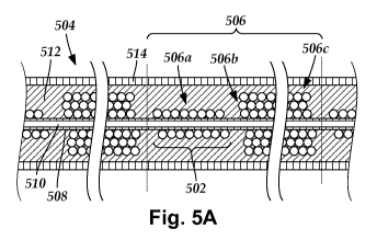
the inner insulation layer. Figure 5A is a schematic longitudinal cross-
sectional
view of one embodiment of portions of a plurality of conductors 502 disposed
in an
elongated member 504. The illustrated portions of the conductors 502 includes
unit
506, shown between two vertical dotted lines. Unit 506 includes a first
conductor
segment 506a, a second conductor segment 506b, and a third conductor segment
506c. In at least some embodiments, the conductors 502 are disposed over a
conductor placement sleeve 508. In at least some embodiments, the conductor
placement sleeve 508 defines a lumen 510.
An inner insulation layer 512 is disposed over the conductors 502. An outer
insulation layer 514 is disposed over the inner insulation layer 512. In at
least some
embodiments, the outer insulation layer 514 is disposed over the inner
insulation
layer 512 such that the elongated member 504 has a uniform transverse diameter
along a longitudinal length of the elongated member 504. In Figure 5A, the
conductors 502 are completely encased in the inner insulation layer 512.
Figure 5B
is a schematic longitudinal cross-sectional view of another embodiment of
portions
of the plurality of conductors 502 disposed in the elongated member 504. In
Figure
513, the conductors 502 are partially encased in the inner insulation layer
512 and
partially encased in the outer insulation layer 514.
In at least some embodiments, the inner insulation layer 512 penetrates and
fills empty spaces along a longitudinal length of the elongated member 502 not
occupied by the conductors including, for example, spaces between adjacent
units,
spaces between individual coils of one of the conductor segments, spaces
between
two or more of the conductors 502.
In at least some embodiments, the inner insulation layer 512 is a flowable
material that penetrates and fills in open spaces formed around the conductors
502
disposed in the elongated member 504. In at least some embodiments, the outer
insulation layer 514 is a more durable than the inner insulation layer 512. In
at least
WO 2010/117678 PCT/US2010/028819
14
some embodiments, the outer insulation layer 514 is more rigid than the inner
insulation layer 512. In at least some embodiments, the outer insulation layer
514 is
substantially more rigid than the inner insulation layer 512. In at least some
embodiments, the outer insulation layer 514 forms a shell around the inner
insulation
layer 512.
The inner insulator layer 512 can be formed from any suitable non-
conductible, biocompatible material adapted to flow when applied to the
elongated
member 504 including, for example, silicone elastomers, hydrogels,
polyurethane,
other thermoplastic polymers, and the like or combinations thereof. In at
least some
embodiments, the inner insulator layer 512 is formed from a material that may
set or
cross-link after flowing, for example, as temperature is lowered or when
irradiated
with light (e.g., visible, ultraviolet, or infrared) or when heated to a cross-
linking
activation temperature. In at least some embodiments, the inner insulator
layer 512
is formed from a doped material, or a composite material (e.g., a material
filled with
glass, carbon fiber, or the like). In at least some embodiments, the inner
insulator
layer 512 is a foam. In at least some embodiments, the inner insulator layer
512 is
configured and arranged to couple (e.g., adhere, or the like) with one or more
of the
conductor placement sleeve 508, electrodes (see e.g., 134 of Figure 1),
terminals
(see e.g., 310 of Figure 3A), or conductive contacts (see e.g., 340 of Figure
3B). In
at least some embodiments, the material used to form the inner insulator layer
512
varies along the length of the elongated member 504.
The inner insulator layer 512 may be disposed over and between the
conductors 502 using many different techniques or processes including, for
example,
dip coating, injection molding, or other coating or molding techniques. Other
coating and molding techniques may include extrusion, passing an outer sleeve
of
material (e.g., an outer insulator layer) around the conductors and injecting
the inner
insulator layer into the sleeve, pre-filling a sleeve with the inner insulator
layer and
then pulling the filled sleeve over the conductors, or the like or
combinations
thereof. In at least some embodiments, some of the abovelisted techniques or
processes may be performed while placing the conductor in a vacuum to evacuate
air
pockets or draw material into open spaces.
WO 2010/117678 PCT/US2010/028819
An outer insulator layer 514 is disposed over at least a portion of the inner
insulator layer 512. The outer insulator layer 514 can be formed from any
suitable
non-conductible, biocompatible material adapted to be non-flowing at
temperatures
at or below body temperature including, for example, silicone elastomers,
hydrogels,
5 other thermoplastic polymers, other thermoset materials, and the like or
combinations thereof. Employing an outer insulator layer formed from a
thermoplastic may have an advantage of being potentially weldable, either
directly
or indirectly, to electrodes (see e.g., 134 in Figures 1) or terminals (see
e.g., 310 of
Figure 3A). In at least some embodiments, the outer insulator layer 514 is
formed
10 from a doped material, or a composite material (e.g., a material filled
with glass,
carbon fiber, or the like). In at least some embodiments, the outer insulator
layer
514 is configured and arranged to bond with one or more of electrodes (see
e.g., 134
of Figure 1), terminals (see e.g., 310 of Figure 3A), or conductive contacts
(see e.g.,
340 of Figure 3B). In at least some embodiments, the material used to form the
15 outer insulator layer 514 varies along the length of the elongated member
504.
The outer insulator layer 514 may be disposed over the conductors 502 using
many different techniques or processes including, for example, dip coating,
injection
molding, or other coating or molding techniques. Other techniques may include
extrusion, reflowing the outer insulator layer using thermal methods (e.g., a
sleeve
fitted over and then reflowed by heating), and the like or combinations
thereof. In at
least some embodiments, some of the abovelisted techniques or processes may be
performed while placing the conductors 502 in a vacuum to evacuate air
pockets.
In at least some embodiments, the outer insulator layer 514 forms a smooth
outer surface along at least a portion of the longitudinal length of the
elongated
member 504. In at least some embodiments, one or more additional layers of
material may be utilized in addition to the inner insulator layer 512 and the
outer
insulator layer 514 including, for example, one or more layers of material
between
the conductor and the inner insulator layer 512, one or more layers of
material
between the inner insulator layer 512 and the outer insulator layer 514, or
one or
more layers of material disposed over the outer insulator layer 514.
It will be understood that an insulator layer may include one or more
applications of the same material to the conductors 502 over a period of time.
It will
WO 2010/117678 PCT/US2010/028819
16
also be understood that an insulator layer may include one or more combined
parts
that collectively form the insulator layer (e.g., two or more combined
materials). It
will additionally be understood that an insulator layer may, by itself, or by
the
inclusion one or more additives combined with the one or more materials,
effect one
or more mechanical properties, or characteristics, of the insulator layers
including,
for example, rigidity, flexibility, melting point, viscosity, and the like or
combinations thereof. In at least some embodiments, the inner insulator layer
512
may serve as a heat shield to protect one or more conductors 502 during
subsequent
processing steps including, for example, thermoforming the outer insulator
layer 514
around the inner insulator layer 512.
In at least some embodiments, the inner insulator layer 512 is more flexible
than the outer insulator layer 514. In at least some embodiments, the outer
insulator
layer 514 is more flexible than the inner insulator layer 512. In at least
some
embodiments, the flexibility of the elongated member 504 may be adjusted by
varying the flexibility of either, or both, the inner insulator layer 512 or
the outer
insulator layer 514. In at least some embodiments, the combination of
materials
used to form the inner insulator layer 512 and the outer insulator layer 514
improve
the flex fatigue properties of the elongated member 504. In other words, in at
least
some embodiments, the combination of materials used to form the inner
insulator
layer 512 and the outer insulator layer 514 may collectively reduce the forces
transmitted to the conductors 502, as compared to conventional jacketing
material.
It will be understood that an insulator layer may, by itself, or by the
inclusion
one or more additives combined with the one or more materials, effect one or
more
electromagnetic properties, or characteristics, of the insulator layers
including, for
example, conductance, inductance, capacitance, or the like. In at least some
embodiments, one or more of the conductance, inductance, or capacitance
properties
are only altered when exposed to certain frequency ranges. For example, in at
least
some embodiments, one or more of the conductance, inductance, or capacitance
properties are only altered when exposed to frequency ranges at or around
frequencies used during MRI procedures (e.g., 64 MHz, 128 MHz, or the like).
In at least some embodiments, the inner insulator layer 512 may be modified,
or may include one or more materials, for eliminating or reducing the effect
of RF
WO 2010/117678 PCT/US2010/028819
17
radiation on the one or more conductors 502. For example, the inner insulator
layer
512 may be modified, or may include one or more materials, for altering one or
more of the dielectric properties (e.g., capacitance or the inductance) of the
one or
more conductors 502. In at least some embodiments, at least one of the
insulator
layers can be made lossy, such as by inclusion of conductive elements, thereby
lowering resonant behavior of currents flowing in one or more encased
conductors
502.
Figure 6 is a schematic overview of one embodiment of components of an
electrical stimulation system 600 including an electronic subassembly 610
disposed
within a control module. It will be understood that the electrical stimulation
system
can include more, fewer, or different components and can have a variety of
different
configurations including those configurations disclosed in the stimulator
references
cited herein.
Some of the components (for example, power source 612, antenna 618,
receiver 602, and processor 604) of the electrical stimulation system can be
positioned on one or more circuit boards or similar carriers within a sealed
housing
of an implantable pulse generator, if desired. Any power source 612 can be
used
including, for example, a battery such as a primary battery or a rechargeable
battery.
Examples of other power sources include super capacitors, nuclear or atomic
batteries, mechanical resonators, infrared collectors, thermally-powered
energy
sources, flexural powered energy sources, bioenergy power sources, fuel cells,
bioelectric cells, osmotic pressure pumps, and the like including the power
sources
described in U.S. Patent Application Publication No. 2004/0059392,
incorporated
herein by reference.
As another alternative, power can be supplied by an external power source
through inductive coupling via the optional antenna 618 or a secondary
antenna.
The external power source can be in a device that is mounted on the skin of
the user
or in a unit that is provided near the user on a permanent or periodic basis.
If the power source 612 is a rechargeable battery, the battery may be
recharged using the optional antenna 618, if desired. Power can be provided to
the
battery for recharging by inductively coupling the battery through the antenna
to a
WO 2010/117678 PCT/US2010/028819
18
recharging unit 616 external to the user. Examples of such arrangements can be
found in the references identified above.
In one embodiment, electrical current is emitted by the electrodes 134 on the
paddle or lead body to stimulate nerve fibers, muscle fibers, or other body
tissues
near the electrical stimulation system. A processor 604 is generally included
to
control the timing and electrical characteristics of the electrical
stimulation system.
For example, the processor 604 can, if desired, control one or more of the
timing,
frequency, strength, duration, and waveform of the pulses. In addition, the
processor
604 can select which electrodes can be used to provide stimulation, if
desired. In
some embodiments, the processor 604 may select which electrode(s) are cathodes
and which electrode(s) are anodes. In some embodiments, the processor 604 may
be
used to identify which electrodes provide the most useful stimulation of the
desired
tissue.
Any processor can be used and can be as simple as an electronic device that,
for example, produces pulses at a regular interval or the processor can be
capable of
receiving and interpreting instructions from an external programming unit 608
that,
for example, allows modification of pulse characteristics. In the illustrated
embodiment, the processor 604 is coupled to a receiver 602 which, in turn, is
coupled to the optional antenna 618. This allows the processor 604 to receive
instructions from an external source to, for example, direct the pulse
characteristics
and the selection of electrodes, if desired.
In one embodiment, the antenna 618 is capable of receiving signals (e.g., RF
signals) from an external telemetry unit 606 which is programmed by a
programming unit 608. The programming unit 608 can be external to, or part of,
the
telemetry unit 606. The telemetry unit 606 can be a device that is worn on the
skin
of the user or can be carried by the user and can have a form similar to a
pager,
cellular phone, or remote control, if desired. As another alternative, the
telemetry
unit 606 may not be worn or carried by the user but may only be available at a
home
station or at a clinician's office. The programming unit 608 can be any unit
that can
provide information to the telemetry unit 606 for transmission to the
electrical
stimulation system 600. The programming unit 608 can be part of the telemetry
unit
606 or can provide signals or information to the telemetry unit 606 via a
wireless or
WO 2010/117678 PCT/US2010/028819
19
wired connection. One example of a suitable programming unit is a computer
operated by the user or clinician to send signals to the telemetry unit 606.
The signals sent to the processor 604 via the antenna 618 and receiver 602
can be used to modify or otherwise direct the operation of the electrical
stimulation
system. For example, the signals may be used to modify the pulses of the
electrical
stimulation system such as modifying one or more of pulse duration, pulse
frequency, pulse waveform, and pulse strength. The signals may also direct the
electrical stimulation system 600 to cease operation, to start operation, to
start
charging the battery, or to stop charging the battery. In other embodiments,
the
stimulation system does not include an antenna 618 or receiver 602 and the
processor 604 operates as programmed.
Optionally, the electrical stimulation system 600 may include a transmitter
(not shown) coupled to the processor 604 and the antenna 618 for transmitting
signals back to the telemetry unit 606 or another unit capable of receiving
the
signals. For example, the electrical stimulation system 600 may transmit
signals
indicating whether the electrical stimulation system 600 is operating properly
or not
or indicating when the battery needs to be charged or the level of charge
remaining
in the battery. The processor 604 may also be capable of transmitting
information
about the pulse characteristics so that a user or clinician can determine or
verify the
characteristics.
The above specification, examples and data provide a description of the
manufacture and use of the composition of the invention. Since many
embodiments
of the invention can be made without departing from the spirit and scope of
the
invention, the invention also resides in the claims hereinafter appended.