Note: Descriptions are shown in the official language in which they were submitted.
CA 02757946 2011-10-06
TAP CHANGER WITH SEMICONDUCTOR SWITCHING ELEMENTS
The invention relates to a tap changer with semiconductor
switching elements for uninterrupted switching over between winding
taps of a tapped transformer.
Such a tap changer is known from WO 97/05536
[US 5,969,511). In this known tap changer two load branches
connectable with the respective winding taps are provided, wherein
each of the two load branches is connectable by the semiconductor
switching elements and can be electrically connected with a common
load shunt. By contrast to usual tap changers with mechanical
contacts for load switching over or also the tap changer with
vacuum switching cells for load switching over, the known tap
changer with semiconductor switching elements does not require any
switch-over resistances
It is disadvantageous with this known tap changer that
electronic power semiconductor switching elements are constantly
loaded, even in unchanging operation, by the respective tap
voltage.
It is the object of the invention to eliminate this
disadvantage in the case of a tap changer according to category and
to indicate a solution in which the electronic power components are
cleared in unchanging operation.
A tap changer with a thyristor pair is, in fact, already
known from WO 88/10502 [US 5,006,784]. in which in unchanging
operation the current feed is taken over by a mechanical permanent
main contact However, this solution concerns a so-termed hybrid
switch with a separate load changeover switch with numerous
- 1 -
CA 02757946 2011-10-06
mechanical contacts, in which with use of a force store a rapid
switching over between the two winding taps of the tapped
transformer is realized by means of a switch-over resistance which
can be temporarily switched on. In the case of the invention,
thereagainst, there shall be no need at all for switch-over
resistances.
The set object is fulfilled by a tap changer with the
features of the first patent claim. The subclaims relate to
particularly advantageous developments of the invention.
In this regard, the general inventive concept is based on
providing a movable contact carriage of electrically insulating
material on which several electrically conductive contact bridges
are fixedly arranged and can be moved together with the contact
carriage between the winding taps Accordingly, in the case of each
switching over a movement in common of all contact bridges from the
winding tap which is to be left to the winding tap which is to be
switched over to takes place According to the invention, one of the
contact bridges, namely the shunt contact bridge, on each occasion
in the unchanging state directly connects the currently connected
winding tap, i.e. the corresponding fixed contact of the tap
changer, with the load shunt.
Overall, in the case of the invention a simple switching
over as well as a simple contacting or connecting of the
semiconductor components during switching over in fixed time
sequence, i.e. switching sequence, results due to the respective
contact bridges. Moreover, a switching free, i.e. electrical
unloading of the semiconductor components, takes place in
unchanging operation in simple manner by a further contact bridge,
- 2 -
CA 02757946 2011-10-06
namely the shunt contact bridge, which directly cooperates with the
load shunt.
The invention will be explained in more detail in the
following by way of exemplifying embodiments, in which
FIG. 1 shows a tap changer according to the invention in
schematic illustration and
FIG. 2 shows a further form of embodiment of a tap
changer according to the invention.
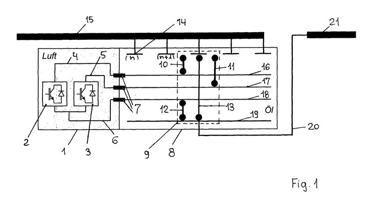
A tap changer comprising an electronic power load
changeover switch 1 is shown in FIG. 1. In that case, two
semiconductor switches 2 and 3 are provided, which each have a
respective electrical input 4 or 5 and have a common electrical
output 6. The electrical inputs 4, 5 and the electrical output 6
are guided by means of passages 7 in a mechanical contact system 8
The mechanical contact system 8 comprises a contact
carriage 9 which is indicated in the figure merely by a dashed
line. The contact carriage 9 has contact bridges 10, 11, 12, 13
fixedly arranged thereon. The contact bridges 10 to 13 are
electrically conductive, but insulated relative to one another;
they have at their ends intrinsically known contact rollers, wiper
arrangements or comparable means, which are merely indicated in the
figure. Each of the tap contacts 14 illustrated in the figure
corresponds with a winding tap n, n + 1, of the regulating winding
15 of the tapped transformer. In addition provided in the
mechanical contact system are three contact rails 16, 17, 18 which
are each electrically conductive and each of which is electrically
connected with a respective one of the electrical input 4, the
- 3 -
CA 02757946 2011-10-06
electrical input 5 and the electrical output 6 of the semiconductor
switches 2, 3.
In addition, a shunt contact rail 19 is arranged in the
mechanical contact system and is electrically connected with the
actual load shunt 20, which in turn leads to the main winding 21 of
the tapped transformer.
In the form of embodiment shown here the contact rails 16
to 18 and the shunt contact rail 19 extend parallel to one another;
in this regard the contact carriage 9 executes a linear,
translational movement for the contact-making.
The first contact bridge 10 can be connected at one of
its free ends with the tap changer contacts 14 and at its other
free end it runs on the contact rail 16, which is electrically
connected with the input 8 of the first semiconductor switch 2.
The second contact bridge 11 can be similarly connected at one free
end thereof with the fixed tap changer contacts 14 and at its other
free end it runs on the further contact rail 17, which is
electrically connected with the input 5 of the second semiconductor
switch 3. The third contact bridge 12 runs by one of its free ends
on the contact rail 18, which is electrically connected with the
common electrical output 6 of the electronic power switch. Its
other free end runs on the shunt contact rail 19. Physically
arranged between the two mentioned contact bridges 10 and 11 is the
further contact bridge 13, namely the shunt contact bridge, which
can be contacted at one free end thereof with the fixed tap changer
contacts 14 and runs at its other end on the shunt contact rail 19.
It can be seen that not only the contact bridge 12 and
thus the common output 6 of the electronic power load changeover
- 4 -
CA 02757946 2011-10-06
switch, but also the contact bridge 13 are electrically connected
with the shunt contact rail 19, i.e. the load shunt 20. In
unchanging operation the contact bridge 13 takes over the direct
electrical connection between the respectively connected tap
changer contact 14 and the load shunt 20. The contact bridges 10
and 11, which lead to the inputs of the electronic power load
changeover switch 1, are, thereagainst, not connected; the
semiconductor switches 2 and 3 are cleared. In the case of a load
changeover the contact carriage 9 is moved to the left or the
right, depending on whether switching is to be in the direction
"higher" or "lower." As a consequence, one of the two contact
bridges 10 and 11 runs onto the new tap changer contact 14 to be
connected and thus produces an electrical connection with the
corresponding input 4 or 5 of the respective semiconductor switch 2
or 3. At the same time the contact bridge 13 comes out of contact.
The switching over is concluded when the contact carriage 9 has
been moved on to such an extent that the contact bridges 10 and 11
both again come out of engagement and the contact bridge 13 has
taken over the permanent current conductance FIG. 2 shows a further
form of embodiment of the invention with a circular arrangement.
Here, too, semiconductor switches 2 and 3 are provided, which each
have a separate electrical input 4 or 5 and which have a common
electrical output 6. Here, contact rollers 22, 23, 24 each running
on a respective contact ring 25, 26, 27 are provided. These
contact rings 25 to 27 correspond in respect to their function with
the contact rails 16 to 18 of FIG. 1. Fixed tap changer contacts
14 are here provided on a concentric circle. Moreover, a shunt
-
- CA 02757946 2011-10-06
ring 28 is shown, which in turn is electrically connected with the
load shunt.
Contact rollers 30, 31, 32, which are contactable with
the fixed tap changer contacts, are provided in a first horizontal
plane on a switch segment 28, which is again indicated only by a
dashed line, of insulating material. Further contact rollers 33,
34, which run on the shunt ring, are provided in a second
horizontal plane.
The contact roller is connected by way of the contact
ring 25 with the input 4 of the first semiconductor switch 2 The
contact roller 32 is connected by way of the contact ring 26 with
the input 5 of the second semiconductor switch 3. The lower
contact roller 33 is connected by way of the contact ring 27 with
the common output 6 of the two semiconductor switches 2 and 3. The
upper contact roller 31 and lower contact roller 34 finally have an
electrically conductive connection 35 in such a manner that the
contact roller 31, which is arranged physically between the contact
rollers 30 and 32, is disposed in direct connection with the load
shunt 28 by way of the lower contact roller 34.
In this form of embodiment the switching segment 29 and
with it the contact rollers 30 to 34 execute a rotational movement
on each occasion of switching over.
However, the principle in terms of function is the same:
in unchanging operation the respectively connected fixed tap
changer contact 48 is directly electrically connected with the
shunt ring 28, whilst the semiconductor switches 2 and 3 are
switched free. Only in the case of switching over is a respective
one of the two inputs 4 and 5 - depending on the rotational
6 -
CA 02757946 2011-10-06
direction - of the electronic power load changeover switch briefly
connected by means of the associated contact roller 30 or 32 with
the respective fixed tap changer contact 14 to be switched over to.
7 -