Note: Descriptions are shown in the official language in which they were submitted.
:A 02758032 2011 08 19
COIN HAVING INTEGRATED RFID IDENTIFICATION DEVICE AND METHOD FOR
THE PRODUCTION THEREOF
The invention relates to a coin and a method for the manufacture of such a
coin.
In the currencies of various countries, coins are used as means of payment and
usually feature an embossment. Such coins are manufactured from at least one
disk-shaped blank or base element of metal or a metal alloy.
Coins are also known that consist of at least two parts, namely one ring-
shaped base
element and one preferably disk-shaped central or core element. The
aforementioned
coin elements can be manufactured for example from different metal materials
to
achieve a special visual appearance of the coins. Single specimens of such
coins
meanwhile have a monetary value that far exceeds the material value of the
respective coin, so that measures are necessary for identifying such coins or
for
verifying that they are genuine.
Also known are contactless identification systems for the identification and
tracing of
movable objects, the systems being permanently connected with the object to be
identified. RFID identification systems are frequently used for this purpose,
which
essentially make use of RFID technology for the transfer of data. The acronym
RFID
stands for "Radio Frequency Identification".
Classic RFID systems consist of a stationary or mobile RFID scanner and an
RFID
transponder, which comprises an RFID chip that interacts with an antenna
assembly.
The RFID scanner also comprises an antenna assembly, by means of which an
electromagnetic field is generated. If the antenna assembly of the RFID
transponder
enters the electromagnetic field of the RFID scanner, an inductive signal
coupling
between the RFID scanner and the RFID transponder occurs. Attenuation
modulation
of the electromagnetic field produced by the RFID scanner achieves at least a
- 1 -
:A 02758032 2011-08-19
directional data transfer, especially of identification information from the
RFID
transponder to the RFID scanner. Such RFID systems operate for example at a
frequency of 125 kHz to 13.56 MHz.
It is also possible to attach extremely flat, preferably passive RFID
transponders,
so-called "smart labels", to the surfaces of objects made of plastic. It
becomes
problematic, however, when such passive RFID transponders are operated in the
immediate proximity of electrically and/or magnetically conductive materials,
especially conductive surfaces with at least a significant metal content,
since the
magnetic alternating flow in the electrically and/or magnetically conductive
material
induces eddy currents, which cause the electromagnetic field generated by the
RFID
scanner on the surface of the respective object to be attenuated so strongly
that the
data transfer of the RFID transponder provided on the surface of the object is
hindered so strongly that the reception of usable data by the RFID scanner is
no
longer possible.
The shielding of such eddy currents poses a technical problem, which in the
case of
RFID technology is caused by the geometry of the antenna structure provided in
the
immediate proximity of the conductive layer. This problem can be solved by
providing
and suitably orienting a shielding layer consisting of highly permeable
materials such
as ferrites or special alloys between the antenna structure formed by at least
one
conductive loop and the metal surface of the object, to cancel the induced
eddy
currents to a large extent. Ferrite foils, for example, are already being used
for
shielding.
Based on the prior art, the object of the invention is to improve a coin to
the extent
that a simple and fast verification of the genuineness of the coin is
possible, to
reliably identify counterfeit coins and worthless copies.
- 2 -
:A 02758032 2011-08-19
The essential aspect of the coin according to the invention is that the flat
insert
element received in the base element of the coin is manufactured from a
non-conductive material, preferably plastic, and that at least one RFID
identification
device is provided in the flat insert element. In an advantageous embodiment,
the
RFID identification device consists of an RFID transponder.
In a further advantageous embodiment the at least one disk-shaped metal base
element comprises at least one recess or hole for receiving the preferably
disk-shaped flat insert element, the insert element forming a plastic casing
for the
RFID identification device. This effectively protects the RFID identification
device or
the RFID transponder during the identification process and during later use of
the
coin with the integrated RFID identification device.
The RFID transponder comprises at least one RFID chip and at least one antenna
structure connected with said chip, the RFID transponder preferably being
designed
as a passive unit without its own energy supply. The RFID chip and the
corresponding
antenna structure can be advantageously applied to a base layer, for example a
thin
paper layer or plastic film and the RFID transponder can comprise at least one
electrically conductive shielding layer for shielding the RFID chip and its
antenna
structure against eddy currents caused by the metal base element.
Further, the invention refers to a method for manufacturing a coin with an
integrated
RFID identification device from a preferably disk-shaped metal base element,
in which
especially advantageously a recess or hole is made in the base element and a
flat
insert element with an RFID identification device received in said insert
element is
inserted into the recess or hole and the flat insert element is pressed
together with
the base element.
The invention is described below based on exemplary embodiments with reference
to
the drawings, in which:
- 3 -
:A 02758032 2011-08-19
Fig. 1 a shows a top view of a conventional coin;
Fig. 1 b shows a cross section through the coin in Figure 1;
Fig. 2 a shows a top view of a disk-shaped base element with a recess or
hole;
Fig. 2 b shows a top view of a flat insert element;
Fig. 2 c shows a cross section through the disk-shaped base element with
the
flat insert element inserted into the hole;
Fig. 2 d shows a cross section through the disk-shaped based element with
the
flat insert element inserted into the recess;
Fig. 3 shows a top view of a flat insert element with integrated RFID
identification device;
Fig. 4 shows a cross section through a disk-shaped base element and
corresponding flat insert element with concave and convex edge
sections and
Fig. 5 shows a cross section through a disk-shaped base element and
corresponding flat insert element with tongue and groove sections.
Figure 1 (a) shows a top view of a coin 1 and Figure 1 (b) shows a cross
section
through the coin 1 according to Figure 1 (a), the coin being designed for use
as a
means of payment. Such coins 1 are sufficiently known in the prior art and are
manufactured in a wide range of forms and shapes.
Such coins 1 used as means of payment normally consist of one or several parts
and
are made of an extremely stable material, namely of metal and/or of a metal
alloy.
They consist essentially of a disk-shaped base element 2 or in the case of
multi-part
coins 1 of a base element 2 and at least one further element received by said
base
element. A coin 1 normally comprises at least one front side 1.1, one reverse
side 1.2
and one edge 1.3.
- 4 -
:A 02758032 2011-08-19
. .
The coin 1 depicted in Figure 1 (a) and (b) furthermore comprises an
embossment 3
on the front and/or reverse side 1.1, 1.2 of the coin 1, by means of which for
example
a numeral indicating the value of the coin 1, a symbol, a picture or various
decorative
elements are applied to the front and/or reverse side 1.1, 1.2 of the coin 1.
The
principle of embossing coins is sufficiently known. In this process, a
preferably metal
coin blank in the form of a disk-shaped base element 2 is placed between an
upper
and a lower die, which respectively bear the negative of the motif to be
embossed.
The upper and lower die are pressed together so that the respective motif is
embossed into the front and reverse side of the base element 2 of the coin 1.
This
reduces in particular also the thickness of the disk-shaped base element 2,
and
through the embossing process an outer ring 2.1 can be formed on the edge of
the
coin 1, which (ring) sticks out upward and downward from the front and/or
reverse
side of the coin 1 formed by the embossing and therefore forms the ring-shaped
bearing surface of the coin 1.
The base element 2 of the coin 1 is preferably disk-shaped and flat in design.
The at
least one further element provided in the case of bimetal coins 1 can likewise
be
manufactured from metal or a metal alloy and is inserted into a recess or hole
2.2
provided in the base element 2, namely preferably in the center area of the
coin 1.
The base element 2 and the further element are bonded with each other or
pressed
together by plastic deformation under pressure. For example, the further
element is
pressed into the recess or hole 2.2 of the base element 2, preferably during a
punch
press process.
For the manufacture of a coin 1 according to the invention with an integrated
RFID
identification device 5, first a metal blank forming the disk-shaped base
element 2 is
provided, which may be designed as having several parts. The disk-shaped base
element 2 already corresponds essentially to the basic form of the coin 1 to
be
- 5 -
:A 02758032 2011-08-19
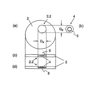
manufactured. Figure 2 (a) shows a top view of the disk-shaped base element 2
for
manufacturing a coin 1.
According to the invention, at least one recess or hole 2.2 is then made in
the
disk-shaped base element 2 and is provided for receiving a flat insert element
4. The
form and cross section of the flat insert element 4 are adapted to the form of
the
recess or the dimensions of the hole 2.2 in the disk-shaped base element 2.
Further, the recess or hole 2.2 can be provided at virtually any position of
the
disk-shaped base element 2, namely both off-center or in the center area of
the coin
1. In a preferred embodiment the flat insert element 4 has a circular cross
section, and
the thickness of the flat insert element 4 is smaller than the chosen
thickness of the
disk-shaped base element 2.
According to the invention the flat insert element 4 is furthermore
manufactured from
a non-conductive material, preferably plastic and at least one RFID
identification
device 5 is provided in the flat insert element 4. Figure 2 (b) shows a top
view of the
insert element 4 according to the invention with integrated RFID
identification device
and Figure 2 (c) and (d) respectively show a cross section through the disk-
shaped
base element 2 with an insert element 4 with integrated RFID identification
device 5
inserted into the hole or recess 2.2. The surface proportion of the flat
insert element 4
in comparison with the surface of the base element 2 of the coin 1 is less
than 5%, so
that the metal character of the coin 1 is retained also after insertion of the
flat insert
element 4 into the base element 2.
The RFID identification device 5 is designed for example as an RFID
transponder,
which consists of an RFID chip 5.1 and an antenna structure 5.2 connected with
said
chip. Figure 3 shows a possible embodiment of such an RFID transponder 5. The
RFID
transponder 5 does not have its own power supply, i.e. it is designed as a
passive unit
and is therefore active only within the response range of an RFID scanner. The
- 6 -
CA 02758032 2015-11-20
electrical power needed for operation of the RFID transponder 5 or of the RFID
chip 5.1 is
received in the known manner from the RFID scanner (not depicted in the
drawings) via the
antenna structure 5.2 and transmitted to the RFID chip 5.1.
To reduce the installed depth of the RFID transponder 5, it can be designed
for
example in the form of a transponder inlay, i.e. the RFID chip 5.1 and the
corresponding
antenna structure 5.2 are applied to a base layer 5.3, for example a thin
paper layer or plastic
film. The antenna structure 5.2 is normally laminated onto the base layer 5.3
as a full-
surface copper or aluminum foil, coated with light-sensitive photoresist and
after exposure
the areas corresponding to the antenna structure 5.2 are etched free in a
caustic bath.
Afterwards, the RFID chip 5.1 is placed on the connecting areas of the
resulting antenna
structure 5.2 and bonded conductively with these areas. The antenna structure
5.2 of the
RFID transponder 2 forms for example a dipole or an induction loop. This
results in an
RFID transponder 5 with an extremely flat design.
In a preferred embodiment in the case of insertion of the insert element 4 in
a recess 2.2
of the disk-shaped base element 2 according to Figure 2(d), and electrically
conductive
shielding layer, in particular a metal foil is provided on the side of the
base layer 5.3 opposing
the antenna structure 5.2, which (shielding layer) approximately corresponds
to the spatial
dimensions of the antenna structure 5.2. Such an electrically conductive
protective layer
enables effective shielding of the RFID chip 5.1 or its antenna structure 5.2
from eddy currents
caused by the metal base element 2 is possible. The ferromagnetic particles of
the electrically
conductive shielding layer are oriented so that after being fixed on the base
layer 5.3 they are
parallel to a magnetic field induced in the antenna structure 5.2 of the RFID
transponder 5 and
therefore effectively suppress eddy currents which occur.
- 7 -
:A 02758032 2011-08-19
For manufacturing the flat insert elements 4 the RFID transponder 5 is
surrounded by
a plastic casing 6 or plastic is molded around the RFID transponder 5,
providing
effective protection of the RFID transponder 5 from external influences. An
injection
molding process can be used for this, for example. The plastic used for this
preferably
has the same color as the base element 2.
The plastic casing 6 can also contain ceramic and/or metal particles. The RFID
transponder 5 integrated in the plastic casing 6 or the flat, preferably disk-
shaped
insert element 4 thus formed is inserted as described below into the recess or
hole 2.2
of the base element 2.
In a first embodiment variant the diameter DE of the circular insert element 4
approximately corresponds to the diameter DB of the recess or hole 2.2, i.e.
there is
practically no play between the diameter DE of the insert element 3 and the
diameter
DB of the recess or hole 2.2. For insertion of the flat, disk-shaped insert
element 4 into
the recess or hole 2.2 the insert element 4 is positioned over the recess or
hole 2.2
and pressed by means of a pressing process into the recess or hole 2.2. This
results in
a pressed connection between the base element 2 and the insert element 4. This
is
followed by embossment of the coin and application of any further protective
layers,
such as a lacquer or color coating.
According to a second embodiment variant the diameter DE of the circular
insert
element 4 is smaller than the diameter DB of the recess or hole 2.2, i.e. the
play
between the diameter DE of the insert element 4 and the diameter DB of the
recess or
hole 2.2 is sufficient to insert the insert element 4 without considerable
force into the
recess or hole 2.2 of the base element 2. For fixing the insert element 4 in
the recess
or hole 2.2 of the base element 2, at least the base element 2 is deformed by
means
of a subsequent pressing process so that the diameter DB of the recess or hole
2.2
decreases, causing the insert element 4 to be fixed in the base element 2.
This is
- 8 -
:A 02758032 2011 08 19
followed by embossing of the base element 2 to form the coin 1, as described
for the
previous embodiment variant.
The base element 2 of the coin 1 prior to the pressing and/or embossing
process has
a thickness for example of 2.0 to 3.0 mm, preferably 2.25 mm. After the
pressing
and/or embossing process the thickness is between 1.5 and 2.0 mm, preferably
1.8 mm. The thickness of the flat insert element 4 is significantly less than
the
thickness of the base element prior to the pressing and/or embossing process,
namely between 1.5 and 2.0 mm, preferably approximately 1.8 mm.
Preferably the press die provided for the pressing process is designed so that
it has a
convex bulge in the direction of the base element 2, so that an outward
pressing
force is exerted on the base element 2 during the pressing process. During the
pressing process at least the base element 2 is impinged with a pressing force
between 100 and 250 Nm.
To prevent damage to the RFID identification device 5 integrated in the insert
element 4 through the embossing process, the press die can have a recess in
the area
of the RFID identification device 5, the recess corresponding in form and
dimensions
to those of the insert element 4. Also, for forming the outer edge 2.1 of the
coin 1,
the chosen diameter of the press die can be smaller than the diameter of the
base
element 2.
To increase the bond strength, in a preferred embodiment the outer edge 4' of
the
insert element 3' and the inner edge 2.2' of the recess or hole 2.2 are
designed for
creating a form-fitting connection. In particular, according to the exemplary
embodiment depicted in Figure 4, the outer edge 4' of the insert element 3'
can be
concave and the inner edge 2.2' of the recess or hole 2.2. can be convex, or
vice versa.
- 9 -
:A 02758032 2011 08 19
Likewise, according to the exemplary embodiment depicted in Figure 5, the
form-fitting connection can be achieved as a tongue-and-groove connection,
namely
for example with the outer edge 4 of the insert element 3' having at least one
tongue
and the inner edge 2.2' of the recess or hole 2.2 having at least one groove,
or vice
versa.
The invention was described above based on an exemplary embodiment. It goes
without saying that numerous modifications and variations of the invention are
possible without abandoning the underlying inventive idea.
- 10-
:A 02758032 2011 08 19
Reference list
1 coin
1.1 front
1.2 reverse
1.3 edge of coin
2 base element
2.1 outer ring
2.2 recess or hole
2.2' inner edge
3 embossment
4 insert element
4' outer edge
RFID identification device or RFID transponder
5.1 RFID chip
5.2 antenna structure
5.3 base layer
6 plastic casing
DE diameter of circular insert element
DB diameter of recess or hole
-11 -