Note: Descriptions are shown in the official language in which they were submitted.
CA 02758157 2011-10-06
DESCRIPTION
BONDING UNIT CONTROL UNIT
AND MULTI-LAYER BONDING METHOD
Technical Field
The present invention is related to a bonding
unit control unit and a multi-layer bonding method,
and especially, to a bonding unit control unit and a
multi-layer bonding method, which are used when a
plurality of substrates are bonded to one substrate.
Background Technique
A MEMS device is known in which miniature
electronic parts and machine parts are integrated. As
the MEMS device, a micro-relay, a pressure sensor, an
acceleration sensor, and so on are exemplified. A
room temperature bonding is known in which wafer
surfaces activated in a vacuum atmosphere are
contacted and bonded. Such a room temperature bonding
is suitable for production of the MEMS device. The
MEMS device is demanded to have multi-function so that
one device is provided with a mechanism section and a
circuit section. In such a room temperature bonding,
it is demanded to bond three or more wafers into one
substrate. Moreover, it is necessary to improve mass
productivity in such a room temperature bonding, and
CA 02758157 2011-10-06
- 2 -
it is demanded to bond three or more wafers at higher
speed.
In JP 2008-288384A, a 3-dimensional stacking
device with high reliability is disclosed. In the 3-
dimensional stacking device, each of devices is formed
after the plurality of semiconductor wafers are
stacked and unified. In the two semiconductor wafers
to be stacked, one of the semiconductor wafers has a
convex bonding section and the other of the
semiconductor wafers has a concave section. The
convex section of the semiconductor wafer is directly
bonded with the concave section of the other
semiconductor wafer.
A 3-dimensional LSI stacking device is
disclosed in JP H05-160340A, in which the positions of
an interlayer device could be adjusted precisely and
bonded. In the 3-dimensional LSI stacking device, a
roughly moving stage of a large-stroke low-solution
has 4 or more control axes of X, Y, and Z axes and one
of the rotation axes OX, OY, and ez around the above 3
axes. A finely moving stage of a small-stroke high-
resolution had 6 control axes of X, Y, and Z axes and
the rotation axes OX, OY, and OZ around the above 3
axes. Two wafers can be aligned in the X and Y
directions and positioned in the Z direction by the
roughly moving stage and the finely moving stage. A
sensor senses a distance between the two wafers in the
CA 02758157 2011-10-06
- 3 -
Z direction which is a vertical direction. A load
cell detects a load in the wafer bonding. A position
detecting section detects a position deviation in the
X and Y directions which indicate a plane direction of
each of the wafers. A hardening & bonding section
bonds the two wafers with adhesive by hardening the
adhesive. A movement mechanism positions both of the
position detecting section and the hardening & bonding
section. Thus, the two wafers are positioned in the X
and Y directions by performing a closed loop control
of the roughly moving stage and the finely moving
stage by a control unit based on position deviations
in the X and Y directions of the two wafers detected
by said position detecting section. Also, a
parallelism adjustment of the two wafers and the
pressing of the two wafers are performed by performing
a closed loop control of the roughly moving stage and
the finely moving stage by the control unit based on
the distance detected by said sensor and the load
detected by the load cell.
A method of manufacturing a stacking
structure is disclosed in JP 2004-358602A, in which
the stacking structure of the height of 100 pm or more
is manufacture in a high yield in a short time. In
the method of manufacturing the stacking structure, a
donor substrate is prepared in which a plurality of
section pattern members corresponding to the section
CA 02758157 2011-10-06
52313-16
- 4 -
pattern of the structure are formed. A target substrate is arranged to
oppose to the donor substrate. By repeating a process of positioning
and pressing the target substrate and the section pattern and then
leaving, the section pattern member is transcribed. In such a
manufacturing method of the stacking structure, the preparation of
the donor substrate includes a first process of forming an inversion
pattern layer obtained by inverting the section pattern of the structure
on said donor substrate, a second process of forming the plurality of
section pattern members by plating a spatial portion corresponding to
the section pattern of the structure of the inversion pattern layer, and
a third process of removing said inversion pattern layer.
Citation List:
[Patent Literature 1]: JP 2008-288384A
[Patent Literature 2]: JP H05-160340A
[Patent Literature 3]: JP 2004-358602A
Summary of the Invention
One subject matter of the present invention is to provide a
bonding unit control unit and a multi-layer bonding method, in which,
in some embodiments, three or more substrates are bonded into one
bonded substrate at
CA 02758157 2011-10-06
52313-16
- 5 -
high speed.
Another subject matter of the present invention is to provide a
bonding unit control unit and a multi-layer bonding method, in which,
in some embodiments, three or more substrates are bonded into one
bonded substrate at low cost.
Still another subject matter of the present invention is to
provide a bonding unit control unit and a multi-layer bonding method,
in which, in some embodiments, displacement of three or more
substrates can be prevented.
A multi-layer bonding method of the present invention
includes: forming a first bonded substrate by bonding a first substrate
and an intermediate substrate in a bonding chamber; conveying a
second substrate inside the bonding chamber when the first bonded
substrate is arranged inside the bonding chamber; and forming a
second bonded substrate by bonding the first bonded substrate and
the second substrate in the bonding chamber. According to such a
multi-layer bonding method, after the first substrate is bonded with
the intermediate substrate, the bonded substrate can be bonded by
the second substrate without being taken out from the bonding
chamber. Therefore, the second bonded substrate can be at high
speed at a low cost.
In some embodiments, the intermediate substrate is conveyed
into the bonding chamber in a state that the intermediate substrate is
CA 02758157 2011-10-06
52313-16
- 6 -
put on an intermediate cartridge. The first substrate and the
intermediate substrate are bonded in the state that the intermediate
substrate is put on the intermediate cartridge. The intermediate
cartridge is conveyed from the bonding chamber in the state that the
first bonded substrate is not put on the intermediate cartridge, after
the first substrate and the intermediate substrate are bonded. The
second substrate is conveyed into the bonding chamber in a state
that is put on a cartridge, after the intermediate cartridge is conveyed
out from the bonding chamber. Preferably, the first bonded substrate
and the second substrate are bonded in the state that the second
substrate is put on the cartridge.
In some embodiments, a load applied between the second
substrate and the first bonded substrate when the second substrate
and the first bonded substrate are bonded is preferably larger than a
load applied between the first substrate and the intermediate
substrate when the first substrate and the intermediate substrate are
bonded.
Preferably, the multi-layer bonding method further includes:
activating opposing surfaces of the intermediate substrate and the
first substrate before the first substrate and the intermediate
substrate are bonded; and activating opposing surfaces of the second
substrate and the first bonded substrate before the first bonded
substrate and the second substrate are bonded.
CA 02758157 2011-10-06
52313-16
- 7 -
Preferably, the multi-layer bonding method further includes:
aligning the first substrate and the intermediate substrate before the
first substrate and the intermediate substrate are bonded; and
aligning the first bonded substrate and the second substrate before
the first bonded substrate and the second substrate are bonded.
Preferably, the multi-layer bonding method further includes:
producing the intermediate substrate by processing a third bonded
substrate produced by bonding two substrates.
Preferably, the multi-layer bonding method further includes:
producing a plurality of devices by doing the second bonded
substrate.
In some embodiments, the multi-layer bonding method further
includes: decompressing an internal space of the load lock chamber,
when the cartridge is arranged in the load lock chamber and the
second substrate is put on the cartridge. The second substrate is
conveyed from the load lock chamber into the bonding chamber, after
the internal space of the load lock chamber is decompressed. The
cartridge is provided with island portions contacting the second
substrate when the second substrate is put on the cartridge.
Passages are provided for the island portions to connect a space
CA 02758157 2011-10-06
52313-16
- 8 -
between the cartridge and the second substrate to an outside, when
the second substrate is put on the cartridge. The gas filling the
space is exhausts outside through the passages when the internal
space of the load lock chamber is decompressed. Therefore, in such
a cartridge, it is possible to prevent the second substrate from
moving with respect to the cartridge due to the gas when the
atmosphere is decompressed.
A bonding unit control unit of the present invention includes: a
driving section configured to control a pressure bonding mechanism
to bond a first substrate and an intermediate substrate in a bonding
chamber; and a conveying section configured to control a
conveyance unit to convey a second substrate into the bonding
chamber, when a first bonded substrate formed by bonding the first
substrate and the intermediate substrate is arranged in the bonding
chamber. The driving section controls the pressure bonding
mechanism to bond the first bonded substrate and the second
substrate in the bonding chamber. According to such a bonding unit
control unit, the first substrate can be bonded with the second
substrate without being taken out from the bonding chamber, after the
first substrate is bonded with the intermediate substrate. Therefore,
the second bonded substrate can be at high speed at a low cost.
In some embodiments, the intermediate substrate is conveyed
into the bonding chamber in a state that the intermediate substrate is
put on an intermediate cartridge. The first substrate and the
CA 02758157 2011-10-06
52313-16
- 9 -
intermediate substrate are bonded in the state that the intermediate
substrate is put on the intermediate cartridge. The intermediate
cartridge is conveyed out from inside the bonding chamber in a state
that the first bonded substrate is not put on the intermediate
cartridge, after the first substrate and the intermediate substrate are
bonded. A second substrate is conveyed into the bonding chamber in
a state that the second substrate is put on a cartridge, after the
intermediate cartridge is conveyed out from the bonding chamber.
The first bonded substrate and the second substrate are desirably
bonded in a state that the second substrate is put on the cartridge.
Preferably, the driving section drives the pressure bonding
mechanism such that a load applied between the second substrate
and the first bonded substrate when the second substrate and the
first bonded substrate are bonded is larger than a load applied
between the first substrate and the intermediate substrate when the
first substrate and the intermediate substrate are bonded.
In some embodiments, the bonding unit control unit further
includes: an activating section configured to control an activating unit
such that opposing surfaces of the intermediate substrate and the
first substrate are activated before the first substrate and the
intermediate substrate are bonded. The driving section controls the
activating unit such that opposing surfaces of the second substrate
CA 02758157 2011-10-06
52313-16
- 10 -
and the first bonded substrate are activated before the first bonded
substrate and the second substrate are bonded.
In some embodiments, the bonding unit control unit further
includes: an aligning section configured to control an alignment
mechanism to align the first substrate and the intermediate substrate
before the first substrate and the intermediate substrate are bonded.
The aligning section controls the alignment mechanism to align the
first bonded substrate and the second substrate, before the first
bonded substrate and the second substrate are bonded.
In some embodiments, the conveying section decompresses
an internal space of the load lock chamber, when the cartridge is
arranged in the load lock chamber and the second substrate is put on
the cartridge. The second substrate is conveyed from the load lock
chamber into the bonding chamber, after the internal space of the
load lock chamber is decompressed. Island portions are provided for
the cartridge to contact the second substrate, when the second
substrate is put on the cartridge. Passages are provided for the
island portions to connect a space between the cartridge and the
second substrate to an outside when the second substrate is put on
the cartridge.
In the bonding unit control unit and the multi-layer bonding
method by the present invention, three or more substrates can be
bonded as one bonded substrate at high speed.
CA 02758157 2014-04-09
52313-16
- 10a -
According to one aspect of the present invention,
there is provided a multi-layer bonding method comprising:
forming a first bonded substrate by bonding a first substrate
and an intermediate substrate in a bonding chamber by using a
pressure bonding mechanism; holding said first bonded substrate
by said pressure bonding mechanism in said bonding chamber;
conveying a second substrate into said bonding chamber; and
forming a second bonded substrate by bonding said first bonded
substrate and said second substrate in said bonding chamber by
using said pressure bonding mechanism.
According to another aspect of the present
invention, there is provided a bonding unit control unit
comprising: a first driving section configured to drive a
pressure bonding mechanism to bond a first substrate placed on
a lower carriage and an intermediate substrate held by said
pressure bonding mechanism in a bonding chamber so as to form a
first bonded substrate, to hold said first bonded substrate
after said first bonded substrate is formed, and to bond a
second substrate placed on said lower carriage and said first
bonded substrate held by said pressure bonding mechanism in a
bonding chamber so as to form a second bonded substrate; and a
second driving section configured to drive a conveyance unit to
convey said second substrate onto said lower cartridge in said
bonding chamber, after said first bonded substrate is held by
said pressure bonding mechanism.
CA 02758157 2011-10-06
52313-16
-11 -
Brief Description of the Drawings
FIG. 1 is a sectional view showing a bonding unit;
FIG. 2 is a perspective view showing a stage cartridge;
FIG. 3 is a plan view showing a hand of a conveyance
mechanism;
FIG. 4 is a plan view showing an upper-side cartridge;
FIG. 5 is a sectional view showing wafer positioning pins;
FIG. 6 is a sectional view showing the upper-side cartridge;
FIG. 7 is a sectional view showing a positioning pin;
FIG. 8 is a plan view showing the lower-side cartridge;
FIG. 9 is a sectional view showing the lower-side cartridge;
FIG. 10 is a plan view showing an alignment mechanism;
FIG. 11 is a block diagram showing a bonding unit control unit
according to the present invention;
FIG. 12 is a flow chart showing an operation executed by
using a bonding unit;
CA 02758157 2011-10-06
52313-16
- 12 -
FIG. 13 is a side view showing an example of a state of a
bonding object at step S1;
FIG. 14 is a side view showing an example of the state of the
bonding object at step S3;
FIG. 15 is a side view showing an example of another state of
the bonding object at step S3;
FIG. 16 is a side view showing an example of the state of the
bonding object at step S4;
FIG. 17 is a side view showing an example of the state of the
bonding object at step S12;
FIG. 18 is a side view showing an example of the state of the
bonding object at step S13;
FIG. 19 is a side view showing an example of another state of
the bonding object at step S13;
FIG. 20 is a side view showing example of the state of the
bonding object at step S14;
FIG. 21 is a side view showing an example of another state of
the bonding object at step S14; and
FIG. 22 is a sectional view showing the state that the wafer is
put on a cartridge of the comparison example.
CA 02758157 2011-10-06
52313-16
- 13 -
Description of Embodiments
Hereinafter, a bonding unit control unit according to an
embodiment of the present invention will be described with reference
to the attached drawings. As shown in FIG. 1, the bonding unit
control unit 10 is used for a bonding system. That is, the bonding
system is provided with a bonding unit control unit 10 and a bonding
unit 1. The bonding unit 1 is provided with a bonding chamber 2 and
a load lock chamber 3. The bonding chamber 2 and the load lock
chamber 3 are containers which shield the internal spaces of the
chambers from environment. Moreover, the bonding unit 1 is
provided with a gate valve 5. The gate valve 5 is interposed between
the bonding chamber 2 and the load lock chamber 3. The gate valve
5 is opened or closed to connect the internal space of the bonding
chamber 2 and the internal space of the load lock chamber 3, through
the control by the bonding unit control unit 10. The load lock
chamber 3 is provided with a lid (not shown). The lid closes or opens
a gate which connects the internal space of the load lock chamber 3
with the outside.
The load lock chamber 3 is provided with a vacuum pump 4.
The vacuum pump 4 is controlled by the
CA 02758157 2011-10-06
- 14 -
bonding unit control unit 10 to exhaust gas from the
internal space of the load lock chamber 3. As the
vacuum pump 4, a turbo-molecular pump, a cryopump, and
an oil diffusion pump are exemplified. Moreover, the
load lock chamber 3 is provided with a conveyance
mechanism 6 therein. The conveyance mechanism 6 is
controlled by the bonding unit control unit 10 to
convey a wafer or a substrate arranged in the load
lock chamber 3 through the gate valve 5 to the bonding
chamber 2, or to convey the wafer arranged in the
bonding chamber 2 through the gate valve 5 into the
internal space of the load lock chamber 3.
The bonding chamber 2 is provided with a
vacuum pump 9. The vacuum pump 9 is controlled by the
bonding unit control unit 10 to exhaust gas from the
internal space of the bonding chamber 2. As the
vacuum pump 9, a turbo-molecular pump, a cryopump, and
an oil diffusion pump are exemplified.
Moreover, the bonding chamber 2 is provided
with a stage cartridge 45 and a positioning mechanism
12. The stage cartridge 45 is arranged inside the
bonding chamber 2 and is supported to be movable in a
horizontal direction and rotatable around a rotation
axis parallel to a vertical direction. Moreover, the
positioning mechanism 12 is controlled by the bonding
unit control unit 10, to drive the stage cartridge 45
such that the stage cartridge 45 moves in the
CA 02758157 2011-10-06
- 15 -
horizontal direction and rotates around the rotation
axis parallel to the vertical direction.
Moreover, the bonding chamber 2 is provided
with a pressure bonding mechanism 11, a pressure
bonding axis 13, an electrostatic chuck 18 and a load
meter 19. The pressure bonding axis 13 is supported
to be movable in parallel to the vertical direction
with respect to the bonding chamber 2. The
electrostatic chuck 18 is arranged in the bottom end
of the pressure bonding axis 13 and is provided with a
dielectric layer on the surface opposite to the
positioning mechanism 12. The electrostatic chuck 18
is controlled by the bonding unit control unit 10 to
hold a wafer by electrostatic force. The pressure
bonding mechanism 11 is controlled by the bonding unit
control unit 10 to move the pressure bonding axis 13
in parallel to the vertical direction with respect to
the bonding chamber 2. Moreover, the pressure bonding
mechanism 11 measures a position of the electrostatic
chuck 18, and outputs the measured position to the
bonding unit control unit 10. The load meter 19
measures the load applied to the wafer held by the
electrostatic chuck 18 by measuring the load applied
to the pressure bonding axis 13, and outputs the
measured load to the bonding unit control unit 10.
Moreover, the bonding chamber 2 is provided
with an ion gun 14 and an electron source 15. The ion
CA 02758157 2011-10-06
- 16 -
gun 14 is arranged to turn to a space between the
positioning mechanism 12 and the electrostatic chuck
18 when the electrostatic chuck 18 is arranged in an
upper position. The ion gun 14 is controlled by the
bonding unit control unit 10 to emit and accelerate
argon ions along an irradiation axis which passes
through the space between the positioning mechanism 12
and the electrostatic chuck 18 and intersects with the
inner wall of the bonding chamber 2. Moreover, the
ion gun 14 is provided with metal targets (not shown).
The metal target is arranged in the position to which
the argon ions are irradiated. It should be noted
that when it is unnecessary that metal atoms are
adhered to the bonding surface of the wafer, the metal
target can be omitted. Like the ion gun 14, the
electron source 15 is arranged to turn to the space
between the positioning mechanism 12 and the
electrostatic chuck 18. The electron source 15 is
controlled by the bonding unit control unit 10 to emit
and accelerate the electrons along another irradiation
axis which passes through the space between the
positioning mechanism 12 and the electrostatic chuck
18 and intersects the inner wall of the bonding
chamber 2.
FIG. 2 shows the stage cartridge 45. The
stage cartridge 45 is formed to have an almost disk-
like shape. The stage cartridge 45 is arranged so
CA 02758157 2011-10-06
- 17 -
that a perpendicular axis of the disk-like shape is
parallel to the vertical direction, and a flat support
surface 46 is formed on the upper-side surface of the
disk-like shape. In the stage cartridge 45, a
plurality of alignment holes 47 are formed in the
support surface 46. Moreover, in the stage cartridge
45, a plurality of positioning pins 48-1 to 48-2 are
formed in a peripheral region of the support surface
46. The plurality of positioning pins 48-1 to 48-2
are circular and are formed as tapered prominences.
FIG. 3 shows a hand 17 provided for the
conveyance mechanism 6. The hand 17 has nails 21-1
and 21-2. The nails 21-1 and 21-2 are respectively
formed to have a tabular shape. The nails 21-1 and
21-2 are arranged in a horizontal plane. The nail 21-
1 has a side edge 25-1 extending in a straight line,
and the nail 21-2 has a side edge 25-2 extending in a
straight line. The nails 21-1 and 21-2 are arranged
such that the side edge 25-1 opposes to the side edge
25-2, and the side edge 25-1 and the side edge 25-2
are parallel. Moreover, in the nail 21-1, a cutout
49-1 is formed at a part of the side edge 25-1. In
the nail 21-2, a cutout 49-2 is formed at a part of
the side edge 25-2. The cutout 49-1 and the cutout
49-2 are formed to be opposite to each other.
FIG. 4 shows an upper-side cartridge 7. The
upper-side cartridge 7 is formed of aluminum or
CA 02758157 2011-10-06
- 18 -
stainless steel, is formed to have an almost disk-like
shape, and is used to put an upper-side wafer. A
plurality of positioning holes 53-1 and 53-2 and a
plurality of alignment holes 54 are formed in the
upper-side cartridge 7. The plurality of positioning
holes 53-1 and 53-2 are formed to be circular and are
formed in the neighborhood to the outer circumference
of the disk-like shape. The diameter of the plurality
of positioning holes 53-1 and 53-2 is substantially
equal to the diameter of the positioning pins 48-1 to
48-2 of the stage cartridge 45, respectively.
Moreover, the plurality of positioning holes 53-1 and
53-2 are formed so that the distance between the
positioning hole 53-1 and positioning hole 53-2 is
same as the distance between the positioning pin 48-1
and the positioning pin 48-2. That is, the plurality
of positioning holes 53-1 and 53-2 are arranged to
engage with plurality of positioning pins 48-1 to 48-2
when the upper-side cartridge 7 is put on the stage
cartridge 45. That is, when being placed on the stage
cartridge 45 so that the plurality of positioning pins
48-1 to 48-2 are engaged with the plurality of
positioning holes 53-1 and 53-2, the upper-side
cartridge 7 is specified on a predetermined position
of the stage cartridge 45.
The plurality of alignment holes 54 are
formed to pass through the upper-side cartridge 7.
CA 02758157 2011-10-06
- 19 -
When the upper-side cartridge 7 is put on the stage
cartridge 45, the plurality of alignment holes 54 are
formed to be connected with the plurality of alignment
holes 47 of the stage cartridge 45, respectively.
Moreover, when an upper-side wafer is put on the
upper-side cartridge 7, the plurality of alignment
holes 54 are formed to fit to alignment marks formed
on the wafer.
Moreover, the upper-side cartridge 7 is
provided with a plurality of island portions 51-1 to
51-4 and a plurality of wafer positioning pins 52-1 to
52-3 on the upper-side surface of a disk-like shape.
The plurality of island portions 51-1 to 51-4 are
formed as prominences which protrude from the upper-
side surface of the disk-like shape, so as their upper
ends to be in a same plane, and are formed to match
the outer periphery of the wafer to be put on the
upper-side cartridge 7. The plurality of wafer
positioning pins 52-1 to 52-3 are formed as
prominences which protrude from the upper-side surface
of the disk-like shape and are formed to match the
outer periphery of the wafer to be put on the upper-
side cartridge 7. Especially, the wafer positioning
pins 52-2 and 52-3 are formed to match the orientation
flat of the wafer to be put on the upper-side
cartridge 7. At this time, when the upper-side wafer
is put on a predetermined position of the upper-side
CA 02758157 2011-10-06
- 20 -
cartridge 7, the orientation flat of the wafer
contacts the wafer positioning pins 52-2 and 52-3, and
the outer circumference of the wafer contacts the
wafer positioning pin 52-1. Moreover, when the upper-
side wafer is specified in the predetermined position
on the upper-side cartridge 7, the plurality of island
portions 51-1 to 51-4 is formed such that passages
connect a space between the upper-side cartridge 7 and
the upper-side wafer with the outside. That is, the
plurality of island portions 51-1 to 51-4 are formed
not to be continuous.
Moreover, the plurality of wafer positioning
pins 52-1 to 52-3 are formed higher than the plurality
of island portions 51-1 to 51-4 and are formed lower
than a summation of the height of plurality of island
portions 51-1 to 51-4 and the thickness of the wafer.
That is, as shown in FIG. 5, the plurality of island
portions 51-1 to 51-4 are formed to contact the outer
periphery section of the lower-side surface of the
upper-side wafer on the side of the upper-side
cartridge 7 when the upper-side wafer is put on the
upper-side cartridge 7. The plurality of wafer
positioning pins 52-1 to 52-3 are formed to contact
the side surface of the upper-side wafer when the
upper-side wafer is put on the upper-side cartridge 7.
The plurality of wafer positioning pins 52-1 to 52-3
are formed not to protrude from the upper-side surface
CA 02758157 2011-10-06
- 21 -
of the upper-side wafer on the opposite side to the
upper-side cartridge 7 when the upper-side wafer is
put on the upper-side cartridge 7.
As shown in FIG. 6, the upper-side cartridge
7 is formed from a flange section 56 and a body
section 57. The body section 57 is formed to have a
column-like shape. The diameter of the column-like
shape is smaller than the distance between the side
edge 25-1 and the side edge 25-2 in the hand 17. The
flange section 56 is formed to project from the side
of the column-like shape of the body section 57 and is
formed to have a disk-like shape. The diameter of the
disk-like shape is larger than the distance between
the side edge 25-1 and side edge 25-2 in the hand 17.
That is, because the flange section 56 is put on the
nails 21-1 and 21-2, the upper-side cartridge 7 is
held by the conveyance mechanism 6.
As shown in FIG. 7, positioning pins 59 are
further provided for the upper-side cartridge 7. The
positioning pin 59 is formed as a prominence which
protrudes from the lower-side surface of the flange
section 56. The diameter of the positioning pin 59 is
almost equal to the diameter of each of the cutouts
49-1 to 49-2. The two positioning pins 59 are formed
in two symmetrical points with respect to the center
of the disk of the flange section 56. That is, the
positioning pins 59 are formed to be respectively
CA 02758157 2011-10-06
- 22 -
engaged with the cutouts 49-1 and 49-2 of the nails
21-1 and 21-2 when the upper-side cartridge 7 is held
by the conveyance mechanism 6. At this time, when
being held by the conveyance mechanism 6 to be
respectively fitted with the cutouts 49-1 and 49-2 of
the nails 21-1 and 21-2, the upper-side cartridge 7 is
held in a predetermined position of the hand 17.
FIG. 8 shows a lower-side cartridge 8. The
lower-side cartridge 8 is formed of aluminum or
stainless steel, is formed to have an almost disk-like
shape, and is used to put a lower-side wafer. A
plurality of positioning holes 63-1 and 63-2 and a
plurality of alignment holes 64 are provided for the
lower-side cartridge 8. The plurality of positioning
holes 63-1 and 63-2 are formed to be circular and are
formed in the neighborhood to the outer periphery of
the disk-like shape. The diameter of the plurality of
positioning holes 63-1 and 63-2 is substantially equal
to the diameter of the positioning pins 48-1 and 48-2
of the stage cartridge 45, respectively. Moreover,
the plurality of positioning holes 63-1 and 63-2 are
formed such that a distance between the positioning
hole 63-1 and the positioning hole 63-2 is equal to
the distance between the positioning pin 48-1 and the
positioning pin 48-2. That is, the plurality of
positioning holes 63-1 to 63-2 are arranged to be
engaged with the plurality of positioning pins 48-1 to
CA 02758157 2011-10-06
- 23 -
48-2 when the lower-side cartridge 8 is put on the
stage cartridge 45. That is, when the lower-side
cartridge 8 is arranged on the stage cartridge 45 such
that the plurality of positioning pins 48-1 and 48-2
are engaged with the plurality of positioning holes
63-1 and 63-2, the lower-side cartridge 8 is put on a
predetermined position of the stage cartridge 45.
The plurality of alignment holes 64 are
formed to pass through the lower-side cartridge 8.
The plurality of alignment holes 64 are formed to be
connected with the holes 47 of the stage cartridge 45
for the plurality of alignment marks, respectively,
when the lower-side cartridge 8 is put on the stage
cartridge 45. Moreover, the plurality of alignment
holes 64 are formed to match an alignment mark formed
on the lower-side wafer when the lower-side wafer is
put on the lower-side cartridge 8.
Moreover, the lower-side cartridge 8 is
provided with island portions 61 and a plurality of
wafer positioning pins 62-1 to 62-3 on the upper-side
surface of the disk-like shape. The island sections
61 are formed as prominences which protrude from the
upper-side surface of the disk such that the upper
ends of the prominences are in a plane, and are formed
to have the almost same shape of a wafer to be put on
the lower-side cartridge 8. The island portions 61
are separated by grooves 65 in the upper end of the
CA 02758157 2011-10-06
- 24 -
island portions 61. The grooves 65 are formed in a
grid manner in the upper end of the island portions
61. Moreover, the grooves 65 are formed to extend the
side surface of the island portions 61.
The plurality of wafer positioning pins 62-1-
62-3 are formed as prominences which protrude from the
upper-side surface of the disk-like shape and are
formed to contact the outer periphery of the wafer to
be put on the lower-side cartridge 8. The wafer
positioning pins 62-2 and 62-3 are formed to contact
the orientation flat of the wafer to be put on the
lower-side cartridge 8. At this time, when the lower-
side wafer is put on the lower-side cartridge 8 such
that the orientation flat contacts the wafer
positioning pins 62-2 and 62-3 and the side of the
outer periphery of the wafer contacts the wafer
positioning pin 62-1, the lower-side wafer is put in a
predetermined position of the lower-side cartridge 8.
Moreover, the plurality of wafer positioning
pins 62-1 to 62-3 are formed higher than the island
portions 61 and are formed lower than a summation of
the height of island portions 61 and the thickness of
the wafer. That is, when the lower-side wafer is put
on the lower-side cartridge 8, the island sections 61
are formed to contact most of the lower-side surface
of the wafer on the side of the cartridge 8. The
plurality of wafer positioning pins 62-1 to 62-3 are
CA 02758157 2011-10-06
- 25 -
formed to contact the side of the lower-side wafer
when the lower-side wafer is put on the lower-side
cartridge 8. The plurality of wafer positioning pins
62-1 to 62-3 are formed not to protrude from the
upper-side surface of the lower-side wafer when the
lower-side wafer is put on the lower-side cartridge 8.
As shown in FIG. 9, the lower-side cartridge
8 is formed from a flange section 66 and a body
section 67. The body section 67 is formed to have a
column-like shape. The diameter of the column is
smaller than a distance between the side edge 25-1 and
the side edge 25-2. The flange section 66 is formed
to project from the side of the column-like shape of
the body section 67 and is formed to have a disk-like
shape. The diameter of the disk is larger than the
distance between the side edge 25-1 and the side edge
25-2. That is, because the flange section 66 is put
on the nails 21-1 and 21-2, the lower-side cartridge 8
is held by the conveyance mechanism 6.
Moreover, like the upper-side cartridge 7,
the lower-side cartridge 8 is provided with
positioning pins. The positioning pins are formed as
prominences which protrude from the lower-side surface
of the flange section 66. The diameter of the
positioning pin is substantially equal to the diameter
of the cutouts 49-1 and 49-2. The two positioning
pins are formed on two symmetrical positions with
CA 02758157 2011-10-06
- 26 -
respect to the center of the disk of the flange
section 66. That is, the positioning pins are formed
to engage with the cutouts 49-1 and 49-2 of the nails
21-1 and 21-2, respectively, when the lower-side
cartridge 8 is held by the conveyance mechanism 6. At
this time, when being held by the conveyance mechanism
6 to be respectively engaged with the cutouts 49-1 and
49-2 of the nails 21-1 and 21-2, the lower-side
cartridge 8 is held in a predetermined position of the
hand 17.
As shown in FIG. 10, the bonding unit 1 is
further provided with two alignment mechanisms 91-1
and 91-2. The alignment mechanism 91-1 and 91-2 are
arranged outside the bonding chamber 2 and are
arranged on the opposite side of the electrostatic
chuck 18 with respect to the stage cartridge 45. Each
of the alignment mechanisms 91-1 and 91-2 is provided
with a light source 92, a tube framework 93 and a
camera 94. The light source 92, the tube framework 93
and the camera 94 are fixed on the bonding chamber 2.
The light source 92 is controlled by the bonding unit
control unit 10 to generate infrared rays which
penetrate into a silicon substrate. As the wavelength
of the infrared rays, an equal to or more than 1-pm
wavelength is exemplified. The tube framework 93
changes the direction of the infrared rays which are
generated by the light source 92, into a vertical
CA 02758157 2011-10-06
- 27 -
direction and irradiates the infrared rays for the
plurality of alignment holes 47 of the stage cartridge
45. Moreover, the tube framework 93 conducts the
infrared rays emitted from the plurality of alignment
holes 47 of the stage cartridge 45 for the tube
framework 93 into the camera 94. The camera 94 is
controlled by the bonding unit control unit 10, to
generate an image from the infrared rays which passes
through the tube framework 93 and output an electrical
signal showing the image to the bonding unit control
unit 10.
FIG. 11 shows the bonding unit control unit
10. The bonding unit control unit 10 is provided with
a CPU, a storage, a removable memory drive, an input
unit and an interface (which are not shown). The CPU
executes a computer program which is installed in the
bonding unit control unit 10 and controls the storage,
the input unit and the interface. The storage stores
a computer program and temporarily stores data which
are generated by the CPU. The removable memory drive
is used to read the data which has been stored in a
storage medium when the storage medium is inserted.
Especially, the removable memory drive is used to
install the computer program in the bonding unit
control unit 10 when the storage medium in which the
computer program has been stored is inserted. The
input unit is operated by the user to generate data
CA 02758157 2011-10-06
- 28 -
and outputs the data to the CPU. As the input unit, a
keyboard is exemplified. The interface outputs data
generated by one of external units being connected
with the bonding unit control unit 10, to the CPU, and
outputs data generated by the CPU to the external
unit. The external units contain the vacuum pump 4,
the conveyance mechanism 6, the vacuum pump 9, the
pressure bonding mechanism 11, the positioning
mechanism 12, the ion gun 14, the electron source 15,
the electrostatic chuck 18, the load meter 19, the
light source 92 and the camera 94.
The computer program which is installed in
the bonding unit control unit 10 is formed from a
plurality of computer program portions to make the
bonding unit control unit 10 realize a plurality of
functions. The plurality of functions contain a
conveyance section 31, a driving section 32, a chuck
control section 33, an activation section 34 and an
alignment section 35.
The conveyance section 31 closes the gate
valve 5. Moreover, when the gate valve 5 is closed,
the conveyance section 31 sets the load lock chamber 3
to a preliminary atmosphere with a predetermined
vacuum degree inside by using the vacuum pump 4 or
sets the load lock chamber 3 to an atmosphere with an
atmospheric pressure. When the load lock chamber 3 is
set to the atmosphere with the preliminary vacuum
CA 02758157 2011-10-06
- 29 -
degree, the conveyance section 31 opens or closes the
gate valve 5. When the gate valve 5 is open, the
conveyance section 31 conveys the stage cartridge 45
which is arranged inside the load lock chamber 3 to
the positioning mechanism 12 by using the conveyance
mechanism 6 or conveys the stage cartridge 45 which is
held by the positioning mechanism 12, into the load
lock chamber 3 by using the conveyance mechanism 6.
The driving section 32 controls the pressure
bonding mechanism 11 so as to move the electrostatic
chuck 18 in parallel. Moreover, the driving section
32 calculates a timing at which the electrostatic
chuck 18 reaches a predetermined position, and
controls the pressure bonding mechanism 11 to stop the
electrostatic chuck 18 at the timing. The driving
section 32 calculates the timing that the load
measured by the load meter 19 reaches a predetermined
load, and controls the pressure bonding mechanism 11
to stop the electrostatic chuck 18 at the timing.
The chuck control section 33 controls the
electrostatic chuck 18 to hold a wafer or not to hold
the wafer.
When the gate valve 5 is closed, the
activation section 34 sets the bonding chamber 2 to a
bonding atmosphere with a predetermined vacuum degree
by using the vacuum pump 9. Moreover, when the
bonding chamber 2 is set to the bonding atmosphere,
CA 02758157 2011-10-06
- 30 -
the activation section 34 controls the ion gun 14 to
emit argon ions for a space between the upper-side
wafer and the lower-side wafer. Moreover, while the
argon ions are emitted, the activation section 34
controls the electron source 15 to emit electrons for
the space between the upper-side wafer and the lower-
side wafer.
When the upper-side cartridge 7 having the
upper-side wafer thereon is on the stage cartridge 45,
the alignment section 35 controls the positioning
mechanism 12 such that the upper-side wafer is
positioned in a predetermined horizontal position.
Moreover, when the electrostatic chuck 18 holds an
upper-side wafer and the lower-side cartridge 8 having
the lower-side wafer thereon is located on the stage
cartridge 45, the alignment section 35 controls the
pressure bonding mechanism 11 to bring the upper-side
wafer close to the lower-side wafer up to a
predetermined distance. Moreover, the alignment
section 35 controls the positioning mechanism 12 to
set the lower-side wafer to a horizontal position for
the upper-side wafer when the upper-side wafer and the
lower-side wafer are brought close to each other up to
the predetermined distance.
The bonding method according to the
embodiment of present invention includes an operation
performed by using the bonding unit 1 and an operation
CA 02758157 2011-10-06
- 31 -
performed without using the bonding unit 1.
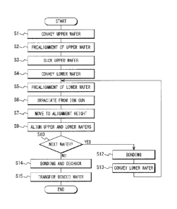
FIG. 12 shows the operation performed by
using the bonding unit 1. An operator first closes
the gate valve 5, and then sets the bonding chamber 2
to a vacuum atmosphere by using the vacuum pump 9 and
the load lock chamber 3 to an atmosphere with the
atmospheric pressure. The operator puts an upper-side
wafer on the upper-side cartridge 7 such that the
orientation flat of the upper-side wafer contacts the
wafer positioning pins 52-2 and 52-3 and the side of
the outer periphery of the upper-side wafer contacts
the wafer positioning pin 52-1. Moreover, the
operator puts the lower-side wafer on the lower-side
cartridge 8 such that the orientation flat of the
lower-side wafer contact the wafer positioning pins
62-2 and 62-3, and the side of the outer periphery of
the lower-side wafer contacts the wafer positioning
pin 62-1. A plurality of the lower-side cartridges 8
with the lower-side wafers are prepared. The operator
opens the lid of the load lock chamber 3, and arranges
the upper-side cartridge 7 in the load lock chamber 3
and arranges the plurality of lower-side cartridges 8
in the load lock chamber 3. Next, the operator closes
the lid of the load lock chamber 3 and sets the load
lock chamber 3 to the vacuum atmosphere.
The bonding unit control unit 10 opens the
gate valve 5 after the load lock chamber 3 is set to
CA 02758157 2011-10-06
- 32 -
the vacuum atmosphere. The bonding unit control unit
first controls the electrostatic chuck 18 to hold
the upper-side wafer. The bonding unit control unit
10 controls the conveyance mechanism 6 to convey the
5 upper-side cartridge 7 with the upper-side wafer put,
from the load lock chamber 3 to the stage cartridge
45. The bonding unit control unit 10 controls the
conveyance mechanism 6 to move down the hand 17 of the
conveyance mechanism 6. At this time, the upper-side
10 cartridge 7 is held by the stage cartridge 45 by
engaging the plurality of positioning holes 53-1 and
53-2 with the plurality of positioning pins 48-1 to
48-2 of the stage cartridge 45, respectively (Step
S1). The bonding unit control unit 10 controls the
conveyance mechanism 6 to draw back the hand 17 of the
conveyance mechanism 6 into the load lock chamber 3.
Next, the bonding unit control unit 10
controls the alignment mechanisms 91-1 and 91-2 to
pickup images of the alignment marks formed on the
upper-side wafer. The bonding unit control unit 10
controls the positioning mechanism 12 based on the
images such that the upper-side wafer is positioned in
the predetermined horizontal position (Step S2).
Next, the bonding unit control unit 10 controls the
pressure bonding mechanism 11 to move the
electrostatic chuck 18 down into the vertical
direction. The bonding unit control unit 10 controls
CA 02758157 2011-10-06
- 33 -
the pressure bonding mechanism 11 to stop the
electrostatic chuck 18 when the electrostatic chuck 18
contacts the upper-side wafer, and controls the
electrostatic chuck 18 to hold an upper-side wafer.
At this time, because the plurality of wafer
positioning pins 52-1 to 52-3 of the upper-side
cartridge 7 are formed not to protrude from the upper-
side wafer, the wafer positioning pins 52-1 to 52-3 of
the upper-side cartridge 7 do not contact the
electrostatic chuck 18. Therefore, the bonding unit 1
can make the electrostatic chuck 18 contact the upper-
side wafer more surely and can make the electrostatic
chuck 18 hold the upper-side wafer more surely. The
bonding unit control unit 10 controls the pressure
bonding mechanism 11 such that the upper-side wafer
leaves the upper-side cartridge 7, that is, the
electrostatic chuck 18 rise upwardly. The bonding
unit control unit 10 controls the conveyance mechanism
6 to draw back the upper-side cartridge 7 with no
upper-side wafer from the stage cartridge 45 into the
load lock chamber 3 after the upper-side wafer leaves
the upper-side cartridge 7 (Step S3).
The bonding unit control unit 10 controls the
conveyance mechanism 6 to convey the cartridge 8 with
the lower-side wafer put from the load lock chamber 3
to the stage cartridge 45 after the electrostatic
chuck 18 holds the upper-side wafer. The bonding unit
CA 02758157 2011-10-06
- 34 -
control unit 10 controls the conveyance mechanism 6 to
move down the hand 17 of the conveyance mechanism 6.
At this time, the lower-side cartridge 8 is held by
the stage cartridge 45 such that the plurality of
positioning holes 63-1 and 63-2 are engaged with the
plurality of positioning pins 48-1 and 48-2 of the
stage cartridge 45, respectively. The bonding unit
control unit 10 controls the conveyance mechanism 6 to
draw back the hand 17 of the conveyance mechanism 6
into the load lock chamber 3. Next, the bonding unit
control unit 10 closes the gate valve 5 and controls
the vacuum pump 9 to vacuum the bonding chamber 2 to
the bonding atmosphere with a predetermined vacuum
degree (Step S4).
Next, the bonding unit control unit 10
controls alignment mechanisms 91-1 and 91-2 to pick up
images of the alignment marks formed on the lower-side
wafer. The bonding unit control unit 10 controls the
positioning mechanism 12 based on the images to
position the lower-side wafer to a predetermined
horizontal position (Step S5). When the bonding
chamber 2 is set to the bonding atmosphere, the
bonding unit control unit 10 controls the ion gun 14
to emit particles for a space between the upper-side
wafer and the lower-side wafer in a state which the
upper-side wafer held by the electrostatic chuck 18 is
apart from the lower-side wafer held by the stage
CA 02758157 2011-10-06
- 35 -
cartridge 45 (Step S6). The particles are irradiated
to the upper-side wafer and the lower-side wafer to
remove oxide films formed on the surfaces and removes
impurities adhered to the surfaces.
The bonding unit control unit 10 controls the
pressure bonding mechanism 11 to move down the
electrostatic chuck 18 to a predetermined position
downwardly into the vertical direction. The bonding
unit control unit 10 controls the pressure bonding
mechanism 11 such that the upper-side wafer and the
lower-side wafer leave from each other by a
predetermined distance, that is, the electrostatic
chuck 18 stops at a predetermined position (Step S7).
Next, the bonding unit control unit 10 controls the
alignment mechanisms 91-1 and 91-2 such that the
images of the alignment marks formed on the upper-side
wafer and the alignment marks formed on the lower-side
wafer are picked up. The bonding unit control unit 10
controls the positioning mechanism 12 based on the
images of the upper-side wafer and the lower-side
wafer, so as to be bonded according to design (Step
S9).
After the upper-side wafer and the lower-side
wafer are bonded, when the bonded upper-side wafer
should be bonded with another lower-side wafer (Step
S10, YES), the bonding unit control unit 10 controls
the pressure bonding mechanism 11 such that the bonded
CA 02758157 2011-10-06
- 36 -
upper-side wafer contact the other lower-side wafer,
that is, the electrostatic chuck 18 moves down
downwardly into the vertical direction (Step S12).
The upper-side wafer and the lower-side wafer are
bonded through the contact of them and one sheet of
bonded wafer is generated. At this time, because the
plurality of wafer positioning pins 62-1 to 62-3 of
the lower-side cartridge 8 are formed not to protrude
from the lower-side wafer, the pins 62-1 to 62-3 do
not contact the electrostatic chuck 18 or the upper-
side wafer. Therefore, the bonding unit 1 can make
the upper-side wafer contact the lower-side wafer more
surely and can bond the upper-side wafer and the
lower-side wafer more surely. Moreover, at this time,
the island portions 61 of the lower-side cartridge 8
contact most of all the part of the lower-side wafer.
Therefore, the lower-side wafer can be prevented from
damage due to the load which is applied in the
bonding. Also, the bonding unit 1 can apply a larger
load on the upper-side wafer and the lower-side wafer.
The bonding unit control unit 10 controls the
electrostatic chuck 18 to leave the bonding wafer from
the lower-side cartridge 8, that is, to continue to
hold the bonded wafer, and controls the pressure
bonding mechanism 11 such that the electrostatic chuck
18 rises upwardly to the vertical direction. Next,
the bonding unit control unit 10 opens the gate valve
CA 02758157 2011-10-06
- 37 -
5, and controls the conveyance mechanism 6 to draw
back the lower-side cartridge 8 from the stage
cartridge 45 into the load lock chamber 3. After the
lower-side cartridge 8 with no bonded wafer is drawn
back into the load lock chamber 3, the bonding unit
control unit 10 controls the conveyance mechanism 6 to
convey the lower-side cartridge 8 with a lower-side
wafer from the load lock chamber 3 to the stage
cartridge 45. The bonding unit control unit 10
controls the conveyance mechanism 6 to move down the
hand 17 of the conveyance mechanism 6. At this time,
the plurality of positioning holes 63-1 and 63-2 are
engaged with the plurality of positioning pins 48-1 to
48-2 of the stage cartridge 45, respectively, so that
the lower-side cartridge 8 is held by the stage
cartridge 45. The bonding unit control unit 10
controls the conveyance mechanism 6 to draw back the
hand 17 of the conveyance mechanism 6 into the load
lock chamber 3. Next, the bonding unit control unit
10 closes the gate valve 5 and controls the vacuum
pump 9 to vacuum the bonding chamber 2 to the bonding
atmosphere with a predetermined vacuum degree (Step
S13).
Next, the bonding unit control unit 10
controls the alignment mechanisms 91-1 and 91-2 to
pick up images of the alignment marks formed on the
lower-side wafer. The bonding unit control unit 10
CA 02758157 2011-10-06
- 38 -
controls the positioning mechanism 12 based on the
images to position the lower-side wafer in a
predetermined horizontal position of (Step S5). When
the bonding atmosphere is generated inside the bonding
chamber 2, the bonding unit control unit 10 controls
the ion gun 14 to emit particles to a space between
the bonded wafer and the lower-side wafer in a state
that the bonded wafer held by the electrostatic chuck
18 is separated from the wafer held by the stage
cartridge 45 (Step S6). The particles are irradiated
to the bonded wafer and the lower-side wafer to remove
oxide films formed on the surfaces and remove
impurities adhered to the surfaces.
The bonding unit control unit 10 controls the
pressure bonding mechanism 11 to move down the
electrostatic chuck 18 to a predetermined position
downwardly into the vertical direction. The bonding
unit control unit 10 controls the pressure bonding
mechanism 11 such that the bonded wafer is separated
from the lower-side wafer by a predetermined distance,
that is, the electrostatic chuck 18 stops at a
predetermined position (Step S7). Next, the bonding
unit control unit 10 controls the alignment mechanisms
91-1 and 91-2 such that the images of the alignment
marks formed on the bonded wafer and the alignment
marks formed on the lower-side wafer are picked up.
The bonding unit control unit 10 controls the
CA 02758157 2011-10-06
- 39 -
positioning mechanism 12 based on the images of the
bonded wafer and the lower-side wafer so as to be
bonded according to the design (Step S9).
When another lower-side wafer is not bonded
after the bonded wafer and the lower-side wafer are
bonded (Step S10, NO), the bonding unit control unit
controls the pressure bonding mechanism 11 such
that the bonded wafer contacts the lower-side wafer,
that is, the electrostatic chuck 18 moves down
10 downwardly in the vertical direction. The bonded
wafer and the lower-side wafer are bonded through the
contact and one sheet of the bonded wafer is
generated. Moreover, the bonding unit control unit 10
controls the electrostatic chuck 18 to dechuck the
bonded wafer from the electrostatic chuck 18 (Step
S14).
According to such an operation, the bonded
wafer produced at step S12 can be more bonded with
another wafer without being taken out from the bonding
chamber 2. Therefore, according to such an operation,
three or more wafers can be bonded at higher speed as
compared with a case that a couple of wafers are
bonded, and three or more wafers can be bonded at a
low cost.
The bonding unit control unit 10 controls the
pressure bonding mechanism 11 to raise the
electrostatic chuck 18 upwardly in the vertical
CA 02758157 2011-10-06
- 40 -
direction. Next, the bonding unit control unit 10
opens the gate valve 5, and controls the conveyance
mechanism 6 to convey the cartridge 8 with the bonded
wafer put from the stage cartridge 45 to the load lock
chamber 3. The bonding unit control unit 10 closes
the gate valve 5 and controls the vacuum pump 4 to set
the load lock chamber 3 to atmosphere with an
atmospheric pressure. The operator opens the lid of
the load lock chamber 3 after the atmospheric-pressure
atmosphere is set inside the load lock chamber 3, and
takes out the bonded wafer (Step S15).
For example, when three wafers (wafers 82,
84, and 86) are bonded to one bonded wafer, the
operator prepares three cartridges (cartridges 81, 83,
and 85). The operator puts the wafer 82 on the
cartridge 81, puts the wafer 84 on the cartridge 83
and puts the wafer 86 on the cartridge 85. As the
cartridge 81, the upper-side cartridge 7 is
exemplified. As the cartridge 83, the lower-side
cartridge 8 is exemplified. As the cartridge 85, the
lower-side cartridge 8 is exemplified.
As shown in FIG. 13, after step Si is
executed, the cartridge 81 with the wafer 82 put is
set on the stage cartridge 45 and the electrostatic
chuck 18 absorbing nothing is arranged in a position
apart from the stage cartridge 45.
At step S3, as shown in FIG. 14, the wafer 82
CA 02758157 2011-10-06
- 41 -
put on the cartridge 81 which has been put on the
stage cartridge 45 contacts the electrostatic chuck 18
and the wafer 82 is sucked by the electrostatic chuck
18.
As shown in FIG. 15, after step S3 is
executed, the cartridge 81 with no wafer is put on the
stage cartridge 45 and the electrostatic chuck 18 on
which the wafer 82 has been sucked is arranged in a
position the stage cartridge 45.
As shown in FIG. 16, after step S4 is
executed, the cartridge 83 on which the wafer 84 is
put is put on the stage cartridge 45, and the
electrostatic chuck 18 by which the wafer 82 has been
absorbed is arranged in a position apart from the
stage cartridge 45.
As shown in FIG. 17, at step S12, the wafer
84 put on the cartridge 83 contacts the wafer 82
sucked by the electrostatic chuck 18.
As shown in FIG. 18, after step S12 is
executed, the bonded wafer 87 is formed from the wafer
84 and the wafer 82, and the cartridge 83 with no
wafer is put on the stage cartridge 45 nothing.
The electrostatic chuck 18 by which a bonded wafer 87
has been sucked is arranged in a position apart from
the stage cartridge 45.
As shown in FIG. 19, after step S13 is
executed, the cartridge 85 on which the wafer 86 has
CA 02758157 2011-10-06
- 42 -
been put is put on the stage cartridge 45 and the
electrostatic chuck 18 by which the bonded the wafer
87 has been sucked is arranged in a position apart
from the stage cartridge 45.
Because there is not another wafer to be
bonded after the wafer 86, step S14 is executed
without executing the step S12. As shown in FIG. 20,
at the step S14, the wafer 86 put on the cartridge 85
contacts the bonded wafer 87 sucked by the
electrostatic chuck 18.
As shown in FIG. 21, after step S14 is
executed, a bonded wafer 88 is formed from the bonded
wafer 87 and the wafer 86. The cartridge 85 on which
the bonded wafer 88 is put is located on the stage
cartridge 45. The electrostatic chuck 18 with no
wafer is arranged in a position apart from the stage
cartridge 45.
According to such an operation, the bonded
wafer 87 formed from the wafer 82 and the wafer 84 can
be bonded with the wafer 86 without being taken out
from the bonding chamber 2. Therefore, according to
such an operation, three or more wafers can be bonded
at higher speed compared with the case that a couple
of the wafers are bonded, and three or more wafers can
be bonded at the low cost.
The operation which is executed without using
the bonding unit 1 includes an operation of producing
CA 02758157 2011-10-06
- 43 -
a wafer which is a bonding object and an operation of
dicing the bonded wafer.
In the operation of producing the wafer as
the bonding object, the upper-side wafer and the
lower-side wafer are produced, e.g. the wafers 82, 84
and 86 shown in FIG. 13 to FIG. 21 are produced.
It should be noted that the bonded wafer
produced by bonding two wafers by using the bonding
unit 1 can be applied as the wafer 84 or the wafer 86.
Moreover, the wafer obtained by processing the bonded
wafer can be applied as the wafer 84 or the wafer 86.
If such a wafer is applied as the wafer 84 or the
wafer 86, The plurality of wafers can be bonded such
that an order where a plurality of bonding surfaces
are arranged and an order that the plurality of
bonding surfaces are bonded are different from each
other. Thus, it is possible to diversify in the form
of the bonding.
In the operation of dicing the bonded wafer,
the bonded wafer formed by using the bonding unit 1 is
divided into a plurality of devices. That is, the
operation which is executed by using the bonding unit
1 is suitable for producing the bonded wafer which is
divided into the plurality of devices.
A wafer 70 which is exemplified by the upper-
side wafer and the lower-side wafer is sometimes
transformed as shown in FIG. 22. When the wafer 70 is
CA 02758157 2011-10-06
- 44 -
put on a cartridge 71 which is exemplified by the
upper-side cartridge 7 and the lower-side cartridge 8,
a space 72 is formed between the wafer 70 and the
cartridge 71. The air filling the space 72 lifts the
wafer 70 and sometimes moves the wafer 70 along the
surface of the cartridge 71 if the atmosphere where
the wafer 70 and the cartridge 71 are arranged is
decompressed, when there is no passage which connects
the space 72 and the outside.
The gas filling the space between the upper-
side cartridge 7 and the upper-side wafer is exhausted
outside through passages between the plurality of
island portions 51-1 to 51-4. Such exhaustion
prevents the gas between the upper-side cartridge 7
and the upper-side wafer from lifting the upper-side
wafer and prevents the upper-side wafer from moving on
the upper-side cartridge 7. Moreover, the gas filling
the space between the lower-side cartridge 8 and the
lower-side wafer is exhausted outside through the
grooves 65 as passages. Such exhaustion prevents the
between the lower-side cartridge 8 and the lower-side
wafer from lifting the lower-side wafer and prevents
the lower-side wafer from moving on the lower-side
cartridge 8.
It should be noted that a multi-layer bonding
method of bonding according to the present invention
may be executed by using another bonding unit in which
CA 02758157 2011-10-06
- 45 -
the alignment mechanisms 91-1 and 91-2 are arranged in
other positions. The positions which are nearer to
the electrostatic chuck 18 than the positioning
mechanism 12, for example, the upper positions of the
electrostatic chuck 18 are exemplified. The multi-
layer bonding method of according to the present
invention can bond three or more wafers at higher
speed even when being applied to such a bonding unit,
like the above embodiments.
It should be noted that in the other
embodiment of the multi-layer bonding method according
to the present invention, steps S2, S5, S7 and S9 in
the embodiments are omitted. Such a multi-layer
bonding method can be applied when high accuracy
alignment is unnecessary. Like the embodiments, three
or more wafers can be bonded at higher speed and at a
low cost.
It should be noted that in the multi-layer
bonding method according to another embodiment of the
present invention, the conveyance mechanism 6 in the
above embodiments directly contacts and conveys the
wafer and the stage cartridge 45 directly contacts the
wafer and holds the wafer. In such a multi-layer
bonding method, three or more wafers can be bonded at
higher speed, like the above embodiments. Moreover,
in such a multi-layer bonding method, the recovery of
the cartridge is unnecessary. Three or more wafers
CA 02758157 2011-10-06
- 46 -
can be bonded at higher speed, as compared with the
above embodiments. Moreover, in such a multi-layer
bonding method, the cartridge is unnecessary and three
or more wafers can be bonded at the low cost.
It should be noted that in the multi-layer
bonding method according to another embodiment of the
present invention, a plurality of wafers are stacked
downwardly in a vertical direction. According to such
a multi-layer bonding method, the wafer conveyed into
the bonding chamber 2 by the conveyance mechanism 6 is
transferred to the electrostatic chuck 2 in the air
without being supported by the stage cartridge 45 and
is held by the electrostatic chuck 2. Next, the wafer
held by the electrostatic chuck 2 is bonded by another
wafer supported on the stage cartridge 45. When the
bonded wafer is supported on the stage cartridge 45,
still another wafer is held by the electrostatic chuck
2 in the same way and the bonded wafer and the wafer
held by the electrostatic chuck 2 are bonded. In such
a multi-layer bonding method, three or more wafers can
be bonded at a low cost, like the multi-layer bonding
method in the above embodiment. However, it is
difficult transfer a wafer from the conveyance
mechanism 6 to the electrostatic chuck 2 in the air,
and the control by being handed over is very difficult
and becomes labile operation. Therefore, in the
multi-layer bonding method in the above embodiment, a
CA 02758157 2014-04-09
52313-16
- 47 -
plurality of wafers are stacked on the upper side.
Three or more wafers can be bonded more stably,
compared with a multi-layer bonding method in which a
plurality of wafers are laminated on the lower side.
It should be noted that the multi-layer
bonding method according to the present invention can
be applied to another bonding unit in which two wafers
are brought into contact and bonded by moving the
wafers into a direction which is different from the
vertical direction. As the direction, a horizontal
direction is exemplified. In the multi-layer bonding
method according to the present invention, three or
more wafers can be bonded at a higher speed when being
applied to such a bonding unit, like the above
embodiments.
This patent application claims a priority
based on Japanese Patent Application NO. 2009-247855
filed on October 28, 2009.