Note: Descriptions are shown in the official language in which they were submitted.
CA 02758376 2011-10-07
WO 2010/119248 PCT/GB2010/000747
Security Document
Field of the Invention
The present invention relates to improvements in security documents and
in particular to such documents incorporating piezochromic materials as
security
features.
Background to the Invention
Security documents such as banknotes now frequently carry optically
variable devices that exhibit an angularly dependent coloured reflection. This
has
been motivated by the progress in the fields of computer-based desktop
publishing and scanning, which renders conventional security print
technologies
such as intaglio and offset printing more prone to attempts to replicate or
mimic. It
is well known in the prior art to use liquid crystal materials or thin film
interference
structures to generate such angularly dependent coloured reflection. Examples
of
liquid crystal based security devices are described in EP0435029, W003061980,
and EP1156934 and examples of security devices utilising thin film
interference
structures are described in US4186943 and US20050029800.
The planar nature of liquid crystal films and thin film interference
structures results in the observed angularly dependent coloured reflection
exhibiting limited spatial variation for. example a simple red to green colour
change on tilting the security device away from normal incidence.
Photonic crystals are structured optical materials in which the refractive
index varies periodically in two or preferably three dimensions. These
materials
exhibit a range of interesting optical effects when subject to electromagnetic
radiation of a wavelength comparable to the spatial modulation of the
refractive
index. Bragg reflection may occur over a range of wavelengths that depend on
the direction of incidence/propagation and the periodicity of refractive index
variation. This gives rise to photonic 'energy gaps' that are analogous to the
electronic band gaps in semiconductors. Typically, electromagnetic waves
within
a certain frequency range cannot propagate in particular directions within the
crystal, and incident electromagnetic radiation at these wavelengths is
1
CA 02758376 2011-10-07
WO 2010/119248 PCT/GB2010/000747
consequently reflected. It is the presence of such partial photonic band gaps
that
gives rise to the shimmering colours observed in opal gemstones.
In general there is a complex dependence on the wavelength, direction of
propagation and polarisation that dictates which electromagnetic waves may
propagate within the photonic crystal and those that are otherwise reflected.
However, if the modulation in refractive index is sufficiently strong,
propagation of
certain frequencies can be forbidden for any crystalline direction, and a
complete
photonic band gap arises. In this case light is prevented from propagating
within
the crystal in any direction, and the material acts as an ideal reflector such
that all
light of a wavelength within the band gap range is perfectly reflected
irrespective
of the incident direction.
There exists two well-documented methods of fabricating structures with
the necessary highly ordered variation in refractive index - microfabrication
and
self-assembly. Due to the complexity of microfabrication considerable effort
has
been devoted to investigating self-assembling systems comprised of submicron
three-dimensional arrays of dielectric spheres. Such photonic crystals are
formed
by allowing a colloidal suspension of identically sized spheres to settle
slowly
under the influence of gravity or by the application of an external force such
that
the spheres are encouraged to order. One example is the fabrication of
synthetic
opal structures where uniformly sized sub-micron silica spheres are organised
through a sedimentation process into a face-centred cubic crystal structure.
Further enhancements to this technique have been developed such that
the synthetic opal acts as a precursor or template to further customise the
structure. It has been shown that it is possible to use such systems as
templates
to realise materials known as inverse or inverted opals. Here, the regions
between the silica spheres are first filled with a suitable matrix material,
and the
silica is then dissolved by chemical means to give a system that consists of
an
array of air spheres or voids surrounded by a uniform matrix.
The optical properties of photonic crystals can be engineered and varied
to a greater extent than the optical properties of planar liquid crystal and
thin film
interference devices. Firstly the angular and wavelength dependence of the
reflected light can be more easily controlled by varying the crystal lattice
structure
by either simply adjusting the sphere size, or the sphere. separation.
Similarly,
2
CA 02758376 2011-10-07
WO 2010/119248 PCT/GB2010/000747
selected allowed and disallowed reflections/transmissions may be engineered or
enhanced by introducing structural defects into the lattice or by introducing
nanoparticles into the structure. This in principle gives freedom to modify
and
engineer the band structure and hence the wavelength and spatial dependence
of the reflectivity.
The use of photonic crystals in security devices is known from the prior art
and examples include W003062900, US20050228072 W02008017869,
W02008017864, W02008098339 and EP1972463. Furthermore the interactive
nature of such materials has been documented in a paper "Interactive Elastic
Photonic Crystals", A.C. Arsenault et al, presented at the conference "Optical
Document Security", San Francisco, 23-25 January 2008. The challenge for the
use of photonic crystals in security devices is how to incorporate such
devices
into security documents such that the additional optical effects possible from
photonic crystals, compared to other well known dichroic materials, can be
used
to validate the document. The object of the current invention is to improve
the
security of the devices described in the prior art and provide a practical
solution to
the problem of how to use these and other similar materials as authenticating
devices.
Summary of the Invention
In accordance with the invention we provide a security document
comprising:-
a security device attached to a first part of the document, the security
device comprising a region of piezochromic material; and,
a contact structure attached to a second part of the document, different
from the first part, the contact structure exhibiting relief;
wherein the security document is adapted to allow the security device to
be pressed against the contact structure; and,
wherein the piezochromic material is arranged such that, when the
security device and contact structure are. pressed together, an optical effect
is
generated within the piezochromic material.
The present invention provides a two-part self-authenticating security
device in a document, in which an optical effect is generated in a
piezochromic
3
CA 02758376 2011-10-07
WO 2010/119248 PCT/GB2010/000747
material by pressing it against a contact structure positioned in a different
part of
the document to the region of piezochromic material.
A piezochromic material is here defined as any material that changes
colour on the application of a deformation. Much of the discussion herein is
focussed upon photonic crystals as examples of piezochromic materials. One
class of alternative piezochromic materials to photonic crystal materials is
liquid
crystal materials. French patent application FR2698390 provides examples of
cholesteric and nematic liquid crystal materials that change colour under the
application of a pressure. Alternatively it is also known that in lyotropic
liquid
crystal materials it is possible to produce colour changes by the application
of
pressure to disturb the layers of crystals and thereby alter their
transmission
characteristics.
The contact structure can be formed by a number of different processes
and typically exhibits relief as a raised or textured surface. This may be
formed by
a printing process such as with intaglio printing, or by embossing.
Furthermore, a
relatively hard material having a relief profile may simply be mounted to the
document. In a further example, a watermark can be used as the contact
structure. Watermarks in fibrous substrates exhibit a variation in relief due
to the
variation in the number of fibres present in different regions of the
watermark. We
have found that although the relief in a conventional multitonal banknote
watermark cannot be felt by touch the relief caused by the variation in fibre
volume are sufficient to generate an optical effect in a photonic crystal. A
watermark therefore may act as a contact structure in that the change in
relief is
as a result of the difference in the number of fibres across the watermark.
This is
different from an intaglio embossed structure where the thickness of the
substrate
actual remains substantially constant but its position is caused to be
modulated
with respect to a line defining a plane prior to the embossing being
performed.
The variation in the number of fibres provides the watermark with a variable
optical density enabling the pattern to be viewed in transmitted light unlike
a
conventional blind embossed structure (one without inking) which is not
viewable
in transmitted light.
It will also be appreciated that in some cases the relief may be caused by
a local reduction in the surface height (analogous to electrotype watermarks)
and
therefore below the height of the surrounding material. However, the presence
of
4
CA 02758376 2011-10-07
WO 2010/119248 PCT/GB2010/000747
projecting regions (of a height in excess of the surrounding material) may be
more convenient to fabricate.
The optical effect may comprise a first optical effect in a region of
deformation of the photonic crystal and a second optical effect in a region
which
is not deformed. One or each may be optically variable effects. The optical
effect
may therefore represent a change in colour. The term "colour" is intended to
include white/mirrored (essentially reflecting at all relevant wavelengths),
black
(essentially absorbing at all relevant wavelengths) and wavelengths outside
the
human-visible range. Typically the colour is a human-visible colour The
optical
effect also may represent a change to or from complete reflection regardless
of
wavelength. Furthermore, one or each optical effect may be invisible to the
human eye and therefore may exhibit their effects in the ultra-violet or infra-
red
regions of the electromagnetic spectrum. In general the optical effect is
representative of the relief of the contact structure although this is not
essential.
Thus if the relief is formed as an image, then the optical effect in the
photonic
crystal may be a similar or complementary image. Thus the optical effect may
reproduce the image. If the relief within the contact structure is on a fine
scale
then the optical effect may simply represent more general features of the
relief
such as its lateral scale or regions in which the relief height changes most
severely.
Preferably, at least part of the document is arranged to be flexible so as to
allow the first and second parts to be brought together. Indeed the entire
document may be formed from a flexible substrate. It is contemplated that
parts
of the document may also be relatively inflexible and therefore a hinge or
fold
may be provided to aid in bringing the first and second parts together.
Whilst the first and second parts may be in the material of the document
itself, typically the first and second parts comprise respective first and
second
surfaces of the document, these being a common surface in some cases.
One or each of security device and contact structure may comprise a
cover layer, which is typically a thin layer and which may serve to protect
the
material beneath.
With or without presence of the cover layer, the action of the pressing
together of the region of piezochromic material and the contact structure
typically
causes a temporary distortion within the structure of the piezochromic
material.
5
CA 02758376 2011-10-07
WO 2010/119248 PCT/GB2010/000747
Such a distortion may last for a fraction of a second upon removal of the
applied
stress, or may last for minutes or even hours.
The security device may further comprise an absorbing layer mounted to
the region of piezochromic material. This may act as the cover layer. The
absorbing layer is therefore typically dark in appearance. It is preferably a
non-
selectively absorbing material. It may be a pigmented ink or a non-pigmented
absorbing dye. Instead of, or in addition to the absorbing layer, the
structure of
the piezochromic material itself may be provided with absorbing regions which,
like the absorbing layer, increase the contrast of any optical effect
observable.
In an alternative embodiment the contact structure itself can act as the
absorbing layer (by containing an absorbing phase) for example the contact
structure may take the form of a darkly coloured raised intaglio printed
image.
Regardless of the contact structure used, the security device may further
comprise a printed ink layer having a colour which is substantially the same
as at
least one of: the colour of the relief structure, the colour of light
reflected from the
piezochromic material when in a stressed state or the colour of light
reflected
from the piezochromic material when in an unstressed state.
Two or more contact structures may be provided and they may be used
together to generate an image as part of the optical effect. For example a
first
part of a composite image may be represented in a first of the plurality of
contact
structures and a second part of the composite image may be represented in a
second of the plurality of contact structures. The first and second image
parts
may form a resultant image when combined. If each contact structure is
positioned to cause corresponding deformation of the piezochromic material
during compression then the resultant image may be visible when the device is
compressed. Notably the contact structures may be positioned upon opposing
sides of the document. One such structure may also be formed as part of the
region of piezochromic material or attached thereto.
A number of different types of photonic crystal may be used to implement
the invention as piezochromic materials. They may include nanoparticles
distributed homogeneously, inhomogeneously in regions, or as a concentration
gradient.
The region of piezochromic material may be provided in a number of
forms, for example as a self-supporting layer. Alternatively, it may be
supported
6
CA 02758376 2011-10-07
WO 2010/119248 PCT/GB2010/000747
by a substrate or carrier layer to which it is mounted directly or indirectly
(through
one or more further layers). The substrate or the carrier layer may take the
form
of a polymeric layer. The piezochromic material may also take the form of a
pigmented coating or layer where the piezochromic material is in the form of a
pigment.
It is also preferred that the device is arranged to be machine-readable.
This may be achieved in a number of ways. For example the change in
wavelength of the reflected light with change in direction of incident light
could be
used for machine authentication. In a further example at least one layer of
the
device (optionally as a separate layer) or the region of piezochromic material
itself may further comprise machine-readable material. Preferably the machine-
readable material is a magnetic material, such as magnetite. The machine-
readable material may be responsive to an external stimulus. Furthermore, when
the machine-readable material is formed into a layer, this layer may be
transparent.
The region of piezochromic material may be located within the document
such that it has a first face on a first side of the document and a second
face on
an opposing side of the document. Thus the region of piezochromic material may
adopt a through-thickness arrangement. The region of piezochromic material may
be mounted to a window in the document or may actually function as the window.
Thus it is preferred that the region of piezochromic material is formed as a
film for use in the security document. The security documents include
banknotes,
cheques, passports, identity cards, certificates of authenticity, fiscal
stamps and
other documents for securing value or personal identity.
The security device may take various different forms for use with security
documents, these including a security thread, a security fibre, a security
patch, a
security strip, a security stripe, a security foil or a security coating or
printed layer
as non-limiting examples.
When a photonic crystal material is used, this may be based on an inverse
opal structure or an opal structure. The 'sponge-like' nature of the inverse
opal
structure allows it to be more readily compressed and therefore more suitable
for
the current invention. Compressing such a material distorts the periodicity of
the
structure and consequently can affect a change in the visual appearance. This
7
CA 02758376 2011-10-07
WO 2010/119248 PCT/GB2010/000747
may be assisted by the use of an elastomeric matrix material, which
naturally gives a more flexible system.
Suitable materials for use in inverse opal structures are disclosed in
W02008098339. The inverse opal film can be generated using a template, in one
example the template is formed by using self-assembly techniques to order
spheres on a glass substrate. The spheres may be inorganic for example silica
or
polymeric for example polystyrene. The voids between the spheres are then
filled with a polymer material. Examples of suitable polymer materials are
listed in
W02008098339 and include a monomer or pre- polymer selected from the group
consisting of methacrylic acid esters, acrylic acid esters, polyisoprene,
polybutadiene, polyurethane precursors, crosslinkable polyethers, and mixtures
thereof. The spheres are then removed by an appropriate etchant or solvent
depending on the type of sphere material used. In the case of polystyrene the
spheres are dissolved by an appropriate solvent to give a system that consists
of
an array of air spheres or voids surrounded by a uniform matrix. More
information
on the selection of an appropriate solvent to dissolve polymer microspheres
can
be found in "An Introduction to Polymer Colloids", 1st Edition, published by
Springer in December 1989.
If the inverse opal structures are to be used as a pigment in a coating or
printing ink then the film can be converted into a pigment for example by
detaching the film from the substrate and breaking the film up to the desired
particle size.
The photonic crystal security device may also contain regions comprising
both standard opal structures and inverse opal structures. Both structures
exhibit
the phenomenon known as structural colour whereby their visual appearance is a
function of their configuration; in particular the arrangement, size and
refractive
index (relative to the matrix) of the spheres or voids.
The regions composed of an inverse structure will show greater optical
variability as a function of deformation compared to those composed of a
standard opal-like structure. This may be assisted by the use of an
elastomeric
matrix material, which naturally gives a more flexible system.
One further advantage of such a feature is the possibility of deriving one
region (the inverse opal) from the other (the opal). This will involve post-
8
CA 02758376 2011-10-07
WO 2010/119248 PCT/GB2010/000747
processing a continuous opal-like structure, for example using the techniques
discussed earlier, to convert a selected region to an inverse opal-like
structure. In
other words, a security device could be made by `patterning' and converting
regions of standard opal-like structure to ultimately give two types of
crystal
structure.
In practice, most inverse opal-like structures are achieved by first
fabricating a standard opal and then selectively removing the submicron
spheres
by a selective etching process that leaves the matrix material unaffected. If
a
security device were made form a suitable material system it would be possible
to
etch out the spheres in chosen regions whilst leaving other areas unaltered.
The
resultant feature would have a continuous matrix. For example one way of
producing such a device would be to follow the method described above for the
inverse opal structure but then only dissolve the spheres in localised regions
to
give a material that in a first region consists of air spheres separated by a
uniform
matrix of the polymeric material and in a second region consists of
polystyrene
spheres surrounded by the uniform matrix of the polymeric material.
Brief Description of the Drawings
Some examples of a document according to the invention are now described,
with reference to the accompanying drawings, in which:-
Figure 1 is a side view of a first example document;
Figure 2 is a plan view of the first example;
Figure 3 is a side view showing the document when folded;
Figure 4 illustrates the image generated within the photonic crystal;
Figure 5 shows a second example, partly in section, in an open configuration;
and,
Figure 6 shows the second example in a partially closed configuration.
Description of Examples
In the example described below a security document in the form of a
banknote is provided with a "self-authenticating" security feature using the
combination of a contact structure and a photonic crystal.
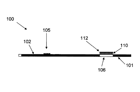
Referring to Figure 1, the banknote is illustrated at 100 and in this
example is formed from a paper-based material which acts as a substrate 101.
Conventional materials can be used to produce the substrate 101, including
9
CA 02758376 2011-10-07
WO 2010/119248 PCT/GB2010/000747
plastics materials. The banknote 100 is generally flexible due to the material
from
which it is made, and it being arranged to have a thin cross section. This
allows
the banknote 100 to be folded repeatedly. The banknote 100 should be
understood to contain a number of optional security features including
security
threads, specialised printing inks and techniques and so on. These are not
illustrated in Figure 1 for simplicity of explanation only. A first face 102
is shown
facing towards the top of Figure 1. At a position approximately one quarter of
the
way along the length of the banknote 100 from one edge and on the first face,
an
area of intaglio printing is located forming a contact structure 105. As will
be
appreciated by those in the art, a feature of intaglio printing is that can be
used to
produce an area of printing ink positioned upon the substrate, the area
printed
having an ink height of typically 5 to 50 micrometres above the surrounding
substrate surface. The intaglio printing may take the form of an image and may
be printed using opaque or transparent inks. In the present case an opaque ink
is
used. The intaglio printing forming the contact structure on the face 102 of
the
banknote 100 provides a localised area of surface relief.
An optical window 106 is located at a position approximately three
quarters of the distance along the length of the banknote 100. The window 106
is
formed from a transparent plastics material and is integral with the banknote
substrate 101. Windows in banknotes are known in the art and typically allow
an
observer to look through the banknote, as a security feature. For example,
W08300659 describes a polymer banknote formed from a transparent substrate
comprising an opacifying coating on both sides of the substrate. The
opacifying
coating is omitted in localised regions on both sides of the substrate to form
a
transparent region. EP1 141480 describes a method of making a transparent
region in a paper substrate. Other methods for forming transparent regions in
paper substrates are described in EP0723501, EP0724519, EP1398174 and
W003054297. The opposing side of the banknote 100 forms a second face 108.
Figure 2 shows the second face of the banknote 100 when viewed in plan. The
window can be seen to take the form of an ellipse although other shapes are of
course contemplated.
Referring once more to Figure 1, a photonic crystal 110 (which is a
piezochromic material) is bonded to the surface of the window 106 on the first
face 102 side of the banknote 100. The photonic crystal 110 takes the form of
a
CA 02758376 2011-10-07
WO 2010/119248 PCT/GB2010/000747
film of a thickness of under 200 micrometres, preferably less than 50
micrometres
and even more preferably less than 30 micrometres. The use of a film is
advantageous in that, since it is thin, it is relatively easy to distort the
photonic
structure and therefore to produce an optical effect. A further discussion of
suitable materials can be found in a paper "Interactive Elastic Photonic
Crystals",
A.C. Arsenault et al, presented at the conference "Optical Document Security",
San Francisco, 23-25 January 2008. In a further example the photonic crystal
can
be applied as a coating or printing over the window 106.
The outer surface of the photonic crystal film 110 is covered by an
absorbing layer 112. In the present case this is a non-selectively reflecting
ink
and is therefore of very dark appearance. This layer 112 is thin so as to
maximize
the optical effect which results within the crystal. The absorbing layer
serves a
dual function. Firstly, it assists in providing contrast to ease in the
observation of
any optical effect within the photonic crystal film 110. Secondly, the
absorbing
layer 112 acts to an extent as a protective coating.
Because the use of a covering absorbing layer may not be aesthetically
pleasing or compatible with the design of the banknote and in an alternative
embodiment the intaglio printed image can itself act as the absorbing layer
and
this is achieved by using a darkly coloured intaglio image.
The self-authenticating security feature of the present example is provided
by the combination of the contact structure 105 and the photonic crystal film
110.
Figure 3 shows how the flexibility of the substrate allows the region of the
banknote 100 containing the window and photonic crystal layer to be folded
onto
the intaglio print of the contact structure 105. Once in the position shown in
Figure 3, the absorbing layer 112 and photonic crystal film 110 can be pressed
against the surface relief of the intaglio print of the contact structure 105.
The
compression force, which is experienced by these components as a compressive
stress, is illustrated by the arrows 115.
The intaglio print is therefore forced into the absorbing layer 112 which
deforms. Additionally the photonic crystal film beneath the absorbing layer is
also
deformed, this causing a change in the optical properties of the photonic
crystal
layer in the deformed regions when compared with the non-deformed regions of
the crystal. The regions of deformation conform to the surface relief of the
intaglio
print.
11
CA 02758376 2011-10-07
WO 2010/119248 PCT/GB2010/000747
Upon releasing the compressive force and separating the absorbing layer
112 from the intaglio print, the photonic crystal film may or may not return
to its
former undistorted configuration. This is dependent upon the material used to
form the photonic crystal film. Furthermore, the speed of any relaxation to
its
original configuration is also a function of the material.
In any deformed region the deformation of the photonic crystal causes a
local optical effect which is different to the optical effect present in a non-
deformed region. One or each of these optical effects may be an optically
variable effect such as a colour shift, or may be an effect such as total
reflection
at all wavelengths.
In the present case by way of example, the non-deformed region might
exhibit a red colour effect, whereas that of the deformed region might exhibit
a
green effect, each according to white light illumination. These effects are
reflective effects and are observable through the window 106 when the second
face 108 of the banknote 100 is illuminated. The absorbing layer 112 provides
a
black backing to enhance the visible effect of the photonic crystal film. In
the
regions where the intaglio print image is imprinted into the photonic crystal
film,
causing local distortion, the image becomes visible as a green image through
the
window 106 due to the contrast between the deformed and non-deformed
regions.
An example of this is illustrated in Figure 4, where a non-deformed region
120 of the photonic crystal film provides a plain background to the image of
the
intaglio print formed in the photonic crystal as shown at 121.
A strong optical contrast is generated when the folded surfaces are
pressed between two hard planar surfaces such as two glass plates. If a
material
with a long relaxation time (the time to return to an non-deformed state) is
chosen, such as a time of several seconds to a few minutes, then the glass
plates
can be removed and the image in the photonic crystal film viewed through the
window 106. However, if a short relaxation time typically one second or less
is
chosen, then the image 121 may only be visible through the glass plate which
contacts the window 106 on the second face 102 whilst the pressure is applied.
In summary of the above example the security feature is authenticated by
folding the note over and pressing the photonic crystal against an area on the
banknote that has a raised or textured surface. If very short relaxation times
are
12
CA 02758376 2011-10-07
WO 2010/119248 PCT/GB2010/000747
used then the viewing window should be placed against a rigid clear surface to
facilitate applying pressure from the rear of the note. One
practical/manufacturing advantage of the having a self authentication
structure is
that it can avoid the problems associated with adhering the photonic crystal
to an
uneven surface. Durability is consequently better and the longevity is
improved.
The example described above is viewed primarily in reflection. The optical
effects of the photonic crystal material are best visualised against the dark
non-
selectively absorbing background provided by the absorbing layer 112 under the
photonic crystal layer.
In the alternative embodiment where there is no additional dark absorbing
film but the intaglio printed image is in a dark absorbing colour then the
film in its
uncompressed state will be uniformly opalescent but on pressing the photonic
crystal film against the intaglio surface the areas in contact with the dark
intaglio
print will appear in a different colour to the background regions not in
contact with
the background print and furthermore the contrast between the two regions will
be striking due to the increased intensity of the compressed region resulting
from
the fact that it is now being observed against an absorbing background layer.
A similar result to the presence of an absorbing layer may be achieved by
the introduction of absorbing particles into the photonic crystal material. If
using
absorbing particles, the absorbing particles should be significantly greater
than
the size of the spheres of the photonic lattice such that they do not cause a
change in the lattice and consequently an undesirable change in the optical
properties.
Whilst the use of a black, or very dark, substantially totally absorbing layer
may give rise to the most strong colourshifts, other effects may be generated
by
the use of a partially absorbing layer of other colours or a combination of
colours,
giving rise to differing apparent colourshift colours. If the absorbing layer
is
present, this may be overprinted or coated with an effect ink to make it more
aesthetically pleasing when viewed from the first face 102.
The optical properties of the photonic crystal may also be additionally or
alternatively further modified or enhanced by the use of nanoparticles
positioned
within the crystal structure, preferably at interstitial sites. The
nanoparticles may
13
CA 02758376 2011-10-07
WO 2010/119248 PCT/GB2010/000747
be distributed substantially uniformly through the crystal such that each part
of
the crystal exhibits substantially the same optical effect. Alternatively the
nanoparticles may be distributed inhomogeneously through the crystal such that
different parts of the crystal exhibit a substantially different optical
effect. Thus the
nanoparticles may be distributed according to a concentration gradient. The
nanoparticles may also be distributed in a number of regions having different
concentrations.
A particularly advantageous feature of the current invention is that the
compressible photonic crystal film can be used to reveal hidden images on a
secure document having contact structures created by blind embossing or raised
transparent inks. In a further example it would be possible to have areas of
transparent raised image printed over a substantially planar coloured area.
The
coloured area (preferably printed by litho-printing) acts to obscure the
presence of
the raised image, but when the photonic crystal is pressed against that area
the
surface relief is revealed in the photonic crystal. Preferably the
substantially
planar coloured area will be darkly coloured and can therefore also function
as
the absorbing layer.
In the banknote example given above the photonic crystal film undergoes
a colour change and therefore a visible-to-visible transition. Other
contemplated
examples include a switch from one visible colour to another on deformation, a
switch from invisible to coloured or from reflecting UV to being transparent
to UV
such that on being distorted a UV feature may be activated underneath the
photonic crystal film.
Ideally, this feature would work best with an inverse opal photonic crystal
structure, which are known from W02008098339. However, a noticeable effect
may be achieved with a standard opal structure (such as described in
US20040131799, US20050228072, US20040253443 and US6337131) if
sufficient lattice distortion can be achieved, or if deformable spheres are
used.
In addition to using an image which is raised above the surface such as an
embossing or intaglio printed image it has also been realised that a watermark
produces a similar effect when a suitable photonic crystal film is pressed
against
it.
The use of watermarks is fairly common in many security documents. High
security multi-tonal watermarks are typically created using a cylinder mould
14
CA 02758376 2011-10-07
WO 2010/119248 PCT/GB2010/000747
process and are formed by varying the volume of paper fibres so that in some
regions the volume of fibres increases, and in others decreases relative to
that of
the base paper layer which surrounds the watermark region. When viewed in
transmitted light the regions with few fibres are lighter and the regions with
increased fibres are darker than the base paper, and the contrasts can be seen
very clearly. Different types of watermarks have different advantages. A multi-
tonal watermark is often a pictorial image, such as a portrait, and can be
very
detailed and complex which significantly reduces the risk of counterfeiting.
In cylinder-mould papermaking, paper is formed on a partially submerged
wire-cloth covered mould cylinder, which rotates in a vat containing a dilute
suspension of paper fibres. As the mould cylinder rotates, water is drawn
through
the wire cloth depositing fibres onto the cylinder surface. When the wire
cloth is
embossed with a detailed image, the fibres deposit with a lesser or greater
thickness on the raised and sunken elements of the embossing to form a fully
three-dimensional watermark in the finished paper.
The variation in paper thickness in the final watermark is a result of fibre
movement from the raised regions of the embossed mesh to the sunken regions
of the embossed mesh as the water is drawn through the wire cloth. The fibre
movement, and therefore the tonal variation in the watermark, is governed by
the
drainage rate and that is dependent on the profile of the embossing. This
enables excellent control in the gradation of the watermark pattern, producing
a
subtle tonal range that is unique to the cylinder mould-made watermark
process.
An alternative process for generating uniform light tonal regions (and
providing enhanced watermark security) is the electrotype process. In the
electrotype process a thin piece of metal, generally in the form of an image
or
letter, is applied to the wire cloth of the cylinder mould cover, by sewing or
welding, creating a significant decrease in drainage and fibre deposition and
thereby forming a light watermark in the paper. An electrotype watermark may
be
lighter than a watermark generated, and produced, by conventional embossing.
This electrotyping process is known in papermaking and has been described in
US-B-1901049 and US-B-2009185.
An electrotype watermark is therefore an area of paper having just a
uniform decrease in paper thickness. The area is typically quite small and the
change in paper thickness quite distinct so as to create a very light image,
usually
lighter than areas within a pictorial watermark.
CA 02758376 2011-10-07
WO 2010/119248 PCT/GB2010/000747
Such an effect can be partly mimicked by the counterfeiter by using
"transparentising" resins, UV lacquers applied locally or even cooking oil.
However, there is a significant problem arising from the use of large thinner
areas
both in respect of weakening the paper and its poor security.
The advantage of watermarks is that whilst they conventionally provide a
security feature visible in transmitted light, they can also be used to
provide a
latent security feature visible in reflected lighted when a compressible
photonic
crystal film is pressed onto the watermark region. Counterfeiters attempt to
mimic
watermarks by printing with variable density inks or by using transparentising
resins, UV lacquers applied locally or cooking oil. However this only
replicates the
effect in transmitted light and will not replicate the effect observed when
combined with a compressible photonic crystal film, and therefore the use of a
watermark with a piezochromic material region provides further potential
protection for a secure document comprising a watermark.
In the case of the use of a watermark, as for other relief structures the
light
may comprise visible and/or non-visible light, therefore including for example
ultraviolet and infra-red light. Broad or narrow wavelength bands may be used.
Likewise, the photonic crystal may be arranged to selectively reflect light in
the
non-visible part of the spectrum (including ultra-violet and infra-red).
A second example document is now described in association with Figures
5 and 6. In this case the security document is a booklet in the form of a
passport
200. This is illustrated in Figure 5 where the passport is shown in an open
configuration, partly in section. The passport 200 has an outer cover 201 and
internal pages 202,203 formed from a paper material. The pages are separated
by a foldable region in the form a hinge 204. One of a number of known methods
used in bookbinding may be used to produce the hinge 204. A watermark 205 is
located within the structure of the paper of page 202, this watermark being
formed by one of the methods described above and containing at least one
region of reduced or modulated thickness. The watermark 205 operates in the
conventional manner in that it provides a security feature in respect of light
transmitted through the watermark. On page 203, a photonic crystal security
device 210 is provided, this containing a photonic crystal which is positioned
such
that when the hinge 204 is operated so as to bring the surfaces of the pages
202
and 203 together, the surface of the photonic crystal security device contacts
the
16
CA 02758376 2011-10-07
WO 2010/119248 PCT/GB2010/000747
watermark. This is illustrated in Figure 6 where the page positions represent
a
partially closed configuration since the cover 201 of the passport remains
open.
When a user applies a compressive stress as indicated by the arrows 215 (using
their fingers or by compressing the pages between two rigid flat objects), the
local
density and/or thickness variations in the watermark 205 produce a
corresponding deformation in the photonic crystal. This results in any image
present within the watermark being represented as an optical effect in the
photonic crystal of the device 210.
In the present case the photonic crystal film comprises carbon
nanoparticles which enhance resonant scattering events that occur within the
photonic crystal giving rise to strong structural colours and removes the
requirement for an absorbing layer. The photonic crystal in this case is
arranged
to relax over a period of 1-2 minutes, thus allowing time for the passport
pages
202,203 to be returned to the open position indicated in Figure 5. A person
examining the document then has plenty of time to view the watermark 205 on
page 202 in transmission (for example by viewing a light source through the
watermark). In addition the photonic crystal security device 210 can be
inspected
for the existence of a reversed (mirrored) image of the watermark image.
Note that with the use of a watermark the local thickness of the paper may
be less than that of the surrounding paper forming the page 202. Taking this
to
the extreme the watermark may be replaced with a perforation, i.e. a region of
zero thickness. The perforations can be introduced into the paper during the
papermaking process by preventing fibre deposition in localised areas by
blinding
or sealing the cylinder mould cover. Alternatively a paper or polymer
substrate
can be perforated in a subsequent secondary process, for example by laser
cutting or mechanical punching.
In a further example, the photonic crystal may be embedded within the
paper of the page 203 such that it does not project above the plane defined by
the page surface. It may of course also be arranged to lie below such a plane.
The use of a watermark as a contact structure, coupled with the use of a
photonic crystal security device, provides a significant additional security
feature
for use in security documents.
17
CA 02758376 2011-10-07
WO 2010/119248 PCT/GB2010/000747
Alternatively the distortion in the piezochromic material in any of the
examples may be permanent and this would be particularly useful in security
devices which only need to be validated once for example as a tamper evident
security device.
It will be appreciated that each of the arrangements discussed herein
provide a self-authenticating function upon the security document and also
significant technological hurdle to overcome for prospective counterfeiters.
18