Note: Descriptions are shown in the official language in which they were submitted.
CA 02758633 2011-10-13
WO 2010/119240
PCT/GB2010/000734
- 1 -
OPTICAL WAVEGUIDE AND DISPLAY DEVICE
This invention relates to an optical waveguide and a display device. In
particular it is relevant to display devices in which image bearing light is
injected
into a waveguide, is expanded in two orthogonal dimensions to form a visible
image and is released from the waveguide.
A prior art device of this type is shown in US6509529. In that device a
slab waveguide contains three separate differently-oriented diffraction
gratings,
one to inject the light into the waveguide, a second to expand it in a first
dimension, and a third to expand it in a second dimension and to release the
thereby-formed image from the waveguide. Whilst this arrangement is simpler
than earlier proposals in which the third grating is in a separate waveguide
from
the first two, it still poses manufacturing challenges in that the three
differently-
oriented gratings (whether produced holographically or a surface-relief
gratings)
still must be very accurately aligned relative to each other if good results
are to
be achieved.
The present invention seeks to alleviate these difficulties by offering a
solution which can be implemented using fewer diffraction gratings.
According to an aspect of the invention an optical waveguide in which in
operation light propagates by total internal reflection comprises a grating
structure having three diffraction regions, a first diffraction region being
for
diffracting image-bearing light into the waveguide, a second diffraction
region
being for further diffracting the image-bearing light so as to expand it in a
first
dimension and a third diffraction region being for further diffracting the
image-
bearing light so as to expand it in a second dimension and for releasing it
from
the waveguide as a visible image, wherein at least two of said diffraction
regions have aligned gratings and at least one reflecting surface is provided
which reflects light received from one of said at least two diffraction
regions
back to the other of said at least two diffraction regions for a further
diffraction.
The at least two aligned diffraction regions may have gratings with
uniform orientation and/or spatial frequency, although the structure of the
grating may vary. For example, the first diffraction region and the second
CONFIRMATION COPY
CA 02758633 2011-10-13
WO 2010/119240
PCT/GB2010/000734
- 2 -
diffraction region may have uniform orientation and/or spatial frequency, but
the
fringes of the first region may be higher than those of the second region.
A said reflecting surface may be perpendicular to two parallel surfaces of
the waveguide between which light propagates within the waveguide parallel to
those surfaces by total internal reflection.
A said reflecting surface may be an edge surface of the waveguide.
Alternatively or in addition a said reflecting surface may be embedded
within the waveguide.
A said reflecting surface may have an optical coating whereby to control
the reflectance of the surface and/or to control the planarization of light
reflected
therefrom.
In a first embodiment a said reflecting surface may be positioned to
receive image-bearing light which has been expanded in the first dimension by
diffraction by the second diffraction region and to reflect it back to the
grating
structure for further diffraction by the third diffraction region to expand it
in the
second dimension.
In a second embodiment a said reflecting surface may be positioned to
receive light which has been diffracted into the waveguide by the first
diffraction
region and to reflect it back to the grating structure for diffraction by the
second
diffraction region to expand it in the first dimension.
The second and third diffraction regions may comprise identically-
oriented gratings which respectively diffract the light to expand it in the
first and
second dimensions.
Alternatively or in addition the second and the third diffraction regions
may comprise identically oriented gratings which respectively diffract the
light
into the waveguide and expand it in the first dimension.
In both of these embodiments, the use of a reflecting surface enables
identically-oriented gratings to be used for light-injection and for expansion
in
the first dimension, and alternatively or in addition for expansion in the
first and
CA 02758633 2016-10-20
26158-304
- 3 -
second dimensions. Thus it is possible to use no more than two (and preferably
only
one) grating orientations for all diffraction operations within the waveguide.
Consequently, at least two of the gratings within the waveguide can be
formed as a single grating, different parts of which are used for different
diffraction
operations. Alternatively they can be formed as two or three discrete
gratings, all
having the same orientation. Because their orientations are the same they
effectively
can be formed in one manufacturing operation, and thus the likelihood of
angular
misalignment is much reduced. We include such discrete but identical gratings
within
the term "single grating" in this specification.
When identically-orientated gratings are used for only two of the three
diffraction functions, the other function may be effected by a further
grating. In one of
the foregoing embodiments that function is the injection of image-bearing
light into
the waveguide. In the other it is the expansion of the light in the second
dimension
and its release from the waveguide a visible image.
The waveguide of the invention may be employed in a variety of display
devices including but not limited to helmet-mounted displays, head-mounted
displays
(e.g. spectacles or goggles) or head-up displays e.g. for aircraft or other
vehicles.
According to another aspect of the invention, there is provided an
optical waveguide in which in operation light propagates by total internal
reflection,
comprising: two parallel surfaces between which light propagates within the
waveguide parallel to those surfaces by total internal reflection; a grating
structure
having three diffraction regions, a first diffraction region being for
diffracting image-
bearing light into the waveguide, a second diffraction region being for
further
diffracting the image-bearing light so as to expand it in a first dimension
and a third
diffraction region being for further diffracting the image-bearing light so as
to expand
it in a second dimension and for releasing it from the waveguide as a visible
image,
wherein at least two of said diffraction regions have aligned gratings; and at
least one
reflecting edge surface which reflects light received from one of said at
least two
CA 02758633 2016-10-20
26158-304
- 3a -
diffraction regions back to the other of said at least two diffraction regions
for a further
diffraction, the reflecting edge surface being perpendicular to the two
parallel
surfaces of the waveguide.
According to another aspect of the invention, there is provided a
helmet-mounted, head-mounted, head-up or other display device comprising the
optical waveguide above.
The invention now will be described merely by way of example with
reference to the accompanying drawings wherein;
Figure 1 (taken from the aforementioned US6580529) shows a prior art
apparatus, and
Figures 2, 3 and 4 show three embodiments of the present invention.
Referring to Figure 1, a prior art slab waveguide 10 incorporates three
separate differently-oriented gratings H1, Hz, H3. Image-bearing light 12 is
incident in
the Z-direction on grating H1, the grooves or other diffracting structure of
which is
oriented in the y-direction. The grating turns the light through 90 , which
then
propagates between the parallel faces 14, 16 of the waveguide in the x-
direction. The
light then encounters grating H2, the
CA 02758633 2011-10-13
WO 2010/119240
PCT/GB2010/000734
- 4 -
diffracting structure of which is oriented at 450 to the x and y directions.
This
grating expands the image-bearing light in the x-dimension, turns it though
900
into the y direction and presents it to the grating H3, the diffracting
structure of
which is oriented in the x-direction. The grating expands the light in the y-
dimension and releases in the z-direction as a two-dimensional image 18
visible
to a observer. The preferred embodiments of the present invention now to be
described achieve the same functionality in an alternative way.
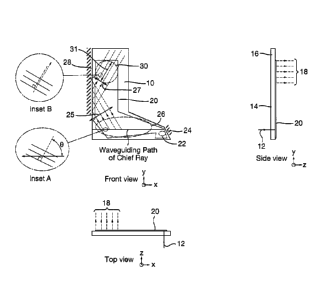
In Figure 2, a slab waveguide 10 of BK7 glass again has parallel
principal surfaces 14, 16 between which waveguide (propagation) of light takes
place. It however comprises a single grating 20 of uniform orientation (the
grooves are inclined at 30 degrees to the x-axis) and spatial frequency
(groove
pitch d=435nm) throughout, and which with the assistance of two specular
reflecting surfaces delivers a visible image.
Collimated image bearing light 12 is incident normally on a first input
portion, or region, 22 of the grating 20 and is diffracted within it through
90 so
as to propagate by total internal reflection through the waveguide to an edge
surface 24 of the waveguide. This surface is planar and perpendicular to the
principal surfaces 14, 16 and is inclined to the y-axis of the slab at an
angle a .
The surface 24 is polished and metallised to form a specular reflector. The
angle a is chosen (here it is 30 ) so that the propagating light incident upon
it is
reflected with its chief ray then propagating along the x-axis of the
waveguide.
The light in the incident at an angle 8 on a second or turning portion, or
region,
26 of the grating 20. This area of the grating, whilst having the same
orientation
and spatial frequency as the area 22, is optically coated so as to have a low
diffraction efficiency (between 5% and 30%). The light rays are thus partially
diffracted, leading to pupil expansion of the image-bearing light in a first
dimension, shown at 25 in figure 2. The diffracted rays are directed by the
grating so as to propagate through the waveguide to a second edge surface 28.
This edge surface, also perpendicular to the principal planes 14, 16, is
polished
and metallised similarly to edge surface 24 to form a second specular
reflector.
Light incident upon it is reflected towards a third or output part, or region,
30 of
the grating 20. The light rays are incident on the second part 26 of the
grating
CA 02758633 2011-10-13
WO 2010/119240
PCT/GB2010/000734
- 5 -
so that the chief ray makes an angle 0 of 60 to the normal to the grating
orientation (the direction of the grooves) as shown at insert A of Figure 2.
The
subsequent reflection of the diffracted rays at surface 28 results in the
reflected
chief ray (now having a reflected first expansion dimension 27) propagating
through the waveguide and being incident normally on the output part 30 of the
grating, as shown at insert B, that is, the reflected chief ray makes an angle
of
,0 with the normal to the groove direction of the grating region 30. This
part of
the grating also is coated so as to have a low diffraction efficiency of 10% -
20%, and the rays are thus partially diffracted out of the waveguide resulting
in
pupil replication (expansion) in a second dimension 31 orthogonal to the
reflected first dimension 27. The resulting emerging light is visible as a
image
to an observer.
Thus, in this embodiment, a single grating achieves
- image injection into the waveguides
pupil replication within the waveguide in one dimension
- pupil replication within the waveguide in a second dimension
diffraction of the expanded pupil image to the user's eye.
The embodiments of Figures 3 and 4 are generally similar to that of
Figure 2, so only the differences will be described. Corresponding parts have
the same reference numerals.
In the embodiment of Figure 3, the input part 22 of the grating 20 is
replaced by a separate grating 32, the grooves of which are disposed parallel
to the y-axis. This diffracts the incoming image-bearing light 12 directly to
the
turning part 26 of the grating 20; the reflecting surface 24 is not required.
The
image-bearing light otherwise propagates through the waveguide 10 in the
same way as described with reference to figure 2, and so presents a visible
image to an observer.
Thus in the embodiment one grating is used for image injection into the
waveguide, and the other is used for
pupil replication within the waveguide in one dimension
CA 02758633 2011-10-13
WO 2010/119240
PCT/GB2010/000734
-6-
- pupil replication within the waveguide in a second dimension
- diffraction of the expended pupil image to the user's eye.
In Figure 4, the grating 20 is again provided with input 22 and turning 26
parts, and reflecting surface 24 is retained. However it is at a different
angle to
surface 24 of Figure 2, being disposed instead parallel to the y-axis of the
slab
10. The orientation of the grating 20 also is different, the grooves thereof
being
inclined at an angle of 600 to the x-axis so that image-bearing light incident
on
the input part 22 is diffracted and propagated to the reflective surface 24
and
thence reflected so that the chief ray propagates and is incident on the
grooves
of the turning region at 30 (i.e. at 8=60 to the normal to the grooves,
inset A).
The light is partially diffracted and expanded in a first dimension (here
the x-dimension) and propagates through the waveguide to a second low
diffraction efficiency (10%-20%) grating 34 having its orientation (grooves)
lying
in the x-direction. The diffracted rays are incident normally on this grating
(inset
B) and are partially diffracted out of the waveguide, the partial diffraction
expanding the pupil in a second dimension, here the y-dimension.
Thus a visible image is again presented to the observer.
In this embodiment, one grating is used for
image injection into the waveguide
pupil replication within the waveguide in one dimension
- diffraction of the image-bearing light towards the second grating.
The second grating is used for
pupil replication within the waveguide in the second dimension
diffraction of the expanded pupil image to the users' eye.
In all embodiments of the invention the gratings 20, 32, 45 may be
formed by any convenient conventional means, e.g. by physically removing
material or by holography. The reflective surfaces 24, 28 may be optically
coated to control this reflectance and/or the polarisation state of the
reflected
CA 02758633 2016-10-20
26158-304
- 7 -
light. They may also be embedded reflective surfaces rather than exposed
edges, e.g. if necessary to protect them.
The reflective surfaces 24, 28 may be optically coated to control their
reflectance and/or the polarisation state of the reflected light.
The groove spacing d of the grating 20 is chosen according to known
principles to optimise the display response and will depend on the required
field
of view, the refractive index of the waveguide and the wavelength of the
light.
The abstract of the disclosure is repeated here as part of the specification.
In a slab waveguide which expands an image-bearing pupil into a visible
image, reflective edge surfaces are used to redirect once-diffracted light
back
through the same grating structure. The number of separate grating structures
thereby can be reduced to two or even one, compared to three in the prior art.
=