Note: Descriptions are shown in the official language in which they were submitted.
CA 02759074 2011-10-17 110275-WO-00:910429
DESCRIPTION
TITLE OF THE INVENTION
Method for Manufacturing Silicon Carbide Substrate
TECHNICAL FIELD
The present invention relates to a method for manufacturing a silicon carbide
substrate.
BACKGROUND ART
An SiC (silicon carbide) substrate has recently increasingly been adopted as a
semiconductor substrate used for manufacturing a semiconductor device. SiC has
a
band gap wider than Si (silicon) that has been used more commonly. Therefore,
a
semiconductor device including an SiC substrate is advantageous in a high
breakdown
voltage, a low ON resistance and less lowering in characteristics in an
environment at a
high temperature.
In order to efficiently manufacture a semiconductor device, a substrate is
required to have a size not smaller than a certain size. According to US
Patent No.
7,314,520 (Patent Document 1), an SiC substrate not smaller than 76 mm (3
inches) can
be manufactured.
PRIOR ART DOCUMENT
PATENT DOCUMENT
Patent Document 1: US Patent No. 7,314,520
SUMMARY OF THE INVENTION
PROBLEMS TO BE SOLVED BY THE INVENTION
Industrially, the size of an SiC single crystal substrate is still limited to
approximately 100 mm (4 inches). Accordingly, semiconductor devices cannot be
efficiently manufactured using large single crystal substrates,
disadvantageously. This
disadvantage becomes particularly serious in the case of using the property of
a plane
other than the (0001) plane in SiC of hexagonal system. Hereinafter, this will
be
-1-
CA 02759074 2011-10-17 110275-WO-00:910429
described.
An SiC single crystal substrate small in defect is usually manufactured by
slicing
an SiC ingot obtained by growth in the (0001) plane, which is less likely to
cause
stacking fault. Hence, a single crystal substrate having a plane orientation
other than
the (0001) plane is obtained by slicing the ingot not in parallel with its
grown surface.
This makes it difficult to sufficiently ensure the size of the single crystal
substrate, or
many portions in the ingot cannot be used effectively. For this reason, it is
particularly
difficult to effectively manufacture a semiconductor device that employs a
plane other
than the (0001) plane of SiC.
Instead of increasing the size of such an SiC single crystal substrate with
difficulty, it is considered to use a silicon carbide substrate having a
supporting portion
and a plurality of small single crystal substrates connected thereon. The size
of the
silicon carbide substrate can be made larger by increasing the number of
single crystal
substrates as required. However, in the case where such a supporting portion
and
single crystal substrate are connected, the strength of the connection may be
insufficient.
The present invention was made in view of the above-described problem, and an
object of the present invention is to provide a method for manufacturing a
silicon
carbide substrate that can have the connecting strength between a single
crystal
substrate and a supporting portion increased.
MEANS FOR SOLVING THE PROBLEMS
A method according to the present invention for manufacturing a silicon
carbide
substrate includes the following steps.
At least one single crystal substrate, each having a backside surface and made
of
silicon carbide, and a supporting portion having a main surface and made of
silicon
carbide, are prepared. In the preparing step, at least one of the backside
surface and
main surface is formed by machining. By this forming step, a surface layer
having
distortion in the crystal structure is formed on at least one of the backside
surface and
main surface. The surface layer is removed at least partially. Following this
removal,
-2-
CA 02759074 2011-10-17 110275-WO-00:910429
the backside surface and main surface are connected to each other.
According to the present invention, the connecting strength between the
backside surface and main surface can be increased by removing the surface
layer having
distortion.
Preferably, the step of removing the surface layer at least partially is
carried out
by sublimation of the surface layer. Accordingly, the surface layer can be
readily
removed at least partially while avoiding additional occurrence of distortion
in the
crystal structure. More preferably, in the step of preparing at least one
single crystal
substrate and a supporting portion, a surface layer is formed at the backside
surface, and
in the step of removing the surface layer at least partially, the surface
layer formed at the
backside surface is removed at least partially. Accordingly, the surface layer
formed at
the backside surface of at least one single crystal substrate can be removed
partially.
Further preferably, in the step of removing the surface layer at least
partially, the
backside surface and main surface are arranged to face each other prior to
sublimation
of the surface layer. Accordingly, since the backside surface and main surface
are
already facing each other at the point of time when the surface layer is
removed,
subsequent connection therebetween is facilitated.
The step of removing the surface layer at least partially may be carried out
by
sacrificial oxidation. The step of removing the surface layer at least
partially may be
carried out chemically.
Preferably, the step of removing the surface layer at least partially is
carried out
such that the surface layer is removed entirely. Accordingly, the connecting
strength
between the backside surface and main surface can be further improved.
Preferably, the step of connecting the backside surface and the main surface
to
each other is carried out by causing sublimation of silicon carbide from the
main surface
and recrystallization of silicon carbide on the backside surface, between the
backside
surface and main surface. In the case where the step of removing the surface
layer at
least partially is carried out by sublimation of the surface layer, both the
removing step
-3-
CA 02759074 2011-10-17 110275-WO-00:910429
and connecting step can be carried out by means of sublimation. Further, in
the case
where the backside surface and main surface are arranged to face each other
prior to
sublimation of the surface layer in the step of removing the surface layer at
least partially,
the backside surface and main surface can be connected to each other by just
changing
the direction of mass transfer through sublimation, after the surface layer is
sublimed.
Moreover, in the case where the surface layer is present, not only on the
backside
surface, but also on the main surface, the surface layer on the main surface
can be
eliminated by the sublimation in the step of connecting the backside surface
and main
surface to each other.
Preferably, at least one single crystal substrate includes a plurality of
single
crystal substrates. Accordingly, a silicon carbide substrate having a large
area can be
obtained.
The step of removing the surface layer at least partially set forth above may
be
carried out by etching the surface layer. This etching includes, for example,
wet
etching or gas etching.
In the step of preparing at least one single crystal substrate, the backside
surface
may be polished mechanically. Accordingly, the backside surface can be
rendered flat.
Further, the thickness of the surface layer formed on the backside surface can
be
reduced.
In the step of preparing at least one single crystal substrate, the backside
surface
may be formed by slicing. In other words, the backside surface is a surface
formed by
slicing, and not polished thereafter. Accordingly, there are irregularities on
the
backside surface. In the case where the supporting portion is provided by
sublimation
on the backside surface, the space in the depression of the irregularities can
be used as a
cavity where sublimation gas spreads.
Preferably, at least one single crystal substrate includes a first single
substrate
having a first surface opposite to the backside surface. The first surface has
an off
angle greater than or equal to 50 and less than or equal to 65 relative to
the {0001 }
-4-
CA 02759074 2011-10-17 110275-WO-00:910429
plane. Accordingly, the channel mobility at the first surface can be increased
as
compared to the case where the first plane is the {0001 } plane.
More preferably, the angle between the off orientation of the first surface
and the
<I-100> direction of the first single crystal substrate is less than or equal
to 5 .
Further preferably, the off angle of the first surface relative to the {03-38}
plane in the
<1-100> direction of the first single crystal substrate is greater than or
equal to - 3 and
less than or equal to 5 .
EFFECT OF THE INVENTION
As apparent from the description set forth above, the connecting intensity
between a single crystal substrate and a supporting portion can be increased
according
to a method for manufacturing a silicon carbide substrate of the present
invention.
BRIEF DESCRIPTION OF THE DRAWINGS
Fig. I is a plan view schematically showing a configuration of a silicon
carbide
substrate in a first embodiment of the present invention.
Fig. 2 is a schematic sectional view taken along line II-11 in Fig. 1.
Fig. 3 is a sectional view schematically showing a first step in a method for
manufacturing a silicon carbide substrate in the first embodiment of the
present invention.
Fig. 4 is a partial enlarged view of Fig. 3.
Fig. 5 is a partial sectional view schematically showing a mass transfer
direction
through sublimation in a second step of the method for manufacturing a silicon
carbide
substrate in the first embodiment of the present invention.
Fig. 6 is a partial sectional view schematically showing a mass transfer
direction
through sublimation in a third step of the method for manufacturing a silicon
carbide
substrate in the first embodiment of the present invention.
Fig. 7 is a partial sectional view schematically showing a cavity transfer
direction
through sublimation in the third step of the method for manufacturing a
silicon carbide
substrate in the first embodiment of the present invention.
Fig. 8 is a partial sectional view schematically showing a void transfer
direction
-5-
CA 02759074 2011-10-17 110275-WO-00:910429
through sublimation in the second step of the method for manufacturing a
silicon carbide
substrate in the first embodiment of the present invention.
Fig. 9 is a sectional view schematically showing a configuration of a single
crystal substrate in a first step of a method for manufacturing a silicon
carbide substrate
in a second embodiment of the present invention.
Fig. 10 is a sectional view schematically showing a configuration of a
supporting
portion in the first step of a method for manufacturing a silicon carbide
substrate in a
second embodiment of the present invention.
Fig. 11 is a sectional view schematically showing one step in the method for
manufacturing a silicon carbide substrate in a second embodiment of the
present
invention.
Fig. 12 is a sectional view schematically showing a configuration of a silicon
carbide substrate in a third embodiment of the present invention.
Fig. 13 is a sectional view schematically showing a configuration of a silicon
carbide substrate in a fourth embodiment of the present invention.
Fig. 14 is a partial sectional view schematically showing a configuration of a
semiconductor device in a fifth embodiment of the present invention.
Fig. 15 is a schematic flowchart of a method for manufacturing a semiconductor
device in the fifth embodiment of the present invention.
Fig. 16 is a partial sectional view schematically showing a first step in the
method for manufacturing a semiconductor device in the fifth embodiment of the
present
invention.
Fig. 17 is a partial sectional view schematically showing a second step in the
method for manufacturing a semiconductor device in the fifth embodiment of the
present
invention.
Fig. 18 is a partial sectional view schematically showing a third step in the
method for manufacturing a semiconductor device in the fifth embodiment of the
present
invention.
-6-
CA 02759074 2011-10-17 110275-WO-00:910429
Fig. 19 is a partial sectional view schematically showing a fourth step in the
method for manufacturing a semiconductor device in the fifth embodiment of the
present
invention.
MODES FOR CARRYING OUT THE INVENTION
Embodiments of the present invention will be described hereinafter based on
the
drawings.
(First Embodiment)
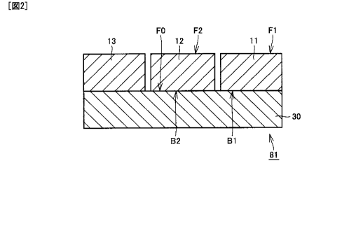
Referring to Figs. I and 2, a silicon carbide substrate 81 of the present
embodiment includes a supporting portion 30, and single crystal substrates 11-
13.
Supporting portion 30 is a layer made of silicon carbide, and the layer has a
main surface
FO. Single crystal substrates 1 1 -19 are made of silicon carbide, arranged in
a matrix,
as shown in Fig. 1. The backside surface of each of single crystal substrates
11-19 and
main surface FO of supporting portion 30 are connected to each other. For
example,
single crystal substrate 11 (first single crystal substrate) includes a
surface F1 (first
surface) and a backside surface B 1 (first backside surface) opposite to each
other.
Single crystal substrate 12 has a surface F2 (second surface) and a backside
surface B2
(second backside surface) opposite to each other. Each of backside surfaces B
I and
B2 is connected to main surface FO.
The surface of each of single crystal substrates 11-19 preferably has a plane
orientation {03-38}. As the plane orientation, {0001 }, { 11-20} or { I-100}
can be
employed. Further, a plane offset by several degrees from each of the
aforementioned
plane orientation can also be used.
A method for manufacturing silicon carbide substrate 81 will be described
hereinafter. Although only single crystal substrates 11 and 12 among single
crystal
substrates 11-19 are mentioned for the sake of simplification in the following
description,
single crystal substrates 13-19 follow the description of single crystal
substrates 11 and
12. The same applies to the description in other embodiments.
Referring to Figs. 3 and 4, there are provided a supporting portion 30, single
-7-
CA 02759074 2011-10-17 110275-WO-00:910429
crystal substrates 11-19 (generically refer to as "single crystal substrate
group 10"), and
a heating device. At this stage, supporting portion 30 is not necessarily in
the form of
single crystal, and may take the form of polycrystal or sintered compact.
The heating device includes first and second heat bodies 91 and 92, a heat-
insulating container 40, a heater 50, and a heater power source 150. Heat-
insulating
container 40 is made of a material of high heat resistance. Heater 50 is, for
example,
an electrical resistance heater. First and second heat bodies 91 and 92 are
capable of
heating supporting portion 30 and single crystal substrate group 10 by
reradiation of the
heat obtained by absorbing the emitted heat from heater 50. First and second
heat
bodies 91 and 92 are made of graphite, for example, having low porosity.
First heat body 91, single crystal substrate group 10, supporting portion 30,
and
second heat body 92 are arranged so as to be stacked in the cited order.
Specifically,
single crystal substrates 11-19 are arranged in a matrix on first heat body
91.
Supporting portion 30 is placed on the surface of single crystal substrate
group 10.
Then, second heat body 92 is placed on supporting portion 30. The stacked
first heat
body 91, single crystal substrate group 10, supporting portion 30 and second
heat body
92 are accommodated in heat-insulating container 40 in which heater 50 is
provided.
The atmosphere in heat-insulating container 40 is obtained by reducing the
atmospheric pressure. The pressure of the atmosphere is preferably set higher
than
10-' Pa and lower than 104 Pa.
The aforementioned atmosphere may be inert gas atmosphere. For inert gas,
noble gas such as He or Ar, nitrogen gas, or mixed gas of the noble gas and
nitrogen gas
can be used, for example. In the case where mixed gas is employed, the ratio
of the
nitrogen gas is 60%, for example. The pressure in the processing chamber is
preferably
less than or equal to 50 kPa, more preferably less than or equal to 10 kPa.
Referring to Fig. 5, a surface layer 71 (Fig. 5) is formed on the backside
surface
of single crystal substrate group 10 (Fig. 3) prepared as set forth above. For
example,
surface layer 71 is formed on each of backside surfaces B 1 and B2. In the
preparing
8-
CA 02759074 2011-10-17 110275-WO-00:910429
step of single crystal substrates 11 and 12, surface layer 71 is a layer
having distortion in
the crystal structure, formed at backside surfaces B 1 and B2 by machining
thereof. For
example, in the case where single crystal substrates 11-19 are produced by
being sliced
from a bulk of silicon carbide single crystal, the surface layer is produced
by this slicing.
The surface layer produced by slicing has a thickness of approximately 20 m,
for
example. In the case where mechanical polishing is applied to backside
surfaces B I
and B subsequent to slicing, the relatively thick surface layer caused by
slicing can be
removed. However, a relatively thin surface layer will be produced by this
mechanical
polishing.
It is to be noted that supporting portion 30 is just situated on each of
single
crystal substrates 11 and 12, and not connected. Therefore, a minute cavity GQ
is
present between each of back surfaces B I and B2 and supporting portion 30.
Therefore, surface layer 71 is facing cavity GQ.
By heater 50, single crystal substrate group 10 including single crystal
substrates
11 and 12, and supporting portion 30 are heated by first and second heat
bodies 91 and
92, respectively, up to a temperature corresponding to a level at which
sublimation
recrystallization reaction occurs. This heating is first carried out to cause
a
temperature difference such that the temperature of single crystal substrate
group 10 is
higher than the temperature of supporting portion 30. Namely, a temperature
gradient
is produced such that the temperature becomes lower in the upward direction in
the
drawing. This temperature gradient is preferably greater than or equal to 1
C/cm and
less than or equal to 100 C/cm, more preferably greater than or equal to 10
C/cm and
less than or equal 50 C/cm, between single crystal substrate group 10 and
supporting
portion 30.
As described above, when the temperature of each of single crystal substrates
11
and 12 is set higher than the temperature of supporting portion 30, mass
transfer occurs
by sublimation in cavity GQ, as indicated by arrow MI in the drawing. As a
result,
surface layer 71 is removed at least partially, preferably entirely. The
sublimated
-9-
CA 02759074 2011-10-17 110275-WO-00:910429
silicon carbide is recrystallized on main surface FO of supporting portion 30
to be
absorbed thereby.
Referring to Fig. 6, the temperature of supporting portion 30 is set higher
than
the temperature of each of single crystal substrates 11 and 12. Specifically,
a
temperature gradient is produced such that the temperature becomes lower in
the
downward direction in the drawing. In other words, the direction of the
temperature
gradient is inverted. This temperature gradient is preferably greater than or
equal to I
C/cm and less than or equal to 200 C/cm, more preferably greater than or
equal to 10
C/cm and less than or equal to 50 C/cm, between single crystal substrate
group 10 and
supporting portion 30. By such a temperature gradient, mass transfer by
sublimation
occurs in cavity GQ, as indicated by arrow M2 in the drawing.
Referring to Fig. 7, the mass transfer indicated by arrow M2 in Fig. 5
corresponds, conversely, to the hollow shift indicated by arrow H2 in Fig. 7,
in
association with the hollow present in cavity GQ. There is a great in-plane
variation in
the height of cavity GQ (the dimension in the vertical direction in the
drawing). This
variation causes a great in-plane variation in the rate of the hollow shift
corresponding
to cavity GQ (arrow H2 in the drawing).
Referring to Fig. 8, the hollow corresponding to cavity GQ (Fig. 7) cannot be
shifted while maintaining its shape due to the aforementioned variation, and
is instead
decomposed into a plurality of voids VD (Fig. 7). As a result, each of single
crystal
substrates 11 and 12 is connected to supporting portion 30.
As the heating progresses, void VD moves away from main surface FO, as
indicated by arrow H3. Accordingly, the connecting strength is further
increased.
Moreover, the crystal structure of supporting portion 30 gradually changes to
that
corresponding to the crystal structure of single crystal substrate group 10
from the
region closer to single crystal substrate group 10. Thus, a silicon carbide
substrate 81
is obtained.
According to the present embodiment, surface layer 71 (Fig. 5) is removed, not
- 10-
CA 02759074 2011-10-17 110275-WO-00:910429
mechanically, but by sublimation. By this removal, surface layer 71 having
distortion
can be removed while avoiding additional occurrence of distortion in the
crystal
structure at backside surfaces BI and B2. Thus, the connecting strength can be
increased between each of backside surfaces B 1 and B2 and main surface FO.
Furthermore, surface layer 71 can be removed by a simple step of heat
processing.
Moreover, increase in the electrical resistance in the thickness direction
(vertical
direction in Fig. 2) caused by the crystal defect at surface layer 71 can be
suppressed.
Prior to sublimation of surface layer 71, backside surfaces BI and B2 are
arranged to face main surface FO, as shown in Fig. 5. Accordingly, the
subsequent
step of connecting each of backside surfaces B 1 and B2 to main surface FO
(Figs. 6-8)
can be facilitated since the surfaces are already facing each other at the
point of time
surface layer 71 is removed.
Moreover, the step of removing surface layer 71 and the step of connecting
each
of backside surfaces B 1 and B2 to main surface FO are both carried out by
sublimation.
Specifically, the two steps can be carried out by just inverting the
temperature gradient
for the sublimation and recrystallization. Accordingly, the manufacturing step
of
silicon carbide substrate 81 can be simplified.
Since sublimation from main surface FO occurs, as shown in Fig. 6, in the
connection of each of backside surfaces B 1 and B2 to main surface FO, the
surface layer,
if present on main surface FO, will be removed. Accordingly, adverse influence
of the
surface layer on the connecting strength can be avoided.
Since surfaces F1 and F2 (Fig. 2) are provided, the surface area of silicon
carbide
substrate 81 can be increased as compared to the case where only surface F1 is
provided.
Preferably, each of single crystal substrates I 1-19 has a crystal structure
of the
4H polytype. Thus, a silicon carbide substrate 81 suitable for manufacturing a
semiconductor directed to electric power use can be obtained.
Preferably, in order to prevent silicon carbide substrate 81 from cracking,
the
difference between the thermal expansion coefficient of supporting portion 30
and the
-11-
CA 02759074 2011-10-17 110275-WO-00:910429
thermal expansion coefficient of single crystal substrates 1 I-19 in silicon
carbide
substrate 81 is made as small as possible. Accordingly, occurrence of a
warpage at
silicon carbide substrate 81 can be suppressed. To this end, the crystal
structure of
supporting portion 30 is to be identical to that of single crystal substrates
11-19.
Specifically, the crystal structure of supporting portion 30 is made to match
that of
single crystal substrates 11-19 by sufficient mass transfer (Fig. 8: arrow H3)
through
sublimation and recrystallization.
Preferably, the in-plane variation in the thickness of each of supporting
portion
30 and single crystal substrate group 10 (Fig. 4) prepared prior to the heat
treatment is
set as small as possible. For example, this variation is set less than or
equal to 10 m.
For the purpose of suppressing in-plane variation, a flattening process, for
example, is to
be carried out.
Preferably, the electrical resistivity of supporting portion 30 prepared prior
to the
heat treatment is set less than 50 mQ-cm, more preferably, less than 10 mf cm.
Preferably, the impurity concentration in supporting portion 30 of silicon
carbide
substrate 81 is set greater than or equal to 5 x 1018cm 3, more preferably
greater than or
equal to I X 1020cm 3. By manufacturing a vertical type semiconductor device
conducting a current flow vertically such as a vertical type MOSFET (Metal
Oxide
Semiconductor Field Effect Transistor) using such silicon carbide substrate
81, the ON
resistance of the vertical semiconductor device can be reduced.
Preferably, the average value of the electrical resistivity of silicon carbide
substrate 81 is set less than or equal to 5 mQ=cm, more preferably less than
or equal to 1
mS2=cm.
Preferably, the thickness of silicon carbide substrate 81 (dimension in the
vertical
direction in Fig. 2) is greater than or equal to 300 m.
Preferably, surface F 1 has an off angle greater than or equal to 50 and less
than
or equal to 650 relative to the (0001) plane. Accordingly, the channel
mobility at
surface F I can be increased as compared to the case where surface F 1 is the
{ 0001)
-12-
CA 02759074 2011-10-17 110275-WO-00:910429
plane. More preferably, the first or second condition set forth below is
satisfied.
Under the first condition, the angle between the off orientation of surface F
1 and
the <1-100> direction of single crystal substrate 11 is less than or equal to
5 . Further
preferably, the off angle of surface F1 relative to the {03-38} plane in the
<1-100>
direction of single crystal substrate 11 is greater than or equal to -3 and
less than or
equal to 5 .
Under the second condition, the angle between the off orientation of surface F
1
and the <11-20> direction of single crystal substrate 11 is less than or equal
to 5 .
As used herein, "the off angle of surface F1 relative to the {03-38} plane in
the
<1-100> direction" refers to the angle between the orthogonal projection of
the normal
line of surface F1 on the projecting plane defined by the <1-100> direction
and <0001>
direction and the normal line of the {03-38} plane. The sign is positive when
the
aforementioned orthogonal projection approaches the <1-100> direction in
parallel, and
negative when the aforementioned orthogonal projection approaches the <0001>
direction in parallel.
Although the above description is based on the preferable orientation for
surface
F1 of single crystal substrate 11, preferably the same applies to the
orientation for each
surface of other single crystal substrates 12-19.
Prior to the arrangement of single crystal substrates 1 I-19 for connecting to
supporting portion 30, the backside surface of single crystal substrates 11-19
may be
mechanically polished beforehand. Since the thickness of surface layer 71 is
reduced
by this polishing, the subsequent removal of surface layer 71 by sublimation
(Fig. 5) can
be further facilitated.
An electrical resistance heater was taken as an example of heater 50, namely
resistance heating. However, other heating methods can be used. For example,
the
high-frequency induction heating or lamp annealing method may be employed.
(Second Embodiment)
A silicon carbide substrate in the present embodiment has a structure
- 13 -
CA 02759074 2011-10-17 110275-WO-00:910429
substantially similar to that of silicon carbide substrate 81 (Figs. I and 2).
The
manufacturing method thereof will be described hereinafter.
Referring to Figs. 9 and 10, a single crystal substrate 1 l having a surface
layer
71 formed at backside surface BI is prepared. Further, similar single crystal
substrates
12-19 (Fig. 1) are prepared. In addition, a supporting portion 30 having a
surface layer
73 formed at main surface FO is prepared. Supporting portion 30 does not
necessarily
have to take the form of single crystal, and may be polycrystal or sintered
compact.
Then, at least one of surface layer 71 and 93 is chemically removed partially.
Specifically, surface layers 71 and 93 are etched. The etching method
includes, for
example, wet etching, gas etching, RIE (Reactive Ion Etching), or etching by
sacrificial
oxidation.
Referring to Fig. 11, single crystal substrates 11 and 12 are mounted on
supporting portion 30 such that backside surfaces B I and B2 face main surface
FO.
Then, supporting portion 30, and single crystal substrates 11 and 12 are
heated, whereby
each of backside surfaces B 1 and B2 is connected to main surface FO. Thus, a
silicon
carbide substrate 81 (Fig. 2) is obtained.
The configuration other than that described above is substantially similar to
the
configuration of the first embodiment set forth above. The same or
corresponding
elements have the same reference characters allotted, and description thereof
will not be
repeated.
Although a supporting portion 30 having a surface layer 73 is prepared in the
present embodiment, a supporting portion 30 without a surface layer 73 may be
prepared instead. Furthermore, although a single crystal substrate 1 I having
surface
layer 71 is prepared, a single crystal substrate 11 without a surface layer 71
may be
prepared instead.
(Third Embodiment)
Referring mainly to Fig. 12, a silicon carbide substrate 85 in the present
embodiment includes only single crystal substrate 11, instead of single
crystal substrates
-14-
CA 02759074 2011-10-17 110275-WO-00:910429
11-19 (Fig. 1). The configuration other than that described above is
substantially
similar to the configuration of the first embodiment set forth above. The same
or
corresponding elements have the same reference characters allotted, and
description
thereof will not be repeated.
(Fourth Embodiment)
Referring mainly to Fig. 13, a silicon carbide substrate 86 in the present
embodiment includes a single crystal substrate 41, in addition to single
crystal substrate
11. Single crystal substrate 41 is connected to surface F1 of single crystal
substrate 11.
(Fifth Embodiment)
Referring to Fig. 14, a semiconductor device 100 in the present embodiment is
a
vertical type DiMOSFET (Double Implanted Metal Oxide Semiconductor Field
Effect
Transistor), including a silicon carbide substrate 81, a buffer layer 121, a
breakdown
voltage holding layer 122, a p region 123, an n+ region 124, a p+ region 125,
an oxide
film 126, a source electrode 111, an upper source electrode 127, a gate
electrode 110,
and a drain electrode 112.
Silicon carbide substrate 81 has an n type conductivity in the present
embodiment, and includes supporting portion 30 and single crystal substrate
11, as
described in the first embodiment. Drain electrode 112 is provided on
supporting
portion 30 such that supporting portion 30 is located between single crystal
substrate 11
and drain electrode 112. Buffer layer 121 is provided on single crystal
substrate I 1
such that single crystal substrate 11 is located between supporting portion 30
and buffer
layer 121.
Buffer layer 121 has an n type conductivity, and a thickness of 0.5 m, for
example. The concentration of the n type conductivity impurities in buffer
layer 121 is
5 x 1017cm-3, for example.
Breakdown voltage holding layer 122 is formed on buffer layer 121, and made of
silicon carbide of n type conductivity. For example, breakdown voltage holding
layer
122 has a thickness of 10 m and an n type conductivity impurity concentration
of 5 x
- 15 -
CA 02759074 2011-10-17 110275-WO-00:910429
10'scm 3.
At the surface of this breakdown voltage holding layer 122, a plurality of p
regions 123 of p type conductivity are formed spaced apart from each other. In
p type
region 123, n+ region 124 is formed at the surface layer of p region 123. At a
region
adjacent to this n+ region 124, p+ region 125 is formed. There is also an
oxide filml26
formed extending from above n+ region 124 at one of p regions 123, over p
region 123,
a region of breakdown voltage holding layer 122 exposed between the two p
regions
123, and the other p region 123, as far as above n+ region 124 at the relevant
other p
region 123. Gate electrode 110 is formed on oxide film 126. Source electrode
111 is
formed on n+ region 124 and p+ region 125. Upper source electrode 127 is
formed on
source electrode 111.
The maximum value of the nitrogen atom concentration at the region within 10
nm from the boundary between oxide film 126 and the semiconductor layer, i.e.
n+
region 124, p+ region 125, p region 123 and breakdown voltage holding layer
122, is
greater than or equal to I x 1021cm 3. Accordingly, the mobility at
particularly the
channel region under oxide film 126 (the portion of p region 123 in contact
with oxide
film 126, and located between n+ region 124 and breakdown voltage holding
layer 122)
can be improved.
A method for manufacturing semiconductor device 100 will be described
hereinafter. Although the steps in the proximity of single crystal substrate 1
I among
single crystal substrates 11-19 (Fig. 1) will be shown in Figs. 16-19, similar
steps are
carried out in the proximity of each of single crystal substrate 12 - single
crystal
substrate 19.
At a substrate preparing step (step S 110: Fig. 15), silicon carbide substrate
81
(Figs. 1 and 2) is prepared. The conductivity type of silicon carbide
substrate 81 is the
n type.
Referring to Fig. 16, by the epitaxial layer forming step (step S120: Fig.
15),
buffer layer 121 and breakdown voltage holding layer 122 are formed as set
forth below.
-16-
CA 02759074 2011-10-17 110275-WO-00:910429
First, buffer layer 121 is formed on single crystal substrate 11 of silicon
carbide
substrate 81. Buffer layer 121 is made of silicon carbide of n type
conductivity, and is
an epitaxial layer having a thickness of 0.5 m, for example. Further, the
concentration
of the conductivity type impurities in buffer layer 121 is 5 x 1017 cm 3, for
example.
Then, breakdown voltage holding layer 122 is formed on buffer layer 121.
Specifically, a layer of silicon carbide of n type conductivity is produced by
epitaxial
growth. Breakdown voltage holding layer 122 is set to have a thickness of 10
m, for
example. Further, the concentration of the n type conductivity impurities in
breakdown
voltage holding layer 122 is 5 x 1015cm 3, for example.
Referring to Fig. 17, by an implantation step (step S130: Fig. 15), p type
region
123, n+ region 124, and p+ region 125 are formed as set forth below.
First, p type conductivity impurities are selectively implanted to a portion
of
breakdown voltage holding layer 122 to form p region 123. Then, n type
conductivity
impurities are selectively implanted into a predetermined region to form n+
region 124.
By selectively implanting p type conductivity impurities into a predetermined
region, p+
region 125 is formed. Selective implantation of impurities is conducted using
a mask
composed of an oxide film, for example.
Following the implantation step, an activation annealing process is carried
out.
For example, annealing is carried out for 30 minutes at the heating
temperature of
1700 C in an argon atmosphere.
Referring to Fig. 18, a gate insulating film forming step (step S 140: Fig.
15) is
carried out. Specifically, oxide film 126 is formed so as to cover breakdown
voltage
holding layer 122, p region 123, n+ region 124, and p+ region 125. This
forming step
may be carried out by dry oxidation (thermal oxidation). The conditions of dry
oxidation include, for example, a heating temperature of 1200 C, and a heating
duration
of 30 minutes.
Then, a nitrogen annealing step (step S 150) is carried out. Specifically,
annealing is carried out in a nitric oxide (NO) atmosphere. The conditions of
this
-17-
CA 02759074 2011-10-17 110275-WO-00:910429
i
process include, for example, a heating temperature of 1100 C, and a heating
duration
of 120 minutes. As a result, nitrogen atoms are introduced in the vicinity of
the
boundary between oxide film 126 and each of breakdown voltage holding layer
122, p
region 123, n+ region 124 and p+ region 125.
Subsequent to this annealing step employing nitric oxide, an annealing process
employing argon (Ar) gas identified as inert gas may be further carried out.
The
conditions of this process include, for example, a heating temperature of 1100
C and a
heating duration of 60 minutes.
Referring to Fig. 19, by an electrode forming step (step S160: Fig. 15),
source
electrode 111 and drain electrode 112 are formed as set forth below.
First, a resist film having a pattern is formed on oxide film 126 by
photolithography. Using this resist film as a mask, the portion of oxide film
126
located above n+ region 124 and p+ region 125 is removed by etching.
Accordingly, an
opening is formed in oxide film 126. Then, a conductor film is formed to be
brought
into contact with each of n; region 124 and p+ region 125 at this opening. By
removing the resist film, the portion of the aforementioned conductor film
located on the
resist film is removed (lift off). This conductive film may be a metal film,
made of
nickel (Ni), for example. As a result of this lift off, source electrode 111
is formed.
At this stage, a heat treatment is preferably carried out for alloying. For
example, a heat treatment is carried out for 2 minutes at the heating
temperature of
950 C in the atmosphere of argon (Ar) gas identified as inert gas.
Referring to Fig. 14 again, upper source electrode 127 is formed on source
electrode 111. Also, drain electrode 112 is formed on the backside surface of
silicon
carbide substrate 81. Also, gate electrode 110 is formed on oxide film 126.
Thus, a
semiconductor device 100 is obtained.
A configuration in which the conductivity type is replaced in the present
embodiment, i.e. a configuration in which the p type and n type are replaced,
can be
employed.
-18-
CA 02759074 2011-10-17 110275-WO-00:910429
The silicon carbide substrate for producing semiconductor device 100 is not
limited to silicon carbide substrate 81 of the first embodiment, and a silicon
carbide
substrate of any of the other embodiments may be employed.
Furthermore, although a vertical type DiMOSFET is taken as an example,
another type of semiconductor device may be manufactured using the
semiconductor
substrate of the present invention. For example, a RESURF-JFET (Reduced
Surface
Field-Junction Field Effect Transistor), or a Schottky diode may be
manufactured.
EXAMPLES
(Example 1)
For a supporting portion 30 (Fig. 3), a silicon carbide wafer having a
diameter of
100 mm, a thickness of 300 tm, 4H polytype, a plane orientation of (03-38), an
n type
impurity concentration of 1 X 1020 cm-3, a micropipe density of 1 X 104cm 2,
and a
stacking fault density of I x 105cm-1 was prepared.
For each single crystal substrate group 10, a silicon carbide wafer having a
square shape of 35 x 35 mm, a thickness of 300 m, 4H polytype, a plane
orientation of
(03-38), an n type impurity concentration of I X 1019cm 3, a micropipe density
of 0.2
cm 2, and a stacking fault density less than 1 cm -1 was prepared. This
silicon carbide
wafer was formed by slicing from a bulk of silicon carbide single crystal. The
sliced
face was not subjected to polishing. By the slicing, a surface layer 71 having
a
thickness of approximately 20 m was produced.
The single crystal substrate group was mounted on first heat body 91 in a
matrix.
Next, supporting portion 30 was placed on single crystal substrate group 10.
Then,
second heat body 92 was mounted on supporting portion 30. Accordingly, first
heat
body 91, single crystal substrate group 10, supporting portion 30, and second
heat body
92 constituting a stacked body was prepared.
The stacked body was placed in a heat-insulating container 40 (Fig. 3) made of
graphite. Then, nitrogen gas was introduced into heat-insulating container 40
at the
flow rate of 100 sccm (standard cubic centimeter per minute), and the pressure
in heat-
- 19-
CA 02759074 2011-10-17 110275-WO-00:910429
insulating container 40 was controlled to attain 133 Pa.
The temperature in heat-insulating container 40 was raised to approximately
2,000 C by heater 50. This heating was carried out such that the temperature
of first
heat body 91 is higher than the temperature of second heat body 92. Thus, the
temperature of single crystal substrate group 10 facing first heat body 91 was
made
higher than the temperature of supporting portion 30 facing second heat body
92.
Accordingly, silicon carbide was sublimated from the backside surface of
single crystal
substrate group 10 (Fig. 5: backside surfaces B 1, B2). For the purpose of
studying the
correlation between the sublimated thickness and the property of the obtained
silicon
carbide substrate, 0 m, 2.5 m, 5 m, 10 m, 15 m, 20 m, 25 m and 50 m
were taken as the sublimated thickness.
Then, the temperature gradient between single crystal substrate group 10 and
supporting portion 30 was inverted based on the same atmosphere and
substantial
temperature in heat-insulating container 40. In other words, the temperature
of
supporting portion 30 was made higher than that of single crystal substrate
group 10.
Accordingly, single crystal substrate group 10 and supporting portion 30 were
connected (Figs. 7 and 8).
The connecting strength and the micropipe density at the connecting boundary
were studied. The results are shown in Table 1 set forth below.
Table 1
Sublimated thickness
0 2.5 5 10 15 20 25 50
m
Connecting strength
40 50 65 90 100 100 100
(relative value)
Micropipe density 6 s
(cm-2 ) 1 X 10 5 x 10 50000 1000 100 10 10 10
It was appreciated from these results that the connecting strength is improved
and the micropipe density at the connecting boundary is reduced by removing
surface
-20-
CA 02759074 2011-10-17 110275-WO-00:910429
layer 71 (Fig. 5) through sublimation in the present example. It was also
appreciated
that this effect is saturated when the sublimated thickness arrives at the
surface layer
thickness of 20 m.
(Example 2)
By subjecting backside surface B 1 of single crystal substrate 11 (Fig. 9) to
molten KOH at the temperature of 500 C for 10 minutes, a portion corresponding
to
approximately 10 m in thickness was removed. Then, a silicon carbide
substrate was
manufactured using this single crystal substrate (Fig. 11).
(Example 3)
Backside surface B I of single crystal substrate 11 (Fig. 9) was removed
corresponding to a thickness of approximately 3 m by means of gas etching
using
hydrogen gas. The etching conditions were 1500 C for the temperature, 3 slm
(standard liter per minute) for the hydrogen flow rate, and 60 minutes for the
duration.
Then, a silicon carbide substrate was manufactured using this single crystal
substrate 11
(Fig. 11).
(Example 4)
Backside surface B 1 of single crystal substrate 11 (Fig. 9) was removed
corresponding to a thickness of approximately 5 m by means of gas etching
using
mixture gas of hydrogen and hydrogen chloride. The etching conditions were
1500 C
for the temperature, 3 slm for the hydrogen flow rate, 0.3 slm for the
hydrogen chloride
flow rate, and 60 minutes for the duration. A silicon carbide substrate was
manufactured using this single crystal substrate 11 (Fig. 11).
(Example 5)
Backside surface B1 of single crystal substrate 11 (Fig. 9) was removed
corresponding to a thickness of approximately 5 tm by RIE (Reactive Ion
Etching).
The etching conditions were 10 sccm for the carbon tetrafluoride (CF4) flow
rate, 5
sccm for the oxygen flow rate, 300-500W for the output, and 20 minutes for the
duration. A silicon carbide substrate was manufactured using this single
crystal
-21-
CA 02759074 2011-10-17 110275-WO-00:910429
substrate 11 (Fig. 11).
It should be understood that the embodiments and examples disclosed herein are
illustrative and non-restrictive in every respect. The scope of the present
invention is
defined by the terms of the claims, rather than the description set forth
above, and is
intended to include any modifications within the scope and meaning equivalent
to the
terms of the claims.
DESCRIPTION OF THE REFERENCE SIGNS
11 single crystal substrate (first single substrate); 12-19, 41 single crystal
substrate; 30 supporting portion; 81, 85, 86 silicon carbide substrate; 91
first heat body;
92 second heat body; 100 semiconductor device.
-22-