Note: Descriptions are shown in the official language in which they were submitted.
CA 02759193 2011-10-19
WO 2010/129628 PCT/US2010/033652
1
GPS, GSM, AND WIRELESS LAN ANTENNA FOR VEHICLE APPLICATIONS
BACKGROUND
[00011 Without limiting the scope of the invention, its background will be
described in relation to
an antenna for a vehicle to communicate with a Global Positioning System
("GPS"), Global System
for Mobile Communications ("GSM"), and wireless local area network ("WEAN")
systems, as an
example.
[00021 Wireless communication systems are widely deployed in vehicles to
provide various
communication services such as voice, data, and so on. These wireless systems
may be based on
Code Division Multiple Access ("CDMA"), Time Division Multiple Access
("TDMA"), Frequency
Division Multiple Access ("FDMA"), or some other multiple-access techniques. A
wireless system
may implement one or more standards adopted by a standards group or
consortium, such as IS-
2000, IS-856, IS-95, GSM, Wideband-CDMA ('W-CDMA"), and so on.
100031 A vehicle equipped with wireless communication device(s), such as a
cellular or mobile
phone, may utilize a transceiver system to obtain two-way communications with
a particular
wireless system. The transceiver system may include a transmitter for data
transmission and a
receiver for data reception. On a transmit path, the transmitter may modulate
a radio frequency
("RF") carrier signal with data to produce a RF modulated signal that is more
suitable for
transmission from the vehicle. Further, the transmitter may condition the RF
modulated signal to
generate an RF uplink signal and then transmit the RF uplink signal via a
wireless channel to one or
more base stations in a particular wireless system. On a receive path, the
receiver may receive one
or more RF downlink signals from one or more base stations, and condition and
process the
received signal to obtain data sent by the base station(s).
[00041 Some vehicles are equipped with a multi-mode wireless device, such as a
dual-mode cellular
phone, which may be capable of communicating with multiple wireless systems
(e.g., GSM and
CDMA systems). This capability allows the multi-mode device to receive
communication services
from more systems and enjoy greater coverage provided by these systems. A
multi-mode
transceiver may have many signal paths to support all of the frequency bands
used by all of the
wireless systems. Interconnecting all of these signal paths to the antenna may
require a complicated
transmitter/receiver ("T/R") switch with many input/output ("I/O") RF ports.
Additionally,
multi-mode wireless system have different and separate antennas for each
wireless system it is
communicating with, thus creating large and complex arrays of antennas housed
together or
separately that are not aesthetically pleasing.
CA 02759193 2011-10-19
WO 2010/129628 PCT/US2010/033652
2
SUMMARY
[0005] The above-described problems are solved and a technical advance is
achieved by the GPS,
GSM, and WLAN antenna for vehicle applications ("GPS, GSM, and WLAN antenna")
disclosed in
this application. The GPS, GSM, and WLAN antenna may be used for GPS
positioning
information, wireless cellular communications, and wireless internet data
transmissions, for example.
More specifically, the GPS, GSM, and WLAN antenna includes a housing for two
different
multiband antennas disposed on a single printed circuit board ("PCB") and a
GPS antenna for use in
vehicle applications.
[0006] In one embodiment, the present GPS, GSM, WLAN antenna includes a
dielectric board
including a ground plane; a first antenna trace line disposed on a first
portion of the dielectric board
and in electrical contact with the dielectric board, the first antenna trace
line including at least one
first meandered trace for transmitting and receiving a WLAN radio frequency
signal; a second
antenna trace line disposed on a second portion of the dielectric board and in
electrical contact with
the dielectric board, the second antenna trace line including at least one
second meandered trace for
transmitting and receiving a GSM radio frequency signal; a GPS antenna for
receiving radio
frequency signals from at least one global positioning satellite; and a
vehicle mountable housing for
enclosing the dielectric board, the first antenna trace line, the second
antenna trace line, and the
GPS antenna.
[0007] In one aspect, the GPS, GSM, WLAN antenna further includes a first
output in contact
with the first antenna trace line; a second output in contact with the second
antenna trace line; and
a third output in contact with the GPS antenna for outputting electrical
signals to at least one
transceiver via a RF cable. In another aspect, the GPS, GSM, WLAN antenna
further includes a
switch in contact with the first output and second output for switching
between the GSM radio
frequency signal and the WLAN radio frequency signal for providing the GSM
radio frequency
signal to a GSM transceiver and the WLAN radio frequency signal to a WLAN
transceiver. In
addition, the transmitting and receiving of GSM radio frequency may be time
division multiple
access. Also, the first antenna trace line may be capable of receiving 900
MHz, 1800 MHz, 850
MHz, and 1900 MHz radio frequency signals. Further, the second antenna trace
line may be
capable of receiving 2.4 GHz radio frequency signals.
[0008] In another aspect, the GPS antenna is capable of receiving one of
1.57542 GHz and 1.2276
GHz radio frequency signals. In yet another aspect, the second antenna trace
line includes a first
CA 02759193 2011-10-19
WO 2010/129628 PCT/US2010/033652
3
antenna trace line portion having a length of 10 mm and a width of 2 mm, the
first antenna trace
line portion extending laterally from a base of the housing; a second antenna
trace line portion
having a length of 40 mm and a width of 7 mm, the second antenna trace line
portion extending
laterally from the first antenna trace line portion; a third antenna trace
line portion having a length
of 9 mm and a width of 17 mm, the third antenna trace line portion extending
substantially
longitudinally from the second antenna trace line portion; a fourth antenna
trace line portion having
a length of 8 mm and a width of 3 mm, the fourth antenna trace line portion
extending laterally
from the third antenna trace line portion towards the base of the housing; and
a fifth antenna trace
line portion having a length of 2mm and a width of 3 mm, the fifth antenna
trace line portion
extending longitudinally from the fourth antenna trace line portion toward the
first antenna trace
line portion.
[0009] In still yet another aspect, the first antenna trace line has a length
of 24 mm and a width of
mm, the second antenna trace line extending laterally from a base of the
housing. Additionally,
the first antenna trace line includes a first antenna trace line and a second
antenna trace line spaced
apart to define a GSM antenna portion between the first antenna trace line and
the second antenna
trace line, the first and second antenna trace line having a length of 36mm
and a width of 5 mm, the
first and second antenna trace line extending laterally from a base of the
housing. Further, the
second antenna trace line includes a first plurality of meander trace antenna
lines disposed between
the first antenna trace line and the second antenna trace line; and a second
plurality of meander
antenna trace lines not disposed between the first antenna trace line and the
second antenna trace
line, wherein the first plurality of meander trace antenna lines have a width
of 15 mm and a length 2
mm, and the second plurality of meander trace antenna lines have a width of 20
mm and a length of
2 mm. Also, the dielectric board may be a FR-4 dielectric substrate. In
addition, the GPS, GSM,
WLAN antenna may further include a satellite digital audio radio antenna.
[0010] In another embodiment, the present invention includes a vehicle having
a GPS, GSM,
WLAN antenna, including a vehicle body; a dielectric board including a ground
plane; a first
antenna trace line disposed on a first portion of the dielectric board and in
electrical contact with
the dielectric board, the first antenna trace line including at least one
first meandered trace for
transmitting and receiving a WLAN radio frequency signal; a second antenna
trace line disposed on
a second portion of the dielectric board and in electrical contact with the
dielectric board, the
second antenna trace line including at least one second meandered trace for
transmitting and
receiving a GSM radio frequency signal; a GPS antenna for receiving radio
frequency signals from
CA 02759193 2011-10-19
WO 2010/129628 PCT/US2010/033652
4
at least one global positioning satellite; and a housing mounted on the
vehicle body for enclosing
the dielectric board, the first antenna trace line, the second antenna trace
line, and the GPS antenna.
[0011] In one aspect, the vehicle further includes a first output in contact
with the first antenna
trace line; a second output in contact with the second antenna trace line; and
a third output in
contact with the GPS antenna for outputting electrical signals to at least one
transceiver via a RF
cable. In another aspect, the vehicle further includes a switch in contact
with the first output and
second output for switching between the GSM radio frequency signal and the
WLAN radio
frequency signal for providing the GSM radio frequency signal to a GSM
transceiver and the
WLAN radio frequency signal to a WLAN transceiver. In yet another aspect, the
transmitting and
receiving of GSM radio frequency is time division multiple access. Also, the
first antenna trace line
is capable of receiving 900 MHz, 1800 MHz, 850 MHz, and 1900 MHz radio
frequency signals. In
another aspect, the second antenna trace line is capable of receiving one of
2.4 GHz radio
frequency signals.
[0012] Preferably, the GPS antenna is capable of receiving one of 1.57542 GHz
and 1.2276 GHz
radio frequency signals. Also preferably, the second antenna trace line
includes a first antenna trace
line portion having a length of 10 mm and a width of 2 mm, the first antenna
trace line portion
extending laterally from a base of the housing; a second antenna trace line
portion having a length
of 40 mm and a width of 7 mm, the second antenna trace line portion extending
laterally from the
first antenna trace line portion; a third antenna trace line portion having a
length of 9 mm and a
width of 17 mm, the third antenna trace line portion extending substantially
longitudinally from the
second antenna trace line portion; a fourth antenna trace line portion having
a length of 8 mm and
a width of 3 mm, the fourth antenna trace line portion extending laterally
from the third antenna
trace line portion towards the base of the housing; and a fifth antenna trace
line portion having a
length of 2mm and a width of 3 mm, the fifth antenna trace line portion
extending longitudinally
from the fourth antenna trace line portion toward the first antenna trace line
portion.
[0013] In another aspect, the first antenna trace line has a length of 24 mm
and a width of 5 mm,
the second antenna trace line extending laterally from a base of the housing.
In addition, the first
antenna trace line includes a first antenna trace line and a second antenna
trace line spaced apart to
define a GSM antenna portion between the first antenna trace line and the
second antenna trace
line, the first and second antenna trace line having a length of 36mm and a
width of 5 mm, the first
and second antenna trace line extending laterally from a base of the housing.
Further, the second
antenna trace line includes a first plurality of meander trace antenna lines
disposed between the first
antenna trace line and the second antenna trace line; and a second plurality
of meander antenna
CA 02759193 2011-10-19
WO 2010/129628 PCT/US2010/033652
trace lines not disposed between the first antenna trace line and the second
antenna trace line,
wherein the first plurality of meander trace antenna lines have a width of 15
mm and a length 2
mm, and the second plurality of meander trace antenna lines have a width of 20
mm and a length of
2 mm. In yet another aspect, the dielectric board is a FR-4 dielectric
substrate. In addition, the
vehicle may further include a satellite digital audio radio antenna.
CA 02759193 2011-10-19
WO 2010/129628 PCT/US2010/033652
6
BRIEF DESCRIPTION OF THE DRAWINGS
[0014] For a more complete understanding of the features and advantages of the
GPS, GSM, and
WLAN antenna, reference is now made to the detailed description of the
invention along with the
accompanying figures in which corresponding numerals in the different figures
refer to
corresponding parts and in which:
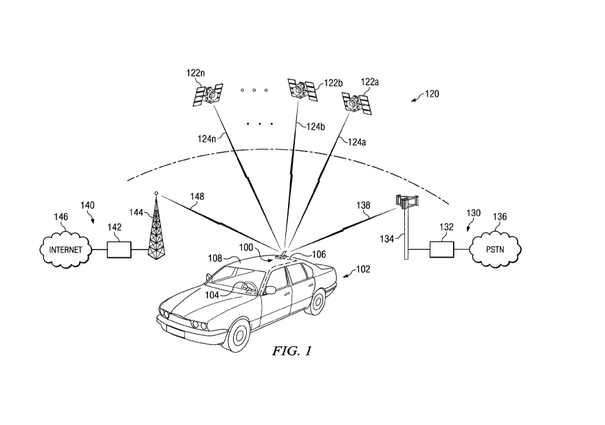
[0015] FIG. 1 is an illustration of an exemplary vehicle including a GPS, GSM,
and WLAN
antenna according to one embodiment;
[0016] FIG. 2 is an illustration of a perspective view of an exemplary GPS,
GSM, and WLAN
antenna with cover according to one embodiment;
[0017] FIG. 3A is an illustration of a perspective view of the GPS, GSM, and
WLAN antenna of
FIG. 2 without cover according to one embodiment;
[0018] FIG. 3B is an illustration of a plan view of the GPS, GSM, and WLAN
antenna of FIG 3A
according to one embodiment;
[0019] FIG. 3C is an illustration of a side view of the GPS, GSM, and WLAN
antenna of FIG. 3A
according to one embodiment;
[0020] FIG. 3D is an illustration of a front view of the GPS, GSM, and WLAN
antenna of FIG.
3A according to one embodiment;
[0021] FIG. 4A is an illustration of an exemplary circuit of a GPS, GSM, and
WLAN antenna
according to one embodiment;
[0022] FIG. 4B is an illustration of an exemplary circuit of a GPS, GSM, and
WLAN antenna
according to another embodiment;
[0023] FIG. 5 is an illustration of a plan view of a combination printed GSM
meander antenna and
printed WLAN meander antenna according to one embodiment;
[0024] FIG. 6 is an illustration of a plan view of a combination printed GSM
meander antenna and
printed WLAN meander antenna according to another embodiment;
[0025] FIG. 7A is an illustration of top view of a top patch of a dual band
GPS antenna of FIG 7B
according to one embodiment;
[0026] FIG. 7B is an illustration of a cross-section view of a dual band GPS
antenna according to
one embodiment;
[0027] FIG. 7C is an illustration of a top view of a bottom patch of the dual
band GPS antenna
according to one embodiment;
[0028] FIG. 8 is an illustration of a plan view of a GPS and satellite digital
audio radio antenna
according to one embodiment;
CA 02759193 2011-10-19
WO 2010/129628 PCT/US2010/033652
7
[0029] FIG. 9 illustrates a graph of the measurement of the combination
printed GSM meander
antenna and printed WLAN meander antenna of FIG. 5 according to one
embodiment; and
[0030] FIG. 10 is a Smith chart used for displaying an exemplary impedance
plot that shows the
impedance of combination printed GSM meander antenna and printed WLAN meander
antenna of
FIG. 5 according to one embodiment.
CA 02759193 2011-10-19
WO 2010/129628 PCT/US2010/033652
8
DETAILED DESCRIPTION OF THE DRAWINGS
[0031] The term "exemplary" is used herein to mean "serving as an example,
instance, or
illustration." Any embodiment, aspect, or design described herein as
"exemplary" is not necessarily
to be construed as preferred or advantageous over other embodiments, aspects,
or designs.
[0032] FIG. 1 is an illustration of an exemplary vehicle 102 including a GPS,
GSM, and WLAN
antenna 100 disposed on the roof 108 of vehicle 102 capable of communicating
with multiple
systems. Preferably, GPS, GSM, and WLAN antenna 100 is capable of
communicating with a GPS
120, a GSM 130, and a WLAN system 140. Additionally, GPS, GSM, and WLAN
antenna 100
includes a transceiver 104 via a conductor 106 for communicating signals
between GPS, GSM, and
WLAN antenna 100 and transceiver 104. Transceiver 104 may be incorporated
within GPS, GSM,
and WLAN antenna 100 or it may be located in a separate location of vehicle
102, such as that
shown in FIG.1
[0033] GPS 120 includes a plurality of GPS satellites 122a-122n (collectively
122) that may be in
orbit around the earth. A GPS antenna 304 (FIG. 3) has line-of-sight to one or
more GPS satellites
122 from any location on Earth unless blocked by objects (e.g., buildings,
trees, mountains, and so
on). A GPS receiver 406 (FIG. 4) may obtain a three-dimensional ("3-D")
position fix based on
measurements for at least three GPS satellites 122 or a two-dimensional ("2-
D") position fix based
on measurements for three GPS satellites 122. A position fix is an estimate of
the location of GPS
antenna 304 and/or GPS receiver 406. GPS receiver 406 may determine a time of
arrival ("TOA")
for each GPS satellite 122, which is a measure of the time it takes for GPS
signals 124a-124n
(collectively 124) to travel from GPS satellites 122 to GPS receiver 406. GPS
receiver 406 may then
calculate the distance to each GPS satellite 122 based on the TOA for GPS
satellites 122. GPS
receiver 406 may then triangulate the position of vehicle 102 on Earth based
on accurate distances
to three GPS satellites 122 and the known locations of these satellites. Since
GPS receiver 406 is
typically not synchronized with GPS satellites 122, an additional measurement
for either a fourth
GPS satellite 122 or an Earth-bound base station is used to account for
ambiguity in the timing of
GPS receiver 406.
[0034] GSM 130 may be a TDMA system that may implement one or more TDMA
standards such
as, e.g., GSM. GSM 130 may include one or more Node B 134 and a radio network
controller
("RNC") 132. Node B 134 provides over-the-air communication of GSM RF signals
for GPS,
GSM, and WLAN antenna 100 of vehicle 102 under its coverage area. RNC 132
couples to Node
Bs in GSM 130 and provides coordination and control for one or more Node B
134. In general,
Node B 134 is a fixed station that provides communication coverage for GPS,
GSM, and WLAN
CA 02759193 2011-10-19
WO 2010/129628 PCT/US2010/033652
9
antenna 100 of vehicle 102 and may also be referred to as base station(s) or
some other terminology
as would be understood by one of ordinary skill in the art. RNC 132 are
network entities that
provide coordination and control for the base stations and may also be
referred to by some other
terminology. Additionally, RNC 132 may also be in communication with a public
switched
telephone network ("PSTN") 136. Generally, GSM 130 is a cellular network and
may include a
plurality of Node B 134 and RNC 132 located in cells where vehicle 102 may
travel. Node B 134
may transmit to and receive modulated RF signals 138 from GPS, GSM, and WEAN
antenna 100
of vehicle 102.
[0035] WLAN system 140 includes one or more access points 144, such as an omni-
directional
antenna, multi-directional antenna, and/or directional antenna, for
transmitting RF signals 148 to
GPS, GSM, and WEAN antenna 100 of vehicle 102. Generally, access point 144 is
in
communication with a router 142 that is in communication with Internet 146 for
transmitting and
receiving data via RF signals 148 to GPS, GSM, and WLAN antenna 100 of vehicle
102. It should
be noted that one of ordinary skill in the art will understand that WLAN
system 140 has been
simplified to better illustrate features of GPS, GSM, and WEAN antenna 100.
Well-known
elements have not been shown, but are nonetheless part of a network embodying
features of GPS,
GSM, and WEAN antenna 100. For example, one embodiment of WEAN system 140 may
include
amplifiers, power supplies, maintenance systems, gateways, additional routers,
bridges, firewalls, and
the like.
[0036] Referring now to FIG. 2, an embodiment of GPS, GSM, and WLAN antenna
100 is shown
with a cover 202, a housing or base 204, and a GSM/WEAN antenna housing 206,
all preferably in
sealing arrangement for protecting the electronics and antennas contained
within as further
described herein from the elements and weather. Generally, cover 202, base
204, and
GSM/W]LAN antenna housing 206 have a size, form, and/or shape sufficient to
enclose the
electronics and antennas contained within them. In one embodiment, base 204
has a size and
shape sufficient to enclose GPS antenna 304 (FIG. 3) and the base portion of a
GSM/WEAN
antenna 302 (FIG. 3) as described herein. Additionally, GSM/WLAN antenna
housing 206 has a
size and shape sufficient to enclose the all or a portion of GSM/WLAN antenna
302 as described
herein. In another embodiment, cover 202, base 204, and GSM/WLAN antenna
housing 206 are a
unified single piece and not separate individual pieces. Preferably, base 204
has a lower surface that
joins in a sealing arrangement with the upper surface of roof 108 of vehicle
102. Additionally,
conductor 106 may exit the lower surface of base 204 and be disposed through
roof 108 as it is
routed to transceiver 104, in one embodiment. In another embodiment, GPS, GSM,
and WLAN
antenna 100 may be affixed or attached to other portions of vehicle 102, such
as pillars, windows,
CA 02759193 2011-10-19
WO 2010/129628 PCT/US2010/033652
trunks, bodies, etc. Cover 202, base 204, and GSM/WLAN antenna housing 206 may
be made out
of a material that is weatherproof and dustproof while allowing the GPS
antenna 304 and
GSM/WEAN antenna 302 contained within GPS, GSM, and WEAN antenna 100 to
operate
without providing unnecessary interference with RF signals.
100371 In one aspect, conductor 106 may include one or more separate
conductors, wires, or
cables, such as a radio frequency ("RF") cable 208, a RF cable 210, and a RF
cable 212. RF cable
208 is for conducting signals between GPS receiver 406 (FIG. 4) and GPS, GSM,
and WEAN
antenna 100. RF cable 210 is for conducting signals between a WLAN receiver
404 (FIG. 4) and
GPS, GSM, and WLAN antenna 100 and RF cable 212 is for conducting signals
between a GSM
receiver 402 (FIG. 4) and GPS, GSM, and WI.AN antenna 100.
100381 Referring now to FIGS. 3A-3D, an embodiment of GPS, GSM, and WEAN
antenna 100 is
shown with cover 202 and GSM/WLAN antenna housing 206 removed from base 204. A
GSM/WLAN antenna 302 and GPS antenna 304 are disposed and/or positioned within
base 204
of GPS, GSM, and WIAN antenna 100. Preferably, GSM/WLAN antenna 302 is a
substantially
planar PCB antenna having a combination GSM antenna and WEAN antenna traced on
one or
both sides of PCB antenna as further described below in FIGS. 5 and 6.
Preferably, GSM/WLAN
antenna 302 has one end that is secured to base 204 such that GSM/WLAN antenna
302 extends
in an upward position to enable incident RF signals between GSM 130 and WLAN
system 140 and
GSM/WLAN antenna 302 of GPS, GSM, and WEAN antenna 100 to be effectively
communicated. Also, GPS antenna 304 is positioned within base 204 such as in a
substantially
horizontal position such that it enables incident RF signals between GPS 120
and GPS antenna 304
of GPS, GSM, and WEAN antenna 100 to be effectively communicated.
100391 In one embodiment, roof 108 has a hole or aperture therethrough (not
shown) for receiving
a threaded member 306 of base 204 for securing GPS, GSM, and WEAN antenna 100
to vehicle
102. In one aspect, a fastener, such as a nut or threaded washer 308 may be
used with threaded
member 306 for securing GPS, GSM, and WEAN antenna 100 to roof 108 of vehicle
102. Other
types of fasteners, adhesives, and the like may be used to secure GPS, GSM,
and WEAN antenna
100 to vehicle 102, as would be commonly known to those skilled in the art.
[00401 Referring now to FIG. 4A, an embodiment of an exemplary circuit 400 is
shown that
includes conductor 106 including RF cable 208, RF cable 210, and RF cable 212
in communication
with GSM/WLAN antenna 302 and GPS antenna, respectively. RF cable 210 and RF
cable 212
may be one RF cable 408 instead of two separate RF cables. In one embodiment,
a switch 410 may
switch the signals carried in conductor 408 to RF cable 210 and RF cable 212
to WLAN receiver
404 and GSM receiver 402, respectively. GSM receiver 402, WEAN receiver 404,
and GPS receiver
CA 02759193 2011-10-19
WO 2010/129628 PCT/US2010/033652
11
406 may be part of transceiver 104 or they may be located separately or in
different locations within
vehicle 102. In another embodiment, one or more of RF cables 408, RF cable
208, switch 410, RF
cable 210, and RF cable 212 may be housed fully or partially within GPS, GSM,
and WLAN
antenna 100. In yet another embodiment, one or more of switch 410, conductor
408, RF cable 208,
RF cable 210, and RF cable 212 may be located fully or partially located
within transceiver 104.
[0041] In general, GPS, GSM, and WLAN antenna 100 may be capable of
communicating with
any number of wireless systems of different wireless technologies, such as
code division multiple
access ("CDMA"), TDMA, GSM, GPS, WLAN, and the like. In one embodiment, the
following
describes the GPS, GSM, and WLAN antenna 100 communicating with GPS 120, GSM
130, and
WLAN system 140. GPS, GSM, and WLAN antenna 100 may receive signals from one
or more
transmitting entities at any given moment, where a transmitting entity may be
a base station,
satellite, and the like; each transmitting entity may be received by each of
the GSM/WLAN antenna
302 and GPS antenna 304 of GPS, GSM, and WLAN antenna 100, albeit at different
amplitudes
and/or phases.
[0042] Referring now to FIG. 4B, another embodiment of an exemplary circuit
420 of transceiver
104 is described. As discussed above, GSM 130 and WLAN system 140 may operate
on various
frequency bands. For example, WLAN receiver 404 and GSM/WLAN antenna 302 may
operate at
2.4 GHz range and GSM receiver 402 and GSM/WLAN antenna 302 may operate at 900
MHz and
1800 MHz; 850 MHz and 1900 MHz; and/or 2100 MHz range. GPS receiver 406 and
GPS
antenna 304 may operate at 1.57542 and/or 1.2276 GHz for example. For each
frequency band,
except for the GPS frequency band, one frequency range may be used for the
downlink (i.e.,
forward link) from access point 144 and/or Node B 134 to GPS, GSM, and WLAN
antenna 100,
and another frequency range may be used for the uplink (i.e., reverse link)
from GPS, GSM, and
WLAN antenna 100 to access point 144 and Node B 134. As an example, for the
GSM850/cellular
band range (824-849 MHz) may be used for the uplink, and the 869 to 894 MHz
range may be used
for the downlink.
[0043] GPS, GSM, and WLAN antenna 100 may support one or multiple frequency
bands for each
of GPS 120, GSM 130, and WLAN system 140. In one embodiment, GPS, GSM, and
WLAN
antenna 100 communicates with one wireless system at a time, and in another
embodiment, GPS,
GSM, and WLAN antenna 100 communicates with more than one wireless system at a
time.
Various embodiments of circuit 420 of transceiver 104 of GPS, GSM, and WLAN
antenna 100 are
described.
[0044] Generally, GPS, GSM, and WLAN antenna 100 includes transceiver 104 that
may support
four frequency bands with receiving ("RX") diversity for TDMA for GSM and
support four
CA 02759193 2011-10-19
WO 2010/129628 PCT/US2010/033652
12
frequency bands with transmitting ("TX") diversity for TDMA for GSM. The quad
GSM bands
may include first, second, third, and fourth GSM transmit bands ("GTX1,"
"GTX2," "GTX3,"
"GTX4") and first, second, third, fourth GSM receive bands ("GRX1," "GRX2,"
"GRX3,"
"GRX4"). In addition, to these four frequency bands, transceiver 104 may
support a KLAN
frequency transmit band ("WTX") and a KLAN frequency receive band ("WRX").
Transceiver
104 may include a GSM/WEAN portion 422 that is in communication with GSM/WEAN
antenna
302. In addition, transceiver 104 may include a GPS portion 424 that is in
communication with
GPS antenna 304. Additionally, GSM/KLAN portion 422 of transceiver 104 may
include a switch
436 that maybe switch 410 or another switch in addition to switch 410.
GSM/WLAN portion 422
and GPS portion 424 may be in communication with a RF unit 426, which may
condition signals
for GSM/WL.AN portion 422. Switch 436 may be a transmit/receive T/R switch
that has one or
more common RF port in communication with GSM/KLAN antenna 302.
[0045] Further, switch 436 may be in communication with a duplexer 458 for the
WRX and WTX
paths. Switch 436 may further include two input RF ports for the four GSM
transmit paths,
GTX1-GTX4. Switch 436 may also include two output RF ports for the GMS receive
paths,
GRX1 and GRX2. Switch 436 couples the common RF port to one of the I/O RF
ports at any
given moment based on a control signal ("CTRL"), which may be a single-bit or
multi-bit signal.
For GSM, which may be a time division duplex ("TDD") system, uplink and
downlink
transmissions occur in different non-overlapping time intervals or time slots,
and only the transmit
path or the receive path may be active at any given moment. Switch 436
performs switching to
allow GSM/KLAN portion 422 to process either GSM or WLAN signals.
Additionally, switch 436
further performs switching between the GSM transmit and receive paths when
GSM/WEAN
portion 422 is processing GSM.
[0046] The GSM transmit path includes a power amplifier ("PA") module 442 that
receives and
amplifies a GSM transmit signal (GTX1-GTX4) from RF unit 426 and provides a
GSM uplink
signal for transmission via GSM/KLAN antenna 302. PA module 442 may have a
variable gain
that may be adjusted based on a gain control signal, which may come from a
modem processor 432.
The gain control signal may ramp-up or ramp-down the gain of PA module 442.
The amplitude of
the GSM uplink signal may also be controlled by the gain control signal and
the phase of the GSM
uplink signal may be controlled by modem processor 432 to achieve any
modulation, such as
Gaussian minimum-shift keying ("GMSK"), phase-shift keying ("PSK"), offset
quadrature phase-
shift keying ("OQPSK"), quadrature amplitude modulation ("QAM"), and the like.
The GSM
transmit and receive paths may be designed to be compliant with GSM system
requirements
described in 3GPP TS 51.010, which is publicly available, for example.
CA 02759193 2011-10-19
WO 2010/129628 PCT/US2010/033652
13
[0047] The first and third GSM receive paths, GRX1 and GRX3, may each include
a GMS filter
440 and 438, respectively, that filters a received signal from GSM/WLAN
antenna 302 and a low
noise amplifier ("LNA") 454 and 456, respectively, that amplifies the filtered
signal from filters 440
and 438 and provides GSM received signals (GRX1 and GRX3) to RF unit 426. GSM
filters 440
and 438 may be bandpass filters that are implemented with a surface acoustic
wave ("SAW") filter
having a bandwidth equal to the first or second GSM receive signals (GRX1 and
GRX3). Also,
GSM filters 440 and 438 may filter out large amplitude undesired signals (or
"jammers") and other
out-of-band signals transmitted by other wireless systems.
[0048] The WEAN transmit path includes a filter 464, a power amplifier 466,
and an isolator 470.
Filter 464 filters a WTX from RF unit 426 and provides a filtered WEAN signal.
Filter 464 may be
implemented with a SAW filter having a bandwidth equal to the WEAN transmit
band. Power
amplifier 466 amplifies the filtered WLAN signal and provides a WEAN uplink
signal. Isolator 470
couples the WLAN uplink signal to duplexer 458 and prevents the signal from
duplexer 458 from
coming back to power amplifier 466, and provides an impedance load for power
amplifier 466.
Duplexer 458 routes the WEAN uplink signal from isolator 470 to switch 436 for
transmission via
GSM/WEAN antenna 302.
[0049] Duplexer 458 also receives, via switch 436, the received signal from
GSM/WLAN antenna
302 and routes the received signal to the WEAN receive path. Duplexer 458
provides isolation
between the transmit path and the main receive path for WEAN, filters out
undesired signal
components for each of these two paths, and supports simultaneous operation of
these two signal
paths for full-duplex communication. The WRX path includes a LNA 460 and a
filter 462. LNA
460 amplifies the received signal from GSM/WEAN antenna 302 and provides an
amplified
received signal. Filter 462 filters the amplified received signal and provides
a WRX to RF unit 426.
Filter 462 may be implemented with a SAW filter having a bandwidth equal to
the WLAN receive
band, WRX. Duplexer 458 performs filtering to preselect the WRX band and
filter 462 provides
additional filtering to remove leakage of the WEAN uplink signal coming from
the WLAN transmit
path.
[0050] RF unit 426 performs signal conditioning for GSM and WEAN signals for
all of the
transmit and receive paths. For each GSM received signal and each WEAN
received signal, RF unit
426 may perform frequency down-conversion, demodulation, filtering,
amplification, and gain
control. For each GSM transmit signal and each WEAN transmit signal, RF unit
426 may perform
filtering, amplification and gain control, modulation, and frequency up-
conversion. RF unit 426
may utilize a super-heterodyne architecture or a direct-conversion
architecture. The super-
heterodyne architecture may use multiple stages, such as frequency down-
conversion from RF to an
CA 02759193 2011-10-19
WO 2010/129628 PCT/US2010/033652
14
intermediate frequency ("IF") in one stage, and (e.g., quadrature)
demodulation from IF to
baseband in another stage. The direct-conversion architecture uses a single
stage to perform
demodulation and frequency downconversion from RF directly to baseband.
Similarly, modulation
and frequency up-conversion are performed in multiple stages for the super-
heterodyne
architecture and in a single stage for the direct-conversion architecture. RF
unit 426 also performs
modulation and demodulation for each wireless system based on the modulation
scheme employed
by that system and using techniques known in the art. For example, modulation
for GSM may be
performed with an offset phase locked loop ("OPLL") or a polar modulation
scheme.
[0051] Additionally, GSM/WLAN portion 422 may include a diplexer 444 that
couples to
GSM/WLAN antenna 302, obtains the received signal from GSM/WLAN antenna 302,
provides
first and second diplexer output signals to the second and fourth GSM receive
paths (GRX2 and
GRX4), respectively. The second GSM receive path includes a filter 446 and an
LNA 450 that filter
and amplify the first diplexer output signal and provide a second GSM received
signal (GRX2) to
RF unit 426. The fourth GSM receive path (GRX4) includes a filter 448 and an
LNA 452 that filter
and amplify the second diplexer output signal and provide a fourth GSM
received signal (GRX4) to
RF unit 426. Filters 446 and 448 may be SAW filters having bandwidths equal to
the second and
fourth GSM receive bands, respectively.
[0052] A modulator/demodulator ("modem") processor 432 performs baseband modem
processing for GSM and WLAN. For each transmit path, modem processor 432
encodes,
interleaves, and modulates data to obtain data symbols, which are modulation
symbols for data.
Modem processor 432 further performs physical layer processing on the data
symbols and pilot
symbols, which are modulation symbols for a pilot, in accordance with the
wireless system. For
example, modem processor 432 may channelize (or "cover") and spectrally spread
(or "scramble")
the data and pilot symbols to obtain data chips. For each receive path, modem
processor 432
performs the complementary physical layer processing (e.g., spectral
despreading and
dechannelization) to obtain received symbols, and further demodulates,
deinterleaves, and decodes
the received symbols to obtain decoded data. The modem processing for GSM is
described in
3GPP TS 05 documents, and the modem processing for WLAN is dependent on the
WLAN
standard being implemented, such as IEEE 802.11 a/b/g/n. Modem processor 432
also performs
analog-to-digital conversion for each receive path and digital-to-analog
conversion for each transmit
path. Although not shown in FIG. 4B, modem processor 432 may also interface
with a memory
unit 428, multimedia units (e.g., a camera), I/O units (e.g., a touch screen,
a display unit, a keypad, a
speaker, and/or a microphone), and the like. Modem processor 432 may be
implemented with one
or more application specific integrated circuits ("ASICs").
CA 02759193 2011-10-19
WO 2010/129628 PCT/US2010/033652
[0053] A main oscillator 434 provides a reference oscillator signal (at a
predetermined frequency)
to RF unit 426 and modem processor 432. Main oscillator 434 may be implemented
with a voltage-
controlled temperature-compensated crystal oscillator ("VCTCXO") or some other
types of
oscillator known in the art. RF unit 426 may include built-in voltage-
controlled oscillators
("VCOs") and phase locked loops ("PLLs"). One set of VCO and PLL may be used
for each
signal path that may be "tuned" (i.e., adjusted in frequency) independently.
Each set of VCO and
PLL receives the reference oscillator signal from main oscillator 434 and
generates a local oscillator
("LO") signal at the desired frequency. A controller 430 controls the
operation of modem
processor 432 and possibly RF unit 426. Memory 428 provides storage for
controller 430 and
modem processor 432.
[0054] Additionally, transceiver 104 may include a GPS portion 424 that
supports GPS signals.
GPS portion 424 includes a filter 468 that is in communication with GPS
antenna 304 for GPS,
filters a received signal from GPS antenna 304, and provides a GPS received
signal to RF unit 426.
GPS antenna 304 may be designed for one or more GPS bands, such as 1.227 GHz
and/or 1.575
GHz, as further described below with reference to FIG. 7. Filter 468 may be
implemented with a
SAW filter having a bandwidth equal to the GPS band, for example.
[0055] Referring now to FIG. 5, an illustration of a plan view of an
embodiment of a
GSM/WEAN printed meander antenna 500 having different widths and lengths are
shown. In one
aspect, GSM/WEAN printed meander antenna 500 is printed on a PCB 508. In FIG.
5,
GSM/WEAN printed meander antenna 500 is shown with a GSM printed meander
antenna
portion 502, 506, and WEAN printed meander antenna portion 504. GSM printed
meander
antenna portion 502, 506 and WLAN printed meander antenna portion 504 may be
connected to
transceiver 104 via conductor 106. GSM printed meander antenna portion 502,
506 and WEAN
printed meander antenna portion 504 are printed on one side or both sides of
PCB 508. GSM
printed meander antenna portion 502, 506 and WEAN printed meander antenna
portion 504 may
further include an inductor (not shown) disposed between them for additional
impedance tuning of
GSM/WEAN printed meander antenna 500. In one embodiment, GSM/WLAN printed
meander
antenna 500 may further include a resistor (not shown) for providing
additional frequency
bandwidth.
[0056] In one embodiment, GSM printed meander antenna portion 502 may include
a antenna
trace line antenna trace line 502a, antenna trace line 502b, antenna trace
line 502c, antenna trace line
502d, and antenna trace line 502e (collectively 502). Antenna trace lines 502a
and 502b may have a
length L,a from about 84 millimeters ("mm") to about 28 mm. In another aspect,
antenna trace
lines 502a and 502b may have a length L,a from about 70 mm to about 42 mm.
Preferably, antenna
CA 02759193 2011-10-19
WO 2010/129628 PCT/US2010/033652
16
trace lines 502a and 502b may have a length L,a of 56 mm. Antenna trace line
502a may have a
length Lea from about 15 mm to about 5 mm. In another aspect, antenna trace
line 502a may have
a length Lea from about 13 min to about 8 mm. Preferably, antenna trace line
502a may have a
length Lea of 10 mm. Additionally, antenna trace line 502a may have a width
W3a from about 3 mm
to about 1 mm. In another aspect, antenna trace line 502a may have a width W3a
from about 3 mm
to about 2 mm. Preferably, antenna trace line 502a may have a width W3a of 2
mm.
[0057] In one aspect, antenna trace line 502b has a length L3a of from about
60 mm to about 20
mm. In another aspect, antenna trace line 502b has a length L3a of from about
50 mm to about 30
mm. Preferably, antenna trace line 502b has a length L3, of 40 mm. Antenna
trace line 502b has a
width W2a of from about 10 mm to about 3 mm. In one aspect, antenna trace line
502b has a width
W2a of from about 8 mm to about 5 mm. Preferably, antenna trace line 502b has
a width W2a of 7
mm.
[0058] In one aspect, antenna trace line 502c has a length L6a of from about
13 mm to about 4 mm.
In another aspect, antenna trace line 502c has a length L6a of from about 11
mm to about 7 mm.
Preferably, antenna trace line 502c has a length Lea of 9 mm. Antenna trace
line 502c has a width
W,a of from about 26 mm to about 9 mm. In one aspect, antenna trace line 502c
has a width W,a
of from about 21 mm to about 13 mm. Preferably, antenna trace line 502c has a
width W,,, of 17
mm. Additionally, the combined length of antenna trace line 502d and antenna
trace lines 502e has
a length Loa of from about 29 mm to about 10 mm. In another aspect, the
combined length of
antenna trace line 502d and antenna trace lines 502e has a length Loa of from
about 24 mm to about
14 mm. Preferably, antenna trace line 502d and antenna trace lines 502e has a
length Loa is 19 mm.
[0059] In one aspect, antenna trace line 502d has a length L9a of from about
12 mm to about 4
mm. In another aspect, antenna trace line 502d has a length Lea of from about
10 mm to about 6
mm. Preferably, antenna trace line 502d has a length L3a of 8 mm. Antenna
trace line 502d has a
width W4a of from about 5 mm to about 2 mm. In one aspect, antenna trace line
502d has a width
W4a of from about 4 mm to about 3 mm. Preferably, antenna trace line 502d has
a width W4a of 3
mm.
[0060] In one aspect, antenna trace line 502e has a length L5, of from about 3
mm to about 1 mm.
In another aspect, antenna trace line 502e has a length L5a of from about 3 mm
to about 2 mm.
Preferably, antenna trace line 502e has a length L3a of 2 mm. Antenna trace
line 502e has a width
W5a of from about 9 mm to about 3 mm. In one aspect, antenna trace line 502e
has a width W5a of
from about 8 mm to about 5 mm. Preferably, antenna trace line 502e has a width
W5a of 6 mm.
[0061] In one aspect, antenna trace line of WLAN printed meander antenna
portion 504 ("antenna
trace line 504") has a length L8a of from about 23 mm to about 8 mm. In
another aspect, antenna
CA 02759193 2011-10-19
WO 2010/129628 PCT/US2010/033652
17
trace line 504 has a length Laa of from about 19 mm to about 11 mm.
Preferably, antenna trace line
504 has a length L8, of 15 mm. Antenna trace line 504 has a width W6a of from
about 7 mm to
about 2 mm. In one aspect, antenna trace line 504 has a width W6a of from
about 6 mm to about 4
mm. Preferably, antenna trace line 504 has a width Woa of 5 mm.
[0062] In one aspect, GSM printed meander antenna portion 506 ("antenna trace
line 506) has a
length L7a of from about 37 mm to about 12 mm. In another aspect, antenna
trace line 506 has a
length L7a of from about 31 mm to about 19mm. Preferably, antenna trace line
506 has a length L7a
of 25 mm. Antenna trace line 506 has a width W7a of from about 8 mm to about 3
mm. In one
aspect, antenna trace line 506 has a width W7a of from about 6 mm to about 4
mm. Preferably,
antenna trace line 506 has a width W7a of 5 mm.
[0063] In one embodiment, antenna trace line 502a and antenna trace line 502b
extend laterally or
vertically from the lower end of PCB 508 to the upper end of PCB 508. In this
embodiment,
antenna trace line 502c may extend longitudinally or horizontally from one
side of antenna trace
line 502c towards the other side of PCB 508 as shown. Further, antenna trace
line 502d may
extend laterally or vertically from the upper end of PCB 508 towards the lower
end of PCB 508.
Antenna trace line 502e may extend longitudinally or horizontally from one end
of antenna trace
line 502d towards antenna trace line 502b. In one embodiment, WLAN printed
meander antenna
portion 504 extends laterally or vertically from the lower end of PCB 508
toward the upper end of
PCB 508, although it preferably terminates prior to antenna trace line 502e.
Additionally, GSM
printed meander antenna portion 506 also extends laterally or vertically from
the lower end of PCB
508 toward the upper end of PCB 508, although it also preferably terminates
prior to antenna trace
line 502e.
[0064] In the representative embodiments described herein, terms such as
"above," "below,"
"upper," "lower," etc., are used for convenience in referring to the
accompanied drawings. In
general, "above," "upper," "upward" and similar terms refer to a direction
that is commonly
thought of as vertically upward and the terms "below," "lower," and "downward"
and similar terms
refer to a direction in the opposite direction or vertically downward as
commonly known. For
purposes of this discussion, the relativity of these terms may be thought of
in the context of the use
and operation of the present GPS, GSM, and WLAN antenna 100. In one
embodiment, the term
"lower" may refer to the lower end of GPS, GSM, and WLAN antenna 100 that
affixes to roof 108
of GPS, GSM, and WLAN antenna 100. Thus, the term "upper" may refer to the
upper end of
GPS, GSM, and WLAN antenna 100 that extends away from roof 108 of GPS, GSM,
and WLAN
antenna 100.
CA 02759193 2011-10-19
WO 2010/129628 PCT/US2010/033652
18
[00651 Referring to FIG. 6, an illustration of a plan view of another
embodiment of a
GSM/WEAN printed meander antenna 600 having different widths and lengths are
shown. In one
aspect, GSM/WEAN printed meander antenna 600 is printed on a PCB 606. In FIG.
6,
GSM/WLAN printed meander antenna 600 is shown with a printed meander antenna
portion 602
and printed meander antenna portions 604a, 604b. Printed meander antenna
portion 602 and
printed meander antenna portions 604a, 604b may be connected to transceiver
104 via conductor
106. Printed meander antenna portion 602 and printed meander antenna portion
604a, 604b are
printed on one side or both sides of PCB 606. Printed meander antenna portion
602 and printed
meander antenna portion 604a, 604b may further include an inductor (not shown)
disposed
between them for additional impedance tuning of GSM/WLAN printed meander
antenna 600. In
one embodiment, GSM/WEAN printed meander antenna 600 may further include a
resistor (not
shown) for providing additional frequency bandwidth.
[00661 In one embodiment, GSM printed meander antenna portion 602 may each
include 20
longitudinal or horizontal antenna trace lines of GSM printed meander antenna
portion 602, 602a-
602t (collectively 602). In one embodiment, antenna trace lines 602 may have a
length Llb from
about 104 mm to about 35 mm. In another aspect, antenna trace lines 602 may
have a length Lib
from about 86 mm to about 52 mm. Preferably, antenna trace lines 602 may have
a length Lib from
about 86 mm is 69 mm. The length Llb includes all the bends of the antenna
trace lines 602. In
one aspect, printed meander antenna portion 602 and printed meander antenna
portions 604a, 604b
may have a width W,b from about 39 mm to about 13 mm. In another aspect,
printed meander
antenna portion 602 and printed meander antenna portions 604a, 604b may have a
width W,b from
about 32 mm to about 20 mm. Preferably, printed meander antenna portion 602
and printed
meander antenna portions 604a, 604b may have a width W,b of 26 mm.
[00671 In one aspect, antenna trace lines 604a and 604b may have a length Lb
from about 54 mm
to about 18 mm. In another aspect, antenna trace lines 604a and 604b may have
a length L2b from
about 45 mm to about 27 mm. Preferably, antenna trace lines 604a and 604b have
a length L2b of
36 mm. Antenna trace lines 604a and 604b may have a width W2b from about 8 mm
to about 3
mm. Antenna trace lines 604a and 604b have a width W2b from about 6 mm to
about 4 mm.
Preferably, antenna trace lines 604a and 604b have a length L2b is 5 mm.
[00681 The individual antenna trace lines 602a-602t may have a length L3b from
about 3 mm to
about 1 mm. Further, individual antenna trace lines 602a-602t may have a
length L3b from about 2
mm to about 1 mm. Preferably, individual antenna trace lines 602a-602t may
have a length L3b of 2
mm. It may be common to consider L3b as a width of the entire printed meander
antenna portion
602 in one embodiment although its dimensions are being provided as a length.
As can be seen
CA 02759193 2011-10-19
WO 2010/129628 PCT/US2010/033652
19
from FIG. 6, the widths of the individual antenna trace lines 602a-602t may
vary. For example, the
upper portion of printed meander antenna portion 602 is shown having a
slightly wider width of
individual antenna trace lines 602a-602t than the lower portion of printed
meander antenna portion
602. In one aspect, the width W3b of individual antenna trace lines 602a-602t
may be from 23 mm
to about 8 mm. In another aspect, the width W3b of individual antenna trace
lines 602a-602t may
from about 19 mm to about 12 mm. Preferably, the width W3b of individual
antenna trace lines
602a-602t is 15 mm. Further, the width W4b of individual antenna trace lines
602a-602t may be
from 30 mm to about 10 mm. Also, the width W4b of individual antenna trace
lines 602a-602t may
be from 25 mm to about 15 mm. Preferably, the width W4b of individual antenna
trace lines 602a-
602t is 20 mm. As shown, the upper portion of printed meander antenna portion
602 may have the
width W4b and the lower portion of printed meander antenna portion 602 may
have the width of
W3b.
[0069] In one embodiment, antenna trace lines 602a-602t may extend
longitudinally or horizontally
from the lower end of PCB 606 and meander back and forth substantially
adjacent to each other as
the entire length of printed meander antenna portion 602 extends towards the
upper end of PCB
606. The printed meander antenna portions 604a, 604b may extend vertically or
laterally from the
lower end of PCB 606 towards the upper end of PCB 606 and may end at a point
where the widths
of 602a-602t increase in width. In one aspect, any or all of the trace lines
described herein may be
made from a conducting material, such as copper.
[0070] In one embodiment, symmetrical printed meander dipole antennas 600 and
700 may further
include a ground spot that may be located on the bottom side of PCB 508 and
606, respectively,
that may be used as a ground for the amplifier circuit when using GSM/WLAN
printed meander
antennas 500 and 600 in an active receiving embodiment. In one aspect, the
lengths and number of
bends of antenna trace lines 602a-602t may be chosen using electromagnetic
software, such as
IE3D, to provide a desirable resistance, such as 50 Ohms input impedance for a
particular
application. Additionally, impedance tuning may further be optimized by using
inductors in
addition to the additional cutting of the trace lines as described herein.
[0071] PCBs 508 and 606 may be a width that is desirable for a particular
application. The width
of the printed antenna trace lines may be any desired width for a particular
application. PCBs 508
and 606 may further include a ground plane (not shown) with a dielectric board
(not shown)
disposed thereon. In one embodiment, the dielectric board of PCBs 508 and 606
may be
composed of FR-4 material and have a thickness of approximately 1.6 mm and a
relative
permittivity of 4.4. It should be understood in the art that the configuration
of the outputs of
PCBs 508 and 606 may have alternative configurations and the dielectric board
may be composed
CA 02759193 2011-10-19
WO 2010/129628 PCT/US2010/033652
of another material and have a different thickness and provide an operable
antenna solution. In
one embodiment, ground pads are used as the second "arm" on each of these
GSM/WLAN
printed meander antenna 500 and GSM/WLAN printed meander antenna 600; the pads
serve
concomitantly as LNA grounds. The LNA located at the antenna trace line side
may increase the
sensitivity of a particular receiver as described herein, for example.
10072] As further understood in the art, physical parameters of GSM/WEAN
printed meander
antennas 500 and 600 may be used for adjusting bandwidth to receive signals,
such as RF signals,
over a frequency band for tuning impedance of the antenna over the frequency
band, and for
adjusting gain over the bandwidth. If the output of the GSM/WLAN printed
meander antennas
500 and 600 has a certain impedance that includes only resistive component
(reactive component
value is equal to), then if the RF circuit has the same input impedance, a
voltage standing wave ratio
("VSWR") will have a value of 1.0 and the RF signal will be completely input
into the RF circuit
(i.e., no part of the RF signal will reflect back from the RF circuit). If the
output impedance of
GSM/WEAN printed meander antennas 500 and 600 and the input impedance of the
RF circuit do
not match, the VSWR increases to a multiple of 1.0, where the higher the
ratio, the higher the
VSWR and the lower the input of the RF input impedance of the RF circuit. In
one embodiment,
these fundamental RF principles may drive the configuration of GSM/WEAN
printed meander
antennas 500 and 600. Because slight differences in the configuration of
GSM/WEAN printed
meander antennas 500 and 600 can have large effects in tuning over the
frequency range of a
desired application(s), many configurations of the basic structure of GSM/WEAN
printed meander
antennas 500 and 600 may be used to provide RF output to any of the receivers
described herein at
a certain resistance (e.g., 50 Ohms) to match a resistance of an RF circuit
(e.g., 50 Ohms).
100731 In one embodiment, GPS antenna 304 is a single feed antenna that
operates at 1.227 GHz
frequency, and in another embodiment, GPS antenna 304 is a single feed antenna
that operates at
1.575 GHz frequency. In another embodiment, GPS antenna 304 may be single feed
dual band
GPS antenna, which operates at both 1.227 GHz and 1.575 GHz frequencies. In
both of these
embodiments, GPS antenna 304 may be a single patch antenna or double patch
antenna, for
example.
100741 Referring now to FIGS. 7A-7C, an embodiment of a single feed dual band
GPS antenna
700 is shown. Dual band GPS antenna 700 includes a top patch antenna 702 and a
bottom patch
antenna 704. Dual band GPS antenna 700 is a single feed low-profile circularly
polaraized ("CP")
microstrip antenna. Dual band GPS antenna 700 may be in place of GPS antenna
304 or in
addition to GPS antenna 304 in GPS, GSM, and WLAN antenna 100. Dual band GPS
antenna 700
operates in both the 1.227 GHz and 1.575 GHz frequencies. Top patch antenna
702 is
CA 02759193 2011-10-19
WO 2010/129628 PCT/US2010/033652
21
substantially a square patch that is printed on FR4 substrate of thickness of
1.6 mm with a relative
permittivity of 4.4. Top patch antenna 702 further includes a contact feed or
probe feed 712 that
excites top patch antenna 702 through a via 708 located in bottom patch
antenna 704. Additionally,
bottom patch antenna 704 may have a ground plane 710 disposed on the lower
side of bottom
patch antenna 704. In one aspect, ground plane 710 may have dimension of 100
mm by 100 mm.
Probe feed 712 may be connected to RF cable 208 for providing signals to GPS
receiver 406.
[0075] Located between top patch antenna 702 and bottom patch antenna 704 is a
thin air layer
706. By varying the thickness of air layer 706, the frequency ratio of top
patch antenna 702 and
bottom patch antenna 704 can be varied. In one aspect, the resonant lengths L,
and Lei of top
patch antenna 702 and bottom patch antenna 704, respectively, may about the
same, but not quite
equal. They generally will depend on the lower CP frequency at 1.227 GHz. In
one embodiment,
to excite top patch antenna 702 at 1.227 GHz, it is preferred that the
resonant L, be slightly larger
than L2. In one embodiment, L, is approximately 60 mm and is a square with
opposing corners
with a truncated side length LC, of 8.5 mm. Then another CP operation at the
desired frequency of
1.575 GHz, bottom patch antenna 704 preferably has a resonant L2 of
approximately 59 mm and is
square with opposing corners with a truncated side length LC2 of 7.5 mm. Air
layer 706 is
preferably 0.45 mm. For bottom patch antenna 704, the obtained impedance
bandwidth,
determined from 10-db return loss, is 53 MHz, or about 4.3% with respect to
1.227 GHz. For top
patch antenna 702, impedance bandwidth is 44 MHz, or about 2.8% referenced to
1.575 GHz.
[0076] Referring to FIG. 8, an embodiment of a combination GPS and satellite
digital audio radio
antenna ("GPS SDAR antenna") 800. As noted above with respect to dual band GPS
antenna 700,
GPS SDAR antenna 800 may be used in place of GPS antenna 304 or in addition to
GPS antenna
304. GPS signals 124 are right hand circular polarization ("RHCP") signals and
SDARS are left
hand circular polarization ("LHCP") signals, they may be operated at the same
time without
interfering with each other's passive performance. GPS SDAR antenna 800 may
include a first top
metallization element 802 and a second top metallization element 804 disposed
over top surface of
a dielectric material 14. First top metallization element 802 includes
opposing cut corners 806, 808,
which results in a LHCP polarized antenna element, and second top
metallization element 804
includes straight-edge interior corners 810, 812 (i.e. non-perpendicular
corners), which results in a
RHCP polarized antenna element. A feed pin 814 is in direct contact with first
top metallization
element 802 and extends perpendicularly through the dielectric material 816
through an opening
818 formed in a substantially rectangular bottom metallization element (not
shown). As illustrated,
dielectric material 816 isolates the feed pin 814 from contacting the bottom
metallization element.
CA 02759193 2011-10-19
WO 2010/129628 PCT/US2010/033652
22
[0077] Second top metallization 804 element is shaped as a substantially
rectangular ring of
material that encompasses a substantially rectangular sheet of material that
defines first top
metallization element 802. Each first and second top metallization elements
802, 804 may be
separated by a ring 820 of dielectric material that may be integral with the
dielectric material 816,
which supports first and second top metallization elements 802, 804. Although
first and second
top metallization elements 802, 804 include a thickness, T, and are shown
disposed in the top
surface of dielectric material 816, first and second metallization elements
802, 804 may be placed
over a top surface of dielectric material 816 and, as such, a separate ring
822 of dielectric material
may be placed over the top surface of the dielectric material 816. In one
aspect, an outer ring of
dielectric material 822 may be placed over top surface to encompass an outer
periphery of the
second top metallization element 804. Additional disclosure relating to one
embodiment of GPS
SDAR antenna 800 are described in U.S Pat. No. 7,253,770 issued August 7, 2007
to Yegin et al;
U.S. Pat. No. 7,405,700 issued July 29, 2008 to Duzdar et al.; and U.S. Pat.
No. 7,164,385 issued
January 16, 2007 to Duzdar et al.; which are all incorporated herein by
reference in their entirety.
GPS SDAR antenna 800 may be connected to GPS antenna 304 and satellite digital
audio radio
receiver (not shown) via RF cable 208 or other conductor means as commonly
know to those
skilled in the art.
[0078] Referring to FIG. 9, a graph 900 shows a GSM/WEAN printed meander
antenna 500 with
resistance equal to 0 Ohms. As can be seen from graph 900, the measurement of
the frequency
bandwidth is approximately 1638.77 MHz, beginning at 824.0000 MHz and ending
at 2462.7667
MHz. Referring to FIG. 10, a Smith chart 1000 is shown that is used for
displaying an exemplary
impedance plot 1020 for GSM/WLAN printed meander antenna 500. In designing a
RF signal
path, for example, a network analyzer that is capable of generating the Smith
chart 1000 may be
used to analyze impedances over a frequency range for operating GSM/WLAN
printed meander
antenna 500. As shown on the Smith chart 1000, the input impedance plot 1020
shows input
impedances of GSM/WEAN printed meander antenna 500 having an impedance of 50
Ohms.
Because GSM/WLAN printed meander antenna 500 and circuits 400 and 420 maybe
mismatched
in impedance, a VSWR value is greater than 1 results. A Smith chart has a
normalized impedance
plane 1002 defining an inductive impedance (positive imaginary parts) 1006
above the normalized
impedance plane 1002 and a capacitive impedances (negative imaginary parts)
1004 below the
normalized impedance plane 1002. In Smith chart 1000, a marker 1008 shows an
impedance or
resistance of 22.96 Ohms at 824.000 MHz; a marker 1010 shows an impedance of
91.45 Ohms at
960.000 MHz; a marker 1012 shows an impedance of 35.78 Ohms at 1710.000 MHz; a
marker 1014
shows an impedance of 34.73 Ohms at 2039.967 MHz; a marker 1016 shows an
impedance of
CA 02759193 2011-10-19
WO 2010/129628 PCT/US2010/033652
23
24.90 Ohms at 2380.767 MHz; and a marker 1018 shows an impedance of 34.93 Ohms
at 2462.767
MHz.
100791 The previous detailed description is of a small number of embodiments
for implementing
the GPS, GSM, WLAN antenna and is not intended to be limiting in scope. One of
skill in this art
will immediately envisage the methods and variations used to implement this
invention in other
areas than those described in detail. The following claims set forth a number
of the embodiments
of the GPS, GSM, WLAN antenna disclosed with greater particularity.