Note: Descriptions are shown in the official language in which they were submitted.
CA 02759472 2011-10-20
WO 2010/126682 PCT/US2010/030106
APPARATUS AND METHOD FOR MEASURING MATERIAL THICKNESS
BACKGROUND OF THE INVENTION
This invention relates generally to ultrasonic probes, and more particularly
to dual
phased array ultrasonic probes that measure the thickness of materials.
Ultrasonic testing is a type of non-destructive testing that is used to
inspect test object
in order to identify and/or characterize defects, flaws, and other anomalies
in the test
object. Testing equipment that is used in ultrasonic testing generally
includes a probe
that sends and receives signals, a test instrument that operates the probe,
and a cable
that transmits information between the probe and the test instrument.
The probe incorporates transducer elements that are constructed of
piezoelectric
materials that are responsive to certain stimuli in a manner conducive to non-
destructive testing. For example, certain transducer elements that are found
in the
probes generate acoustic waves in response to electrical waveform pulses that
are
applied to electrodes connected to the element. These elements are also
responsive to
acoustic waves, such as those acoustic waves that are reflected from the test
object.
This generates a voltage difference across electrodes that are connected to
the
element. For purposes of ultrasonic testing, transducer elements are used to
transmit
acoustic waves into the test object, transducer elements are used to capture
the
reflection of those acoustic waves, and the resultant voltage differences
caused by the
reflected waves are processed in order to analyze the test object.
While many probes utilize the same transducer elements to transmit and to
receive the
acoustic waves, such probes are typically not suited to measure the thickness
of
materials that are corroded because of the noise, e.g., the backscattered
noise, which is
generated by the corrosion. Instead, probes that are used to measure the
thickness of
corroded materials typically have a pair of transducer elements, one that
transmits the
acoustic wave to the test object, and one that receives the reflected acoustic
waves
from the test object. Probes that are of the type suited to measure the
thickness of
corroded materials, however, are not often compatible with test objects that
have large
surface areas.
1
CA 02759472 2011-10-20
WO 2010/126682 PCT/US2010/030106
One reason for this is because the field of view of these probes is much
smaller than
the area of interest of the test object. This makes testing large areas of
interest highly
inefficient, and in many cases very costly. Moreover, because the ratio of the
field of
view of the probe to the area of interest of the test object is small, the
likelihood
increases that defects in the area of interest will be missed because the
defects may
not fall within the field of view of the probe.
Therefore, it would be advantageous to have an apparatus that can provide
highly
accurate measurement of material thickness for large areas of interest. It
would also
be advantageous to have an apparatus that can measure the thickness of
corroded
materials, while being configured in a manner so as to improve the inspection
of test
objects by reducing both the inspection costs, and the likelihood that defects
are
missed during the inspection.
BRIEF DESCRIPTION OF THE INVENTION
In one embodiment, a measurement probe for measuring a thickness of a test
object,
the measurement probe comprising a delay block including a body having a
longitudinal axis, the body including a scan surface to be placed proximate
the test
object, and a support surface opposite the scan surface. The measurement probe
also
comprising a plurality of transducer elements acoustically coupled to the
support
surface in a manner forming an active group, the active group including a
transmitter
side for generating an ultrasound beam, and a receiver side for receiving an
echo
signal, the receiver side in a spaced relationship with the transmitter side,
the spaced
relationship forming a gap extending along the longitudinal axis. The
measurement
probe further comprising and a cross-talk barrier disposed in the gap in a
manner
acoustically separating the transmitter side from and the receiver side of the
active
group, wherein the receiver side includes at least one transducer element
responsive to
the echo signal that corresponds to the ultrasound beam that is directed into
the test
object from at least one transducer element on the transmitter side.
In another embodiment, a measurement system for measuring a thickness of a
material, the system comprising a measurement probe including a delay block
having
2
CA 02759472 2011-10-20
WO 2010/126682 PCT/US2010/030106
a longitudinal axis and a plurality of transducer elements acoustically
coupled to the
delay block in a manner forming an active group, the active group including a
transmitter side for generating an ultrasound beam, and a receiver side for
receiving
an echo signal, the receiver side in a spaced relationship with the
transmitter side, the
spaced relationship forming a gap about the longitudinal axis, the gap
including a
cross-talk barrier disposed in a manner acoustically separating the
transmitter side and
the receiver side. The system also comprising a test instrument coupled to the
measurement probe, the test instrument including an interface controlling at
least one
transducer element in the active group in a manner causing a first parameter
of the
ultrasound beam, wherein the receiver side includes at least one transducer
element
responsive to the echo that corresponds to the ultrasound beam.
In still another embodiment, a method of imaging a test object with a
measurement
probe having a delay block including a body having a longitudinal axis, the
body
including a scan surface to be placed proximate the test object, and a support
surface
opposite the scan surface. The method comprises forming a plurality of active
groups
on the support surface with a plurality of transducer elements, each of the
active
groups including a transmitter side for generating an ultrasound beam, and a
receiver
side for receiving an echo signal, the receiver side in a spaced relationship
with the
transmitter side, the spaced relationship forming a gap extending along the
longitudinal axis. The method also comprises activating a first active group
in a
manner generating a first ultrasound beam from a first transducer on the
transmitter
side of the first active group. The method further comprises receiving the
echo signal
from the first ultrasound beam with at least one transducer element on the
receiver
side of the first active group.
BRIEF DESCRIPTION OF THE DRAWINGS
So that the manner in which the above recited features of the present
invention can be
understood in detail, a more particular description of the invention briefly
summarized
above, may be had by reference to the embodiments, some of which are
illustrated in
the accompanying drawings. It is to be noted, however, that the appended
drawings
illustrate only typical embodiments of this invention and are therefore not to
be
3
CA 02759472 2011-10-20
WO 2010/126682 PCT/US2010/030106
considered limiting of its scope, for the invention may admit to other equally
effective
embodiments. The drawings are not necessarily to scale, emphasis generally
being
placed upon illustrating the principles of certain embodiments of invention.
Thus, for
further understanding of the nature and objects of the invention, references
can be
made to the following detailed description, read in connection with the
drawings in
which:
FIG. 1 is a perspective view of a measurement system that includes one
embodiment
of a measurement probe.
FIG. 2 is a perspective detail view of the measurement probe of FIG. 1.
FIG. 3 is a perspective view of another embodiment of a measurement probe.
FIG. 4 is a side cross-section view of the measurement probe of FIG. 3.
FIG. 5 is a perspective view of still another embodiment of a measurement
probe.
FIG. 6 is a side cross-section view of the measurement probe of FIG. 5.
FIG. 7 is a flow diagram of a method of implementing a measurement system that
includes a measurement probe, such as the measurement probes in FIGS. 1-6.
DETAILED DESCRIPTION OF THE INVENTION
Referring now to the drawings, FIGS. 1-2 illustrate an example of a
measurement
probe 100 in one embodiment of the present invention. The measurement probe
100
can be implemented as part of a measurement system 102, where the measurement
probe 100 can be placed on a scan surface 104 of a test object 108. Exemplary
objects that can be interrogated by the measurement system 102 as the test
object 108
include, but are not limited to, pipes, ducts, plates, vessels, and tanks,
among many
others. These test objects 108 may be susceptible to corrosion such as, for
example, if
the test object 108 is exposed to materials that cause oxidation of an
opposing surface
106 that is opposite of the scan surface 104 of the test object 108. As
discussed in
more detail below, the measurement system 102 may also include a test
instrument
4
CA 02759472 2011-10-20
WO 2010/126682 PCT/US2010/030106
110 and a cable 112 that exchanges information, e.g., data, control
instructions, etc.,
between the test instrument 110 and the measurement probe 100.
The probes of the type that can be used as measurement probe 100 can have a
scan
area 114 that has a length L. The length L can vary in a manner that permits
the
measurement probe 100 to measure a variety of characteristics of the test
object 108.
These characteristics may include, but are not limited to, the material
thickness
between the scan surface 104 and the opposing surface 106 of the test object
108, the
material thickness between the scan surface 104 and the opposing surface 106
of the
test object 108 when the opposing surface 106 is corroded, as well as other
defects,
anomalies, and deviations that may be located at different depths between the
scan
surface 104 and the opposing surface 106 of the test object 108.
This is beneficial because probes like the measurement probe 100 can be used
to
interrogate the test object 108 in a manner that would normally require
separate
devices. This includes, for example, devices that have qualities that are
optimized for
detecting defects that are near the scan surface 104 of the test object 108
(hereinafter,
"near-distance detectability"), and devices that have qualities that are
optimized for
detecting defects that are located deeper in the test object 108 (hereinafter,
"far-
distance detectability"). It is likewise beneficial that the length L of the
scan area 114
can be configured so as to substantially reduce both the time that is required
to
interrogate the test object 108, as well as the likelihood that defects are
missed during
interrogation of the test object 108. Additional details about the
construction of
probes that are suited for use as the measurement probe 100 are provided in
connection with the embodiment of a measurement probe that is illustrated in
FIGS.
3-6 below. Before continuing with that description, however, a general
discussion of
the components and other aspects of the measurement probe 100 and its
implementation in the measurement system 102 follows immediately below.
In the present example, the scan area 114 of the measurement probe 100 may
include
a plurality of transducer elements 116 that can be arranged in an array 118.
The array
118 can have a transmitter side 120 and a receiver side 122, which can be
positioned
in a spaced relationship 124 from the transmitter side 120. Here, the spaced
CA 02759472 2011-10-20
WO 2010/126682 PCT/US2010/030106
relationship 124 forms a gap 126 that describes the minimum distance between
the
interior portions of the transmitter side 120 and the receiver side 122. This
distance
can vary. In one example, this distance can be less than about 0.5 mm, and in
certain
embodiments of the measurement probe 100 this distance can be from about 0 mm
to
about 0.75 mm. As discussed in more detail in connection with FIGS. 3-4 below,
embodiments of the measurement probe 100 may also include a cross-talk barrier
128,
which can be disposed in the gap 126 so as to separate the transmitter side
120 and the
receiver side 122.
The transmitter side 120 may include a plurality of transmitter elements 130
that have
a transmitter centerline 132, and the receiver side 122 may include a
plurality of
receiver elements 134 that have a receiver centerline 136. Typically the
transmitter
elements 130 and the receive elements 134 are spaced at a pitch 138, which in
the
present example is measured between the transmitter centerline 132 of adjacent
transmitter elements 130, and between the receiver centerlines 136 of adjacent
receiver elements 134. In one example, the pitch 138 can vary in a manner
consistent
with the other dimensions of the embodiments of the measurement probe 100.
The receiver elements 134 can be configured to receive echo signals from the
test
object 108. Exemplary echo signals include, but are not limited to, acoustic
signals,
and/or acoustic waves that correspond to the acoustic signals transmitted by
the
transmitter elements 130, and which are reflected back from the test object
108
toward the measurement probe 100. Each of the transmitter elements 130 and the
receiver elements 134 can be constructed, in whole or in part, of a
piezoelectric
material, including, for example, piezoelectric ceramics, lead zirconate
titanate, lead
mataniobate, piezoelectric crystals, and any combinations thereof. In one
example,
one or more of the transmitter elements 130 and one or more of the receiver
elements
134 may include a 1-3 type piezocomposite material.
In one embodiment of the measurement probe 100, the scan area 114 can have one
or
more active groups 140. Typically the active groups 140 comprise a plurality
of
transducer elements 116, and more particularly the active groups 140 may
include one
or more of the transmitter elements 130 and one or more of the receiver
elements 134.
6
CA 02759472 2011-10-20
WO 2010/126682 PCT/US2010/030106
By way of non-limiting example, each of the active groups 140 may have one of
the
transmitter elements 130 and one of the receiver elements 134, where the
receiver
element 134 receives the echo signals that correspond to the acoustic signals
that
originate from the transmitter element 130 in the active group 140. In other
examples
of the measurement probe 100, each of the active groups 140 may include any
number
of the transmitter elements 130 and the receiver elements 134.
The number of the transmitter elements 130 and the receiver elements 134 in
the
active groups 140 can be determined in accordance with the depth of the defect
in the
test object 108. Typically the depth is measured from the scan surface 104
into the
test object 108. For example, the depth of defects that require the near-
distance
detectability may be generally less than about 5 mm. On the other hand, the
depth of
defects that require the far-distance detestability may be generally greater
than, or
equal to about 5 mm, with certain embodiments of the measurement probe 100
being
configured to detect defects that are at depths of at least about 50 mm.
It is noted that the designation of "the near-distance detectability" and "the
far-
distance detectability" as used herein is merely used to designate the
relative qualities
of one embodiment of the measurement probe, e.g., the measurement probe 100.
This, however, is not meant to limit the scope or spirit of the present
disclosure,
inasmuch as embodiments of other probes disclosed, described, and contemplated
herein may have other qualities. These other qualities may be the same,
different, or
of slightly different variations so as to cause such qualities to be used for
defects that
may have depths that fall outside of the depths discussed above.
The active groups 140 that are used for the near-distance detectability may
require a
number of the transmitter elements 130 and a number of the receiver elements
134
that is less then the numbers that are required for the far-distance
detectability. In one
example, when the qualities of the measurement probe 100 are configured for
the
near-distance detectability, the active groups 140 may only have one of the
transmitter
elements 130 and one of the receiver elements 134. In another example, when
the
qualities of the measurement probe 100 are configured for the far-distance
7
CA 02759472 2011-10-20
WO 2010/126682 PCT/US2010/030106
delectability, the active groups 140 may have at least seven of the
transmitter
elements 130 and at least seven of the receiver elements 134.
Discussing the test instrument 110 in more detail, the test instrument 110
that can be
used in the present embodiment of the measurement probe 100 of FIGS. 1-2 can
be
configured to operate the measurement probe 100 so as to activate, and collect
data
from, the scan area 114. This includes, for example, being configured to
activate
particular ones of the active groups 140 of the scan area 114, and being
configured to
activate particular ones of the transmitter elements 130 and the receiver
elements 134.
Exemplary devices that are suited for use as the test instrument 110 can
include, but
are not limited to, computers (e.g., desktop computers, laptop computers,
etc.),
ultrasound instruments, ultrasound systems, and the like. An example of an
ultrasound instrument is the Phasor XS Phased Array Ultrasound Instrument
available
from GE Inspection Technologies of Lewiston, PA.
By way of non-limiting example, and as it is illustrated in FIGS. 1-2, the
test
instrument 110 can include an interface 142 that has a display 143 that
displays
information, e.g., data information, images, etc., which can be collected by
the
measurement probe 100. The interface 142 can also include one or more controls
144
that control the operation of the measurement probe 100. In one embodiment of
the
measurement probe 100, the controls 144 can be configured to select the length
L of
the scan area 114, the number of active groups 140 in the scan area 114,
and/or the
number of the transmitter elements 130 and the receiver elements 134 in each
of the
active groups 140.
In view of the foregoing, and discussing one implementation of the measurement
probe 100 and the measurement system 102 in more detail, a user, e.g., a field
engineer, can position the measurement probe 100 on the scan surface 104 of
the test
object 108 so that the acoustic signals from the transmitter elements 130 can
enter the
test object 108. The field engineer can move the probe 100 along the scan
surface
104, e.g., in a direction 146 that may be substantially perpendicular to the
scan area
114. This may cause the scan area 114 to come into contact with the area of
interest
of the test object 108. The term "area of interest" is used herein to describe
the
8
CA 02759472 2011-10-20
WO 2010/126682 PCT/US2010/030106
portion of the test object 108 where data is to be collected with the
measurement
system 102. An area of interest, for example, may include the test object 108
in its
entirety, and/or a portion of the test object 108. The area of interest may
also include
portions of the test object 108 that are corroded, and/or portions of the test
object
where defects are found. The area of interest may further include the scan
surface 104
of the test object 108 in its entirety, and/or a portion of the scan surface
104 of the test
object 108.
In one embodiment of the measurement probe 100, the field engineer can adjust
the
controls 144 of the test instrument 110 so as to accommodate changes in the
physical
characteristics of the area of interest of the test object 108. This includes
changes in
the thickness of the material between the scan surface 104 and the opposing
surface
106 of the test object 108. For example, certain portions of the test object
108 may be
corroded so that the material thickness of one portion of the test object 108
is different
than the material thickness of another portion of the test object 108. The
physical
characteristics also include the depth of the defect from the scan surface
104. For
example, one defect may have a depth within the test object 108 that is
different from
other defects within the test object 108, which are also detected with the
measurement
system 102.
To accommodate for the difference in the physical characteristics of the area
of
interest, the field engineer can adjust the controls 144 to modify one or more
parameters of the ultrasound beam that is generated by the measurement probe
100.
For example, the ultrasound beam may have a near-field parameter for near-
field
detestability and a far-field parameter for far-field detestability. These may
be
different based on the number of the transmitter elements 130 and the number
of the
receiver elements 134 that are utilized in the active groups 140. In another
example,
the near-field parameter may be different from the far-field parameter based
on the
number of active groups 140 that are found in the scan area 114. In still
another
example, each of the near-field parameter and the far-field parameter can
correspond
to different depths inside of the test object 108.
9
CA 02759472 2011-10-20
WO 2010/126682 PCT/US2010/030106
Referring next to FIGS. 3-4, and also to FIGS. 1-2, another example of a
measurement probe 200 is illustrated, where portions of the measurement
system, e.g.,
system 102 (FIG. 1), have been removed for clarity. It is noted that, where
applicable,
numerals are used to designate like components, such as those components in
FIGS.
1-2 above, but that the numerals are increased by 100. For example, the
measurement
probe 200 of FIGS. 3-4 can include a scan area 214, transducer elements 216
that can
be arranged in an array 218, and more particularly, in a transmitter side 220
and a
receiver side 222 that can be separated by a cross-talk barrier 228. In the
present
example, each of the transmitter side 220 and the receiver side 222 can
include,
respectively, a plurality of transmitter elements 230 and a plurality of
receiver
elements 234.
The measurement probe 200 can also include a wiring harness 248, and a delay
block
250. The delay block 250 can have a body 252 that has a longitudinal axis 253,
a
lower portion 254 that has a scan surface 256, and an upper portion 258 that
has a pair
of recessed areas 260. The recessed areas 260 can include a transmitter
recessed area
262 that has a transmitter support surface 264, and a receiver recessed area
266 that
has a receiver support surface 268. Embodiments of the measurement probe 200
may
also include a housing 270 that has an interior cavity 272 with a bottom
opening 274
that may be sized and configured to receive the body 252 so that at least the
upper
portion 258 of the delay block 250, the wiring harness 248, as well as the
transducer
elements 216 are surrounded by the housing 270.
A connective element 276 can also be provided and disposed, e.g., on one or
more of
the body 252 and the housing 270. Connective elements of the type used as the
connective element 276 may typically include devices for coupling the cable
112
(FIG. 1) to the measurement probe 200. This may include, for example, screw-
threaded fittings, snap fittings, pressure release fittings, deformable
fittings, quick-
release fittings, and any combinations thereof. In one example, the connective
element 276 can be adapted to mate with threaded connectors that are on the
cable
112 (FIG. 1).
CA 02759472 2011-10-20
WO 2010/126682 PCT/US2010/030106
By way of non-limiting example, the body 252 of the delay block 250 can
acoustically couple, via the scan surface 256, the transducer elements 216 to
the
surface 104 (FIG. 1) of the test object 108 (FIG. 1). The body 252 can be
constructed
monolithically, or in a number of parts that are assembled together to form
the delay
block 250. For example, the lower portion 254 that includes the scan surface
256 may
be detachable from the body 252 so that the scan surface 256 can be removed
and/or
replaced on the body 252. For example, it is contemplated that the scan
surface 256
can be removed and replaced, either in whole or in part, when the scan surface
256 is
worn, damaged, or otherwise modified in a manner that limits the capabilities
of the
measurement probe 100.
Materials that are used for the body 252 are generally selected based on their
acoustic
velocity, or the velocity of the particles in the material as the material
transmits an
acoustic wave. Typically the acoustic velocity of the materials in the body
252 can be
different from the acoustic velocity of the materials of the test object 108
(FIG. 1).
Exemplary materials include, but are not limited to, metals and plastics, and
in one
embodiment of the measurement probe 200 the materials may include one or more
of
plexi-glass and/or poly-styrene.
As it is seen in the example of FIG. 3, and more particularly in the section
view of
FIG. 4 where the measurement probe 200 is shown in one example of its
assembled
form, the recessed areas 260 can be located near the upper portion 258 of the
body
252 so that, when the measurement probe 200 is constructed, the transmitter
side 220
and the receiver side 222 are placed into the recessed areas 260. Each of the
transmitter support surface 264 and the receiver support surface 268 may be
angled,
or canted, away from the cross-talk barrier 228. A roof-angle 0 that is
measured with
respect to scan surface 256 may define the angle of the transmitter support
surface
264 and/or the receiver support surface 268. Values of the roof-angle 0 can be
less
than about 10 , with the roof-angle 0 in certain constructions of the
measurement
probe 200 being from about 3 to about 7 . It is also contemplated, and
illustrated in
the example of the measurement probe 300 of FIGS. 5-6, that the value of the
roof-
angle 0 can be about 0 0
11
CA 02759472 2011-10-20
WO 2010/126682 PCT/US2010/030106
The transmitter recessed area 262 can include at least one transmitter
internal surface
278, and the receiver recessed area 266 can include at least one receiver
internal
surface 280. The internal surfaces 278, 280 may bound the respective recessed
area
260 in a manner that creates internal dimensions relative to, and measured
from, the
other internal surfaces 278, 280 of the recessed areas 260. The internal
dimensions
can be sized in a manner that permits the transmitter recessed area 262 and
the
receiver recessed area 266 to receive, respectively, the transmitter side 220
and the
receiver side 222. In one example, the internal dimensions can be selected so
that the
transducer elements 216 are supported by the support surfaces 264, 268.
The internal surfaces 278 of the transmitter recessed area 262 can also be
constructed
and dimensioned with respect to the internal surfaces 280 of the receiver
recessed area
266 so that the transmitter elements 230 are substantially aligned with the
receiver
elements 234 when the transmitter side 220 and the receiver side 222 are in
the
recessed areas 260. It is to be understood, however, that the term
"substantially
aligned" as used and described herein takes into consideration certain
manufacturing
tolerances, assembly tolerances, and other deviations that can be injected
into the
overall assembly of the measurement probe 200. Such tolerances and deviations
may,
for example, cause one or more of the transmitter element 230 and the receiver
elements 234 to be so located that all of the transmitter elements 230 are not
perfectly
aligned with all of the receiver elements 234.
The term "substantially aligned" may also be considered in the relative when
used as
the description of the position of the transmitter array, the receiver array,
the
transmitter elements, and/or the receiver elements to be so dimensioned within
certain
tolerances, or, in the alternative, as the description of the position that
causes the
alignment of individual ones of the transmitter elements and the receiver
elements to
remain within certain tolerances. For example, regarding the former
description it is
contemplated that the dimensions of the recessed area will be within a desired
tolerance, e.g., about .5 mm. On the other hand, regarding the latter
description it is
contemplated that the position of the transmitter elements in relations to the
receiver
elements in probes that are made in accordance with the concepts disclosed
herein
will be consistent with a desired value, e.g., the nominal deviation between
co-planar
12
CA 02759472 2011-10-20
WO 2010/126682 PCT/US2010/030106
surfaces of the transmitter element and the receiver element, and/or the
nominal
deviation between co-axially aligned centerlines of the transmitter element
and the
receiver element.
The cross-talk barrier 228 can be constructed in a manner that acoustically
and/or
mechanically isolates the transmitter side 220 and the receiver side 222. This
includes, for example, being constructed so as to prevent acoustic waves and
electromagnetic energy from being communicated between the transmitter
elements
230 and the receiver elements 234. As it is illustrated in FIGS. 3-4, the
cross-talk
barrier 228 can extend into the body 252, and in one construction of the
measurement
probe 200 the cross-talk barrier 228 extends to the scan surface 256. It can
include
materials such as, for example, copper foil, closed-cell polymer foam, cork-
filled
rubber, and any combinations thereof.
Exemplary materials for use in the housing 270 include, but are not limited
to, metals
(e.g., aluminum, steel, brass, etc.), and composites, among many others.
Likewise,
manufacturing processes implemented to make the components of the probe 200
include casting, molding, extruding, machining (e.g., turning, and milling)
and other
techniques that are suitable for forming the various pieces and components of
the
probe 200, and more particularly, the body 252 of the delay block 250, and the
housing 270, each of which is disclosed and described herein. Because these
processes, and the materials that are utilized by such processes, are
generally well-
known to those having ordinary skill in the art, no additional details will be
provided
herein, unless such details are necessary to explain the embodiments and
concepts of
the present invention.
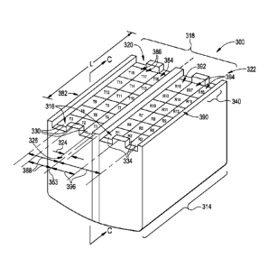
Still another example of a measurement probe 300 is illustrated in FIGS. 5-6.
Here,
as with the example of the measurement probe 200 of FIGS. 3-4, like numerals
are
used to designate like components in the measurement probe 300, but that the
numerals in FIGS. 5-6 are increased by 100. For example, it is seen in FIGS. 5-
6 that
the measurement probe 300 can include a scan area 314 with a length L,
transducer
elements 316 that can be arranged in an array 318, and more particularly in a
13
CA 02759472 2011-10-20
WO 2010/126682 PCT/US2010/030106
transmitter side 320 and a receiver side 322 that can be separated by a cross-
talk
barrier 328.
As mentioned in connection with the discussion of FIGS. 1-2 above, the
transmitter
side and the receiver side in embodiments of the measurement probes disclosed
herein
can each include, respectively, a plurality of transmitter elements 330 and a
plurality
of receiver elements 334. In the present example of FIG. 5-6, it is seen that
the
transmitter elements 330 (labeled Tl-T18) are arranged in a transmitter grid
382.
More particularly, each of the active groups 340 can include an inner
transmitter
element 384 proximate the gap 326, and at least one outer transmitter element
386
that is located an outer distance 388 that is measured from the longitudinal
axis 353.
The receiver elements 334 (labeled Rl-Rl8) are likewise arranged in a receiver
grid
390 so that each of the active groups 340 includes an inner receiver element
392 that
is separated from the inner transmitter element 384 by the spaced relationship
324.
The active group 340 also includes at least one outer receiver element 394
that is
located an outer distance 396 from the longitudinal axis 353.
When the measurement probe 300 is implemented in a system, such as the system
102
of FIG. 1, each of the transducer elements 316 that are found in the
transmitter grid
382 and the receiver grid 390 can be operated individually. In one example,
the
transmitter element Ti can be activated to transmit the ultrasound beam, and
the
receiver element RI can be activated to receive the echo signal that
corresponds to
that ultrasound beam. In another example, the transmitter elements T 1-T6 can
be
activated so as to transmit ultrasound beams, and the receiver elements RI-R6
can be
activated to receive the echo signal that correspond to those ultrasound
beams.
Nevertheless, the combinations of the transmitter elements 330 and the
receiver
elements 334 that are activated are limited only by the number of the
transducer
elements 316 that are found in the transmitter grid 382 and the receiver grid
390.
Embodiments of the measurement probe 300 are also configured so that certain
ones
of the transducer elements 316 can undergo controlled-excitation so as to
manipulate
the parameters of the ultrasound beam that is directed into the test object,
e.g., test
object 108 (FIG. 1). These parameters include, but are not limited to, the
direction,
14
CA 02759472 2011-10-20
WO 2010/126682 PCT/US2010/030106
the angle, the focal distance, and the focal spot size of the ultrasound beam.
These
terms are generally recognized by those artisans having ordinary skill in the
art, and
so these terms will not be defined or described herein, but rather referred to
in context
of the concepts of the embodiment of the measurement probes disclosed and
contemplated in the present disclosure. For example, and by way of non-
limiting
example, it is contemplated that the direction of the ultrasound beam can be
manipulated by varying the time at which each of the transmitter elements 330
is
excited with respect to the other transmitter elements in the transmitter grid
382.
Other embodiments of the measurement probe 300 are further configured so that
the
transducer elements 316 can undergo controlled-excitation so that the
measurement
probe 300 exhibits certain operational characteristics that are consistent
with the
characteristics of phased array ultrasonic technology. One exemplary
operational
characteristic includes being configured to excite one or more of the
transmitter
elements 330 so as to generate the ultrasound beam in accordance with certain
beam-
scanning patterns, such as, for example, electronic scanning, dynamic depth
focusing,
and azimuthal scanning. By way of non-limiting example, it is contemplated
that the
embodiments of the measurement probe 300 can have operational characteristics
that
are consistent with "1.25D," "1.5D," "1.75D," and "2D" transducer arrays.
Again, as
discussed in connection with the parameters of the ultrasound beam immediately
above, the control structure, instrumentation, and other considerations that
are
required to achieve such patterns will be recognized by those artisans
familiar with
phased array ultrasonic technology, and so will not be discussed herein.
However, for
purposes of example only, as used herein, the "1.25D" transducer provides a
variable
elevation aperture, with static focusing; the "1.5D" transducer array provides
a
variable elevation aperture, shading, and focusing that is symmetric about the
centerline of the array; the "1.75D" transducer array provides variable
elevation
aperture, shading, and focusing that is not symmetric about the centerline of
the array;
and the "2D" transducer array provides full electronic focusing and steering.
Discussing the operation of measurement probes that are made in accordance
with one
or more embodiments of the present invention, FIG. 7 illustrates a method 400
for
measuring the thickness of a test object using the measurement probe, e.g.,
CA 02759472 2011-10-20
WO 2010/126682 PCT/US2010/030106
measurement probes 100, 200, 300 (collectively, "the probe"). Here, the method
400
may include, at step 402, selecting a parameter, e.g., a first parameter, for
the
ultrasound beam. This may include, for example, at step 404 setting the number
of
transmitter elements and the number of receiver elements for the active groups
of the
scan area. Then, the method 400 may include, at step 406, collecting data by
interrogating the surface of the test object with the probe. Generally, this
can be
accomplished by placing the scan surface of the probe against the surface of
the test
object, and then moving the probe across the surface in a direction that is
substantially
perpendicular to the scan area. This may be repeated any number of times if
the
entire surface of the test object is to be scanned, or it can be repeated only
as
necessary based on the size of the area of interest of the test object.
After interrogating the inner volume of the test object, or alternatively
after
interrogating only a portion of the inner volume, the method 400 next may
include, at
step 408, determining if the parameter achieved the objectives of the test.
This can
include evaluating the information that is displayed by the test instrument
including,
for example, examining the resolution of an image of the test object on the
test
instrument, and/or comparing the image to a known good image that has the
resolution that is desired. If the resolution is adequate to meet the
objectives of the
test, then the method may include at step 410 finalizing the scan of the test
object,
and, at step 412, moving to a different location on the surface of the test
object.
If the resolution is not adequate, then the method can return to step 402,
selecting a
parameter for the ultrasound beam, and another parameter, e.g., a second
parameter, is
selected by, e.g., changing the number of the transmitter elements and the
number of
the receiver elements for the active groups of the scan area. In the present
example,
the probe is used to scan the surface using the second sound field
characteristic, and it
is determined if the second sound field characteristics achieve the objective
of the test.
If the resolution is not adequate, then the method 400 can continue, e.g., in
accordance with steps 402-408, until the resolution meets the objectives of
the test.
Then, as discussed above, the method 400 may include at step 410 finalizing
the scan
of the test object, and at step 412, moving to a different location on the
surface of the
test object.
16
CA 02759472 2011-10-20
WO 2010/126682 PCT/US2010/030106
This written description uses examples to disclose the invention, including
the best
mode, and also to enable any person skilled in the art to make and use the
invention.
The patentable scope of the invention is defined by the claims, and may
include other
examples that occur to those skilled in the art. Such other examples are
intended to be
within the scope of the claims if they have structural elements that do not
differ from
the literal language of the claims, or if they include equivalent structural
elements
with insubstantial differences from the literal language of the claims.
17