Note: Descriptions are shown in the official language in which they were submitted.
CA 02759586 2011-10-21
52966-56
1
An Input Converter for a Hearing Aid and Signal Conversion Method
Field of the Invention
The present invention relates to hearing aids. The invention, more
specifically,
relates to analog-to-digital input signal converters in digital hearing aids.
The
invention further relates to a method of converting an analog signal to a
digital signal
in a hearing aid.
Background of the Invention
An analog-to-digital converter, denoted an A/D converter in the following,
converts a
varying current or voltage into a digital data format. Several different A/D
converter
topologies exist, each having benefits and tradeoffs in terms of conversion
speed,
accuracy, quantization noise, current consumption, word length, linearity and
circuit
complexity. In contemporary, digital hearing aid designs, the delta-sigma A/D
converter type is the preferred converter type due to a number of important
factors
such as easy aliasing filter implementation, conversion noise being
controllable by
design, comparatively low power consumption and relatively easy implementation
due to a low component count when compared to existing A/D converter designs.
By definition, noise inherent in a signal processing device is unwanted
signals
introduced by the signal processing device itself. Inherent noise may e.g.
originate
from inadequate operating conditions, poor design or variations in component
values.
These circumstances have to be taken into account in designing the signal
processing device. In A/D converters, several different types of noise may be
observed. Among these are conversion noise, quantization noise, thermal noise,
flicker noise, recombination noise, and noise due to various physical
limitations in the
gain-producing elements. In order to provide a distinction between the sources
of
these different noise types, the most important noise types will be discussed
briefly in
the following.
CA 02759586 2011-10-21
52966-56
2
Quantization noise originates from the process of quantifying a continuous
input
voltage span into a finite set of voltage levels that may be represented by
discrete,
binary levels according to the expression:
LN = 2"
where LN is the number of discrete levels possible and n is the number of bits
used to
represent a single sample in the digital domain. Quantization noise may be
thought
of as the difference between the actual input voltage of a single sample and
the
discrete voltage used to represent it. This type of noise may thus be
minimized, e.g.
by increasing the number of bits representing the signal arbitrarily, and will
therefore
not be discussed further here.
Thermal noise originates from the random Brownian motion of electrons in a
resistive
medium. Given a resistance, a bandwidth and a temperature, the rms thermal
noise
Vnt is given by:
V. = 4k6 T Af R
where kb is Boltzmann's constant, 1,38065*10"23 J/K, T the absolute
temperature in K,
Af the bandwidth of interest in Hz and R the resistance in S2 of the circuit
element
considered.
Flicker noise, or 1/f noise, is predominant in the noise spectrum at low
frequencies. It
has been observed in electronic devices since the era of vacuum tubes, and is
also
present in contemporary semiconductor devices.
Shot noise is the result of stochastic phenomena caused by an electric current
crossing
a potential barrier, such as the barrier found between P-doped and N-doped
material in
a semiconductor element. Current shot noise In is a temperature-independent
quantity,
and may be described by the expression:
Iõ = 2q I
CA 02759586 2011-10-21
52966-56
3
where q is the electron charge, 1,602*10-19 Coulombs, and I the bias current
for the
semiconductor element. The unit of the spectral density of shot noise is A/ Hz
.
In order to provide a hearing aid capable of working uninterrupted for several
days
without a need for replacing the battery, one design goal for the hearing aid
is that the
current drawn from the battery by the electronic circuit is reduced as much as
possible, preferably to a value below 1 mA. A semiconductor element providing
amplification in the order of between one hundred times to perhaps a thousand
times
the signal present at its input uses a considerable percentage of this current
as its
bias current in order to handle the large gain within its operating limits.
From the
foregoing it is evident that shot noise is dependent on the current flowing
through the
semiconductor element, this fact providing further motivation for reducing the
bias
current for the amplifier in the A/D converter as much as possible.
Delta-sigma A/D converters are well known in the art. Their purpose is to
convert a
varying, analog input voltage into a binary bit stream for further processing
in the
digital domain. Delta-sigma A/D converters have significant advantages over
other
A/D converter designs. They have a relatively low component count, and they
feature various signal processing advantages above other A/D converter
designs. In
order to reduce conversion noise, oversampling is used. By measuring each
discrete
voltage many times, e.g. 64, errors due to statistical variations in the input
signal are
leveled out, and the conversion noise spectrum is pushed far beyond the
Nyquist
limit, thus making conversion noise very easy to filter out from the signal.
One
drawback is that the converter clock rate in this example has to be 64 times
the
desired sample clock rate.
In its essence, a delta-sigma A/D converter comprises a delta-sigma modulator
and a
low-pass filter. This may be made with an integrator, a comparator and a D-
flip-flop.
The output signal of the flip-flop is fed back through a feedback loop
comprising a
one-bit D/A converter, and is subtracted from the input signal upstream of the
integrator. The subtracted feedback signal provides an error signal to the
input of the
delta-sigma modulator.
CA 02759586 2011-10-21
52966-56
4
The error signal from the feedback loop of the A/D converter is used to ensure
that,
on average, the output signal level of the converter is always equal to the
input signal
level. If no signal is present on the converter input, a symmetric output bit
stream of
binary ones and zeroes is generated by the A/D converter. When the input
signal
voltage changes to a more positive voltage, more binary ones will be present
in the
output bit stream, and when the input signal voltage changes to a more
negative
voltage, more binary zeroes will be present in the output bit stream. The
delta-sigma
A/D converter thus converts an analog input signal into a balance between ones
and
zeroes in the output bit stream.
Summary of the Invention
The invention, in a first aspect, provides an input converter for a hearing
aid, said
converter comprising a first voltage transformer and an analog-to-digital
converter of
the delta-sigma type, the analog-to-digital converter having an input stage
and an
output stage, a connection from the output of the input stage to the input of
the output
stage, and a feedback loop between the input of the input stage and the output
of the
output stage, said input stage comprising an amplifier and an integrator,
wherein the
first voltage transformer has a transformation ratio such that it provides an
output
voltage larger than the input voltage and is placed in the input converter
upstream of
the input stage.
The invention, in a second aspect, provides a method of converting an analog
signal
into a digital signal in a hearing aid comprising a digital signal processor,
a sampling
clock generator and a system clock generator, said method comprising the steps
of
transforming an input signal voltage, amplifying the transformed input signal
voltage,
integrating the transformed, amplified voltage, digitizing the amplified,
integrated
voltage, transforming the digitized, integrated voltage into a higher voltage,
subtracting the transformed, digitized voltage from the transformed input
voltage, and
using the digitized, integrated voltage for generating a digital output bit
stream
representing the input signal voltage to subsequent stages of the digital
signal
processor in the hearing aid.
CA 02759586 2011-10-21
52966-56
In order to overcome the above shortcomings, the input converter according to
the
invention comprises a first voltage transformer placed in the input converter
upstream of
the input stage and having a transformation ratio such that it provides an
output voltage
larger than the input voltage. When the input signal voltage is transformed up
prior to
5 being amplified by the amplifier stage, less amplification is needed in
order to bring the
input signal up to an acceptable level, and the relative amplifier noise
contribution to the
amplified signal is lower, and the same is the case when the feedback signal
voltage is
transformed up prior to being presented to the amplifier input.
According to the invention, both the input transformer and the feedback
transformer
are implemented as voltage transformers. Voltage transformers are easily
implemented in synchronized (clock-controlled) digital networks, and may be
designed so as to optimize their impedance to the impedance of the amplifier
and the
subsequent stages of the A/D converter.
Further features and advantages are evident from the dependent claims.
Brief Description of the Drawings
The invention will now be described in further detail with respect to the
drawings,
where
Fig. 1 is a schematic of a prior art delta-sigma A/D converter;
Fig. 2 is a more detailed schematic of the prior art delta-sigma converter in
fig. 1;
Fig. 3 is an equivalent schematic illustrating the noise level voltage Vn of
an amplifier
of the delta-sigma converter in fig. 2;
Fig. 4 is a schematic illustrating the principle of equivalent transformation
of the input
signal to the amplifier in fig. 3;
Fig. 5 is a schematic illustrating a first phase of a prior art sampled
capacitor
integrator;
CA 02759586 2011-10-21
52966-56
6
Fig. 6 is a schematic illustrating a second phase of a prior art sampled
capacitor
integrator;
Fig. 7 is a schematic illustrating a first phase of the sampled capacitor
integrator
according to an embodiment of the invention;
Fig. 8 is a schematic illustrating a second phase of the sampled capacitor
integrator
according to an embodiment of the invention;
Fig. 9 is a schematic of an implementation of an input transformer in a first
phase
according to an embodiment of the invention;
Fig. 10 is a schematic of an implementation of an input transformer in a
second
phase according to an embodiment of the invention;
Fig. 11 is a schematic of a delta-sigma analog-to-digital converter according
to an
embodiment of the invention;
Fig. 12 is a schematic of a preferred embodiment of a delta-sigma analog-to-
digital
converter according to an embodiment of the invention; and
Fig. 13 is a schematic of a hearing aid having four delta-sigma converters
according
to an embodiment of the invention.
Detailed Description of the Preferred Embodiments
Fig. 1 shows a block schematic of a prior art delta-sigma A/D converter
comprising an
input terminal IN, a subtraction point 1, an integrator 2, a comparator 3, a D-
flip-flop 4,
a 1-bit digital-analog converter 5, a clock generator 6, and an output
terminal OUT. An
analog signal presented to the input terminal IN is fed to the subtraction
point 1 where
the output signal from the 1-bit D/A converter 5 is subtracted from the input
signal,
generating an error signal. The difference signal from the subtraction point 1
is fed to
the input of the integrator 2 for generating an integral of the difference
signal from the
subtraction point 1. The output signal from the integrator 2 is presented to
the input of
the comparator 3 for generating a logical "one"-level whenever the integral
signal
CA 02759586 2011-10-21
52966-56
7
exceeds a predetermined threshold limit set by the comparator 3, and a logical
"zero"-level whenever the output signal from the integrator 2 falls below the
predetermined threshold. This logical signal then feeds the data input of the
flip-flop 4.
The clock generator 6 controls the flip-flop 4 in such a way that the output
signal from
the comparator 3 is quantized in time and synchronized to the clock signal,
the
flip-flop 4 working as a latch, thus creating a bit stream representing the
input signal.
The bit stream from the output of the flip-flop 4 is split between the output
terminal
OUT and the input of the 1-bit D/A converter 5 to the subtraction point 1 and
subtracted from the input signal. The 1-bit D/A converter 5 converts the
logical ones
and zeroes in the bit stream into a positive or negative voltage with respect
to the
input signal for subtraction from the input signal in the subtraction point 1.
This arrangement, in essence, creates a feedback loop, making the bit stream
represent the changes in the input signal over time, i.e. when the input
signal level is
zero, an equal number of digital ones and zeroes will be present in the bit
stream;
whenever the input signal goes positive, more ones than zeroes will be present
in the
bit stream in a proportion to the input signal level; and whenever the signal
goes
negative, more zeroes than ones will be present in the bit stream in a
proportion to
the input signal level. The bit stream may then be converted into a suitable,
digital
format for further processing in the digital domain.
A delta-sigma A/D converter design for a hearing aid should have a small noise
figure
and a low current consumption. However, if the current consumption of the
input
amplifier of the A/D converter is decreased without any alterations to the
design, the
noise figure of the amplifier will increase correspondingly. This problem, and
a
possible solution, will be explained in further detail in the following.
Fig. 2 shows a more detailed schematic of a prior art delta-sigma A/D
converter. The
converter comprises an input IN, a first resistor R1, a second resistor R2, an
amplifier
A, a capacitor C, a residual loop filter RLF, a D-flip-flop DFF, and a clock
generator
CLK generating a clock signal. The amplifier A and the capacitor C forms the
integrator 2 of the converter topology shown in fig. 1, and the residual loop
filter RLF
CA 02759586 2011-10-21
52966-56
8
comprises subsequent low-pass filter stages present in second- or higher-order
delta-sigma converters. The converter receives an analog input signal in the
form of
a voltage U at the input terminal IN and presents a bit stream representing a
digital
output signal Y at the output terminal OUT. It should be noted that the
signals in the
converter are time-continuous until the generation of the bit stream from the
output Q
of the flip-flop DFF.
The amplifier A and the residual loop filter RLF comprises the loop filter of
the
converter, and the frequency transfer function of the loop filter, i.e. the
frequency
transfer function of both A and RLF, determines the converter's ability to
suppress
frequency-dependent quantization noise. The gain of the amplifier A also
suppresses
the noise from the filter RLF because the filter RLF is positioned in the
feedback loop
of the converter. In this discussion, the reason for distinguishing between
the amplifier
loop filter, respectively, is to isolate the noise contribution from the
amplifier A from
other noise sources in the feedback loop. All other things being equal, the
noise level
of the amplifier A thus constitutes the main noise component of the converter
apart
from quantization noise. This is the reason that the contribution from this
particular
noise source should be minimized, as mentioned in the foregoing.
If the amplifier A were to have infinite gain, the signal level on the input
terminal of the
amplifier would be zero. Instead it may be assumed that the total gain of A
and RLF
combined is sufficiently large throughout the desired frequency bandwidth of
the
converter for the converter quantization noise to be neglected. Given an input
voltage U and a resulting output voltage Y, the transfer function H of the
complete
converter in fig. 2 in the ideal case may thus be estimated as:
H=Y=-R2
U R1
In order to address the problem of the noise contribution from the input stage
of the
converter, this particular noise source has to be isolated. This is
illustrated in the
schematic in fig. 3.
CA 02759586 2011-10-21
52966-56
9
In fig. 3, an ideal, noise-free amplifier A and a noise voltage source Vn is
substituting
the amplifier A in fig. 2, and the configuration of C, R1, R2 and A is
sketched out
together with the input voltage U, the output voltage Y, and the amplifier
noise
voltage source Vn, while the remaining components from fig. 2 are left out
from the
schematic for clarity. If the total amplification from A and RLF (not shown in
fig. 3) is
assumed to be sufficient for the desired bandwidth of the converter, the noise
contribution Yn to the output voltage Y may be written as:
Yn=[1+Rl}.Vn
The noise voltage contribution Un with reference to the input voltage U may
then be
calculated by combining the two expressions thus:
Un = H. =-Cl+R2)'Vn
This implies that the input noise Un is dependent on the amplifier noise Vn.
In other
words, if it is possible to decrease Vn, the input noise Un will decrease,
too.
The amplifier noise voltage Vn has three primary origins. Noise due to the
fact that
the amplifier A has finite gain, intermodulation products originating from
nonlinearities
in the amplifier A, and thermal noise produced by the input stage of the
amplifier A.
Multi-stage amplifiers with large gain values have traditionally been used in
order to
minimize thermal noise. Likewise, noise may also be reduced by supplying the
semiconductor elements in the amplifier with sufficiently large currents in
order to
keep the total noise in the output signal at an acceptable level.
However, none of these approaches are especially attractive in a converter
design for
a hearing aid, where current consumption and component count has to be kept to
a
minimum in order to prolong battery life. An alternative way of reducing the
noise
sensitivity of the amplifier in the converter is thus desired.
CA 02759586 2011-10-21
52966-56
In theory, the noise voltage Vn may be downscaled, e.g. by transforming the
input
signal U and the output signal Y by placing ideal transformers between the
input
terminal U and R1 and between the output terminal and R2 with a given
transformation factor N.
5 Fig. 4 shows an equivalent schematic of the converter in fig. 3 as modified
by the
incorporation of ideal transformers T1 and T2 in the input branch and the
output
branch of the converter, respectively. The input transformer T1 transforms the
input
voltage by the ratio 1:N, (i.e. the voltage on the transformer output is N
times the
voltage on the transformer input), and the feedback transformer T2 transforms
the
10 feedback voltage by the ratio 1:N (i.e. the voltage presented to the
amplifier is N
times the voltage present at the output node Y). The values of the resistors
R1 and
R2 are each scaled with a factor of N2 in order to preserve the current load
of the
input and the output, respectively. Likewise, the value of the integrator
capacitor C is
scaled by the factor N 2. It may be shown that the resulting amplifier noise
voltage Vn
is scaled correspondingly by the factor Vn/N. In theory, it is possible to
scale the
noise contribution from the amplifier stage down by an arbitrary amount,
providing the
amplifier stage is capable of handling the increased input voltage without
being
saturated. The current demands for the converter are also smaller due to the
impedance transformation.
Real transformers are non-ideal and therefore impossible to use in practical
hearing
aids due to their size, weight, current consumption and power losses. The
inventor
has realized that the equivalent of an ideal transformer may be applied as a
solution
to the problem with satisfactory results. Such an equivalent is described in
further
detail in the following. The starting point of this discussion is a delta-
sigma A/D
converter utilizing a topology based on sampled capacitors. Sampled-capacitor
stages are considered to be well-known in the art, and the working principle
of such a
sampled-capacitor A/D converter is described in further detail in the
following with
reference to fig. 5 and fig. 6.
CA 02759586 2011-10-21
52966-56
11
Fig. 5 is a schematic illustrating a first phase of a sampling clock control
signal in a
prior art sampled-capacitor delta-sigma A/D converter comprising an input
terminal U,
a first sampling capacitor Cs, a first switch S1, a second switch SE, a hold
capacitor
Ch, an amplifier A, a feedback loop capacitor Cs', a feedback loop terminal Q
and an
output terminal Y. The feedback loop terminal Q carries the feedback signal
from the
output of the D-flip-flop (not shown). The switches S, and SE are controlled
by a
sampling clock (not shown). In a first phase of the sampling clock control
signal,
shown in fig. 5, the sampling capacitor Cs is charged by the input voltage
presented
on the input terminal U during a first, specific period of time, via the
switch S,. The
second switch SE is open in the first phase.
In a second phase of the sampling clock control signal, shown in the schematic
in
fig. 6, the switch S, disconnects the sampling capacitor Cs from the input
terminal U
and connects it to the input of the amplifier A and the hold capacitor Ch,
whereby the
sampling capacitor CS is discharged for a second, specific period of time via
the
switch Si, transferring its charge to the hold capacitor Ch. The switch SE is
closed in
the second phase, and connects the feedback loop capacitor CS' to the input of
the
amplifier A. The voltage on the input terminal of the amplifier A is now equal
to the
voltage on the input terminal U during the first period of time minus the
error voltage
present on the feedback terminal Q. When the second phase ends, the switches
S,
and SE are returned to their initial positions shown in fig. 5, and the
process is
repeated periodically.
If the position of the switch S is controlled by a periodical signal having
the frequency
fs, the impedance Zs of the sample capacitor Cs may be described as:
1
Zn (CS'
Consider the sampling capacitor Cs of the sampled-capacitor delta-sigma A/D
converter in the first phase shown in fig. 5 split into two capacitors, each
having a
capacitance of Cs/2. A voltage transformation may then be implemented by
changing
the sampled-capacitor design to look like the schematic in fig. 7 and fig. 8,
CA 02759586 2011-10-21
52966-56
12
respectively. The sampled-capacitor circuit design shown in fig. 7 and fig. 8
comprises two controlled switches S, and SE, an amplifier A, a hold capacitor
Ch, and
four capacitors Ca and Cb, Cc and Cd, each of the four capacitors having a
capacitance of CS/2. In fig. 7, the switch S, connects the two capacitors Ca
and Cb to
the input terminal IN in parallel in the first phase, in a manner similar to
that shown in
fig. 5, and in fig. 8, the switch S, connects the two capacitors Ca and Cb to
the
amplifier A in series in the second phase in a manner similar to that shown in
fig. 6.
Likewise, the feedback capacitors Cc and Cd are charged in parallel to the
voltage
present on the feedback loop terminal Q with reference to ground via the
switch SE in
the first phase in fig. 7, and in the second phase, shown in fig. 8, the
feedback
capacitors Cc and Cd are connected in series between the feedback loop
terminal Q
and the amplifier A via the switch SE during discharge of the feedback
capacitors Cc
and Cd, whereby the voltage drop between the feedback loop terminal Q and the
hold
capacitor Ch is doubled. The voltage present at the input of the amplifier A
in the
second phase is then Vu - VQ, i.e. the doubled input voltage minus the doubled
feedback voltage.
The effect of this arrangement is that the input node of the amplifier A is
isolated from
the input terminal U and the feedback loop terminal Q by the voltage
transformers
formed by the capacitors Ca, Cb, Cc and Cd, respectively. The net result of
doubling
the input voltage and the feedback loop voltage is that the intrinsic noise
level Vn of
the amplifier A becomes comparatively smaller, and the signal-to-noise ratio
thus is
improved, while maintaining both the input impedance and the output impedance
of
the amplifier stage A as seen from outside the circuit shown in fig. 7 and
fig. 8,
respectively.
With the capacitors Ca, Cb, Cc and Cd having values of CS/2, respectively,
this
configuration is equivalent to a voltage transformation with a transformation
factor
of 1:2 for the input transformer, respectively 2:1 for the feedback
transformer, as the
impedance ZS of the hold capacitor C. now becomes:
CA 02759586 2011-10-21
52966-56
13
4
Zs =
(CS-f')
This arrangement thus effectively quadruples the input impedance of the
amplifier A.
By changing the configuration of the circuit in synchronization with the two
phases of
the sampling clock frequency fs of the sampled-capacitor delta-sigma A/D
converter,
by means of the switches S, and SE as shown in fig. 7 and 8, the input voltage
U
presented to the input terminal of the amplifier A is then doubled to 2U.
Consider the amplifier A having unity gain, and an error signal of 0 V being
present
on the feedback loop terminal Q. Then the output signal downstream of the
second
voltage transformer Cc and Cd is:
2=U+Vn =U+Vn
2 2
This is based on the imperative that the capacitors Cc and Cd are shifted
between the
parallel configuration in the first phase shown in fig. 7 and the serial
configuration in
the second phase shown in fig. 8. By isolating the input of the amplifier A of
the input
stage of the A/D-converter from the rest of the circuitry with first and
second voltage
transformers in this way, an effective, comparative noise figure of Vn/2 may
be
obtained in a simple and effective manner.
A schematic illustrating a first and a second phase of the function of the
input voltage
transformer circuit of fig. 7 and 8 is described in the following with
reference to fig. 9
and fig. 10. In fig. 9 and fig. 10, a voltage transformer circuit comprises an
input
terminal U, an output terminal VA, five controlled switches S1, S2, S3, S4,
and S5,
and two sampling capacitors Ca and Cb, both having a capacitance of Cs/2 with
respect to the schematic of the circuit shown in fig. 5 and 6. The output
terminal VA
of the voltage transformer circuit is to be connected to an amplifier (not
shown) as
illustrated in fig. 7 and 8.
CA 02759586 2011-10-21
52966-56
14
In the first phase of the voltage transformer, shown in fig. 9, the switches
S1, S3, and
S5 are closed, and the switches S2 and S4 are open. The two capacitors are
thus
connected in parallel to the input terminal U in fig. 9. A voltage present on
the input
terminal U will thus charge the capacitors Ca and Cb to the same voltage.
In the second phase of the voltage transformer, shown in fig. 10, the switches
S1, S3,
and S5 are now open, and the switches S2 and S4 are now closed. The two
capacitors Ca and Cb are now connected in series, thus doubling their total
charge
voltage while reducing the total capacitance to CS/4, and connected to the
output
terminal VA. The combined charge collected by the capacitors Ca and Cb is now
presented as a voltage to the output terminal VA. This voltage is double the
voltage
of U due to the altered configuration of the capacitors Ca and Cb.
Consider the output terminal VA of the input voltage transformer shown in fig.
9 and
fig. 10 connected to the input stage of an amplifier A in the way shown in
fig. 7 and
fig. 8. If the amplifier A has an amplification gain 13, then the input
voltage U is both
doubled and multiplied by (3, but the noise voltage Võ is just multiplied by
P. For a
given input voltage U, the voltage output Vy from the amplifier A will be:
VY =2. 3.U+P.V,, b V, =P(2=U+Võ)
The noise voltage contribution Vn to the output voltage Vy is then half the
noise
voltage contribution of the untransformed input voltage in this case, provided
that the
amplifier is capable of handling the transformed input voltage of 2U.
The voltage contribution from the feedback loop signal of the delta-sigma A/D
converter is doubled in a similar way by the second voltage transformer Cc and
Cd as
indicated in fig. 7 and fig. 8.
The principle of voltage transformation is extensible to an arbitrary number N
of
sampling capacitors each having the capacitance of CS/N, in effect reducing
the
apparent noise figure of the amplifier equally to Võ/N. It is not essential
for operation
CA 02759586 2011-10-21
52966-56
of the invention that the input transformer and the feedback transformer have
the
same transformation ratio. This principle permits implementation of the input
amplifier in a much simpler way due to the reduced demands on its performance
with
regard to amplification gain, thermal noise, intermodulation noise, and errors
due to
5 finite gain of the amplifier.
The amplifier in the input stage of the A/D converter according to the
invention may
consequently be implemented as a simple, single-stage amplifier comprising one
single semiconductor element, such as a BJT, FET, or other amplifying element
having sufficient gain. Single-stage amplifiers inherently have a very
attractive
10 relationship between thermal voltage noise and current consumption. The
voltage
transformation further reduces the bias current demands of the amplifier and
thus the
current consumption of the complete A/D converter, of which the bias current
for the
input amplifier constitutes a substantial part.
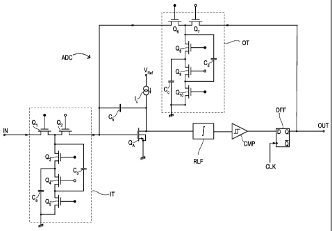
Fig. 11 shows a delta-sigma A/D converter ADC according to the invention. The
A/D
15 converter ADC comprises an input terminal IN, an input transformer stage
IT, an
amplifier stage QA, a hold capacitor Ch, a constant current generator I., a
feedback
transformer stage OT, a residual loop filter RLF, a comparator CMP, a flip-
flop DFF,
and an output terminal OUT. The flip-flop DFF is controlled by a system clock
source
(not shown). The amplifier stage QA is fed a constant current from the
constant
current source IC powered by a connection to the reference voltage source
Vfef. This
current controls the operating point of the amplifier QA in order for it to be
able to
provide the desired gain to the input signal.
The input transformer stage IT comprises switching transistors Q1, Q2, Q3, Q4,
and Q5,
and capacitors Ca and Cb. The feedback transformer stage OT comprises
switching
transistors Q6, Q7, Q8, Q9 and Q1o, and capacitors Cc and Cd. For simplicity,
these four
capacitors are considered to be of equal capacitance, i.e. Ca= Cb=Cc=Cd.
CA 02759586 2011-10-21
52966-56
16
The switching transistors Q1, Q2, Q3, Q4 and Q5 of the input transformer stage
IT are
controlled by a sampling clock generator (not shown) in such a manner that
when the
signal edge of the sampling clock generator goes positive in a first phase,
the
switching transistors Q1, Q3, and Q5 close (i.e. they allow an electrical
current to
pass), and Q2 and Q4 open (i.e. they block an electrical current). This is
illustrated in
fig. 11 by an open or a filled circle, respectively, on the base terminal of
the
respective switching transistors. In the first phase of the signal edge of the
sampling
clock generator, a filled circle denotes a closed transistor and an open
circle denotes
an open transistor.
When the signal edge of the sampling clock generator goes negative in a second
phase, the switching transistors Q1, Q3, and Q5 of the input transformer IT
open, and
the switching transistors Q2 and Q4 close. In the second phase of the signal
edge of
the sampling clock generator, an open circle denotes a closed transistor and a
filled
circle denotes an open transistor. This configuration is equivalent to the
schematics
shown in figs. 9 and 10, respectively, where the transistors Q1, Q2, Q3, Q4,
and Q5
substitute the switches S1, S2, S3, S4, and S5, respectively, retaining the
essential
function of the circuit shown in figs. 9 and 10. The clock frequency of the
sampling
clock generator (not shown) is of the magnitude of 30 kHz, and the clock
frequency of
the system clock generator (not shown) is of the magnitude 1-2 MHz. This gives
an
oversampling ratio of the converter of from 30 to 60 times oversampling.
In the first phase, where Q,, Q3 and Q5 are closed and Q2 and Q4 are open, the
capacitors Ca and Cb are connected in parallel to the input terminal IN, and
each
capacitor is charged to the voltage present on the input terminal IN. In the
second
phase, where Q1, Q3 and Q5 are open and Q2 and Q4 are closed, the capacitors
Ca
and Cb are connected in series to the input of QA, delivering their combined
charge to
the input of QA and the hold capacitor Ch. Due to this arrangement, the input
voltage
fed to the input transformer IT will be doubled at its output, as explained
above.
CA 02759586 2011-10-21
52966-56
17
The switching transistors Q6, Q7, Q8 Q9 and Q10 of the feedback transformer OT
are
also controlled by the sampling clock generator (not shown) in such a way that
when
the signal edge of the sampling clock generator goes positive in the first
phase, the
switching transistors Q6, Q8 and Quo close and Q7 and Q9 open. This is also
illustrated by an open or a filled circle, respectively, on the base terminal
of the
respective switching transistors, where a filled circle denotes a closed
transistor and
an open circle denotes an open transistor. This implies that the capacitors Cc
and Cd
are connected in parallel to the input of the amplifier QA in the first phase,
delivering
their combined charge to the input of the amplifier QA.
In the second phase, when the signal edge of the sampling clock generator goes
negative, the switching transistors Q6, Q8 and Qjo open, and Q7 and Q9 close.
In this
case, an open circle on the base terminal of the respective transistor denotes
a
closed transistor and a filled circle denotes an open transistor. This implies
that the
capacitors Cc and Cd are connected in series to the output terminal OUT in the
second phase and charged by the error voltage from the flip-flop DFF. The
capacitors Cc and Cd are essentially placed in the feedback loop of the
amplifier QA,
doubling the feedback voltage from the output of the flip-flop DFF before
presenting
the error voltage to the input of the amplifier QA.
The residual loop filter RLF outputs the integral of the signal from QA, and
the
comparator CMP outputs a logical zero value whenever the integral is below a
predetermined threshold, and a logical one value whenever the integral is
above a
predetermined threshold. The flip-flop DFF converts the binary integral signal
from
the comparator CMP into a bit stream controlled by the clock signal CLK and
fed to
both the output terminal OUT and the input of the feedback transformer OT as a
feedback signal.
By doubling the voltage present at the input of the amplifier QA with the
voltage
transformers IT and OT respectively, the input voltage is increased by a
factor two,
and the relative noise voltage level Vn is reduced as a consequence without
the need
for increasing the supply current to the amplifier QA.
CA 02759586 2011-10-21
52966-56
18
An embodiment of the A/D converter according to the invention is shown in fig.
12.
The general configuration of the input terminal IN, the input transformer IT,
the
feedback transformer OT, the constant current generator Ic, the amplifier QA,
the hold
capacitor Ch, the residual loop filter RLF, the comparator CMP, the flip-flop
DFF, and
the output terminal OUT is similar to the configuration shown in fig. 11, but
the
topologies of the input transformer IT and the feedback transformer OT differs
from
the embodiment shown in fig. 11.
The input transformer IT comprises switching transistors, Q1, Q2, Q3, Q4, and
Q5, and
capacitors Ca and Cb, and the feedback transformer OT comprises switching
transistors, Q6, Q7, Q8, Q9, Quo, and Q11, one capacitor Cc, and two AND gates
AG1
and AG2. In this embodiment, the feedback transformer OT has one capacitor
less
than the embodiment shown in fig. 11.
All the switching transistors of the input transformer IT and some of the
switching
transistors of the feedback transformer OT are controlled by a sampling clock
generator (not shown) in such a way that when the sampling clock signal goes
positive in a first phase, the transistors Q1, Q2, Q5, Q7, and Qio close, i.e.
they allow
an electric current to pass, and the transistors Q3 and Q4 open, i.e. they
block an
electric current. When the clock signal goes negative, in a second phase, the
transistors Q1, Q2, Q5, Q7, and Quo open, and the transistors Q3 and Q4 close.
The switching transistors Q6, Q8, Q9 and Q11 are controlled by first and
second AND
gates AG1 and AG2, respectively. The first AND gate AG1 outputs a logical high
level
when the logical flip-flop output Q is logically high and the inverted system
clock
signal CLK is logically high. The second AND gate AG2 outputs a logically high
level when the flip-flop output Q is logically high and the system clock
signal CLK is
logically high. The logical flip-flop output signals Q and Q are mutually
exclusive,
and CLK and CLK are also mutually exclusive, so only one of the two AND gates
AG1 and AG2 may output a logically high level at any one time. When a logical
zero
is present in the bit stream, AG1 is logically high on every negative clock
pulse, and
CA 02759586 2011-10-21
52966-56
19
when a logical one is present in the bit stream, AG2 is logically high on
every positive
clock pulse.
When the first AND gate AG1 outputs a logically high level, the switching
transistors
Q6 and Q8 close, while the switching transistors Q9 and Q11 open. This has the
effect
of the first node of the capacitor Cc being connected to ground through Q8,
and the
second node of the capacitor Cc being connected to the input of the amplifier
QA, and
whatever voltage present on the first node of the capacitor Cc is mirrored as
a
negative voltage at the input of the amplifier QA. In the first phase of the
sampling
period, the switching transistors Q7 and Q10 are closed. They provide the
voltage Vref
to the first node of the capacitor Cc, and connects the second node of Cc to
ground,
while Vref gets added to the voltage already present on the first node of Cc.
In the
second phase of the sampling period, the switching transistors Q7 and Q10 are
open.
The first node of the capacitor Cc is now connected to the output of AG1, and
the
second node of Cc is connected to the input of the amplifier QA.
When the second AND gate AG2 outputs a logically high level, the switching
transistors Q9 and Q11 are closed, while the switching transistors Q6 and Q8
are open.
Consequently, the first node of the capacitor Cc is connected to the input of
the
amplifier QA, and the second node of the capacitor Cc is connected to Vref
through Q8.
In the first phase of the sampling period, the switching transistors Q7 and
Q10 are
closed. They provide the voltage Vref to the first node of the capacitor Cc,
and
connect the second node of Cc to ground while Vref gets added to the voltage
already
present on the first node of Cc. In the second phase of the sampling period,
the
switching transistors Q7 and Q10 are open. The first node of the capacitor Cc
is now
connected to the input of the amplifier QA, and the second node of Cc is
connected to
the output of AG1.
The result of this arrangement is that whenever a logical one is present in
the bit
stream to the output terminal OUT, the voltage contribution from OT is equal
to 2Vref,
and whenever a logical zero is present in the bit stream, the voltage
contribution from
CA 02759586 2011-10-21
52966-56
OT is equal to -Vref. For a bit stream comprised of an equal number of ones
and
zeroes, the mean value of the error signal from OT is thus equal to'/2Vref=
The delta-sigma A/D converter according to the invention accomplishes two
goals at
the same time. Firstly, the single-stage input amplifier design implies that
the current
5 consumption of the input amplifier may be reduced considerably, and
secondly, the
signal-to-noise ratio is improved by transforming up the signal level before
it reaches
the input stage. The application of sample-clock controlled voltage
transformers for
isolating the input stage from the input and the error feedback loop,
respectively,
provides the solution to the signal-to-noise ratio problem arising from using
a
10 single-stage input amplifier without a significant increase in power
consumption. This
design is preferred in a battery-powered circuit such as a hearing aid, and as
a result,
more than one delta-sigma A/D converter may be implemented on the circuit chip
comprising the main part of the electronic circuit of a hearing aid.
Fig. 13 is a schematic of a hearing aid 20 comprising a plurality of A/D
converters
15 according to the invention. The hearing aid 20 comprises a first microphone
21, a
second microphone 22, a telecoil 23, an antenna 24, a wireless receiver 25, a
first
A/D converter 26, a second A/D converter 27, a third A/D converter 28, a
fourth A/D
converter 29, a digital signal processor 30 and a loudspeaker 31. All the
components
of the hearing aid 20 are fed from a battery cell (not shown) disposed within
the
20 hearing aid.
When in use, the first microphone 21 and the second microphone 22 pick up
acoustical signals from the surroundings and convert them into continuously
varying
electrical signals for use by the hearing aid 20. The continuously varying
electrical
signal from the first microphone 21 is fed to the first A/D converter 26,
which converts
the variations in the electrical signal into a first digital bit stream
suitable for being
processed by the digital signal processor 30. In a similar way, the
continuously
varying electrical signal from the second microphone 22 is fed to the second
A/D
converter 27, which converts the variations in the electrical signal into a
third digital
CA 02759586 2011-10-21
52966-56
21
bit stream suitable for being processed by the digital signal processor 30. As
the first
and the second A/D converters 26 and 27 are independent entities, they
generate
individual bit streams for independent processing by the digital signal
processor 30.
The digital signal processor 30 may combine the individual bit streams from
the first
and the second A/D converters 26 and 27, representing the signals from the
first and
the second microphone 21 and 22, respectively, in such a way that directional
information inherent in the acoustical signals picked up by the microphones is
retained for processing in the digital signal processor 30 and subsequent
reproduction by the speaker 31.
In situations where a suitable wireless signal is available, the wireless
receiver 25 may
be engaged for receiving and demodulating the wireless signal for reproduction
by the
hearing aid 20. The wireless signal is received by the antenna 24, demodulated
by the
wireless receiver 25, and presented as a varying electrical signal to the
third A/D
converter 28, which converts the variations in the electrical signal into a
third digital bit
stream suitable for being processed by the digital signal processor 30. The
third A/D
converter 28 operates independently of the first A/D converter 26 and the
second A/D
converter 27, and the signal from the wireless receiver 25 may thus be
selected even if
both the first and the second microphone 21 and 22 are engaged simultaneously.
If the hearing aid user is at a location where a telecoil loop system is
present, it may be
advantageous to use the signal from the telecoil 23. In this case, signals
from the loop
system (not shown) is picked up by the telecoil 23 and presented to the input
of the
fourth A/D converter 29, which converts the variations in the electrical
signal into a
fourth digital bit stream suitable for being processed by the digital signal
processor 30.
The fourth A/D converter 29 operates independently of the first, the second
and the third
A/D converters 26, 27 and 28, respectively, and the signal may be selected
even if both
the first microphone 21, the second microphone 22, and the wireless receiver
25 are
engaged at the same time.
CA 02759586 2011-10-21
52966-56
22
The digital signal processor 30 comprises means (not shown) for selecting up
to four
individual bit streams from the four A/D converters 26, 27, 28 and 29,
respectively.
The bit streams are preferably interleaved by the digital signal processor 30
and
mutually weighted in order to generate a preferred balance between the signals
from
the four signal sources feeding the four A/D converters 26, 27, 28 and 29 for
reproduction to a hearing aid user.
The digital signal processor 30 performs a series of calculations on the
individual bit
streams in order to process the digital representations of the audio signals
according
to an individual prescription for the hearing aid user. The balance between
the signals
from the four signal sources feeding the four A/D converters 26, 27, 28 and 29
may be
determined when fitting the hearing aid to the user, and subsets of different
signal
source balances may be stored in the hearing aid as programs for later recall
by the
user.