Note: Descriptions are shown in the official language in which they were submitted.
CA 02759688 2014-01-16
1
DESCRIPTION
ANTENNA SHEET, DATA CARRIER WITH NON-CONTACT IC, AND METHOD
FOR MANUFACTURING ANTENNA SHEET
TECHNICAL FIELD
[0001]
The present invention relates to an antenna sheet, a data carrier with a
non-contact IC, and a method for manufacturing an antenna sheet.
BACKGROUND ART
[0002]
Systems using non-contact IC cards and non-contact IC tags have come into
increased use in recent years. For example, non-contact data media which are
provided
with an IC inlet capable of electronic data input or the like are used in
booklets such as
passports and bank passbooks. A non-contact data medium has an integrated
circuit (IC
chip) and an antenna that is connected to the integrated circuit, with a base
material that
is superior in tear strength to high-quality paper or coated paper and also
has good
flexibility attached to both sides of the antenna sheet.
[0003]
In general, the antenna of an antenna sheet, in addition to functioning as an
antenna for data communication, functions as a coil to generate electrical
power by
electromagnetic induction for driving the integrated circuit. For this reason,
in an
antenna sheet a band-shaped antenna is wound in a coil-like (helical) shape on
the surface
of the antenna sheet. Given this constitution, the ends of the antenna are
disposed at the
inside and outside of the coil.
[0004]
CA 02759688 2011-10-21
2
In order to connect the two ends of the antenna to the integrated circuit, it
is
necessary at least at one location to have a bridge between the inside and the
outside of
the antenna. In the usual antenna sheet, a conductive member (bridge pattern)
is
provided on the side of the sheet base material opposite from the side on
which the
antenna is formed, the inside and outside of the antenna being bridged by
making a
connection between the bridge pattern and the antenna end part and/or
connection
pattern.
[0005]
In this type of connection part between the bridge pattern and the antenna,
after
forming the bridge pattern and antenna on both sides of the sheet base
material, electrical
conductivity is established therebetween by crimping both to make a mechanical
contact
therebetween (for example, Patent Document 1). Another known method of
achieving
electrical conductivity is to provide a through hole in the sheet base
material and then
either plate the inside of the hole or fill it with a conductive member.
[0006]
Patent Document 1: Japanese Patent No. 3634774
DISCLOSURE OF INVENTION
Problem to be Solved by the Invention
[0007]
However, the following problems exist with the above-noted method.
Specifically, with connection by crimping, because the connection is made by
merely
mechanical pressure, the bonding strength at the connection part is weak, and
the
reliability as an electrical connection is low. For this reason, when heat
treating is done
after the connection is made by crimping, the difference in the coefficient of
thermal
expansion between the sheet base material and the antenna results in warping,
causing the
opening of the electrical connection and preventing a sufficient electrical
connection.
Also, with connection by crimping, because there is only a physical contact at
the
connection part, it is not possible to maintain a stable contact resistance
unless a certain
CA 02759688 2011-10-21
3
pressure is applied. Also, with connection by crimping, there is the problem
of
oxidation or corrosion of the contact surfaces. Additionally, achieving
conductivity via
a through hole complicates the process and worsens manufacturing efficiency.
[0008]
The present invention was made in consideration of the above-described
situation, and has as an object to provide an antenna sheet that prevents open
wires in the
antenna to improve reliability, lowers the electrical resistance, and also
enables an
improvement in manufacturability. Another object is to provide a data carrier
with a
non-contact IC having such an antenna sheet. Yet another object is to provide
a method
for manufacturing an antenna sheet that prevents open wires to improve
reliability, and
also enables improvement in manufacturability.
Means for Solving the Problem
[0009]
(1) To solve the above-described problem, as a first aspect of the
present
invention, there is provided a method for manufacturing an antenna sheet,
including: a
pressing step in which an overlapped portion of an antenna coil and/or a
connection
pattern formed from a metal material and provided on one surface of a
substrate formed
from a thermoplastic resin, and a conductive member formed from a metal
material and
provided on the other surface of the substrate is pressed using a pressing
unit at least from
the surface of one side of the substrate; and a welding steps in which the
overlapped
portion of the antenna coil and/or the connection pattern and the conductive
member is
welded.
[0010]
(2) In the first aspect of the present invention, in the
pressing step, the
overlapped portion of the antenna coil and/or the connection pattern and the
conductive
member may be pressed by a pressing unit that is heated to at least the
softening
temperature of the material that forms the substrate.
CA 02759688 2011-10-21
4
According to this method, in the pressing step the substrate that is
sandwiched
between the antenna coil and the conductive member is pressed by the pressing
units
while being heated to a temperature exceeding the softening temperature. For
this
reason, a melted substrate is pressed away.
[0011]
(3) In the first aspect of the present invention, in the welding steps, a
laser beam may strike a part pressed by the pressing unit to weld the antenna
coil and/or
the connection pattern to the conductive member.
According to this method, by performing the welding in the welding step by
using laser beam, the antenna coil and/or the connection pattern and the
conductive
member are welded and securely connected. Because laser welding is a non-
contact
process, in contrast to a contact-type process in which soiling or wearing of
a fixture
influences the bonding quality, it is possible to achieve a bonding condition
with stable
quality. Also, because there is no fixture replacement required, it is
possible to achieve
a high production efficiency.
[0012]
(4) In the first aspect of the present invention, in the welding step, a
hole may be formed at the location that is struck by the laser beam.
According to this method, the strength of the bond between the antenna coil
and/or the connection pattern and the conductive member made via the through
hole is
greatly strengthened after lamination. By detecting whether or not a through
hole is
formed at the location at which the laser beam strikes, it is possible to
judge whether or
not welding has been done between the antenna coil and/or connection pattern
and the
conductive member, thereby facilitating a check for a poor connection.
[0013]
(5) In the first aspect of the present invention, the method for
manufacturing an antenna sheet may further include a mounting step in which
the
antenna coil and an integrated circuit are connected.
CA 02759688 2011-10-21
By doing this, the antenna coil and the integrated circuit are connected,
thereby
enabling the manufacture of the IC inlet.
[0014]
In general, integrated circuits such as IC chips are more expensive than other
members. For this reason, by mounting the integrated circuit after connecting
the
antenna coil and/or connection pattern and the conductive member, it is
possible to
reduce the loss incurred by a failure occurring as a poor connection between
the antenna
coil and/or connection pattern and the conductive member.
[0015]
In this context, the term "integrated circuit" encompasses not only an IC
chip,
but also a resin seal in which an IC chip is sealed, or a lead frame to which
an IC chip is
mounted, the combination of which with the IC chip is an IC module.
[0016]
(6) In a second aspect of the present invention, there is provided an
antenna sheet including: a substrate; a band-shaped antenna coil formed in the
shape of a
helix on one surface of the substrate; and a conductive member provided so as
to extend
on the other surface of the substrate in a direction that intersects with the
antenna coil,
and, when seen in plan view, to overlap with at least one end part of the two
end parts of
the antenna coil, wherein at least a part of a contacting part between the
conductive
member and one end of the antenna coil and/or connection pattern is welded.
According to this constitution, the antenna coil and/or connection pattern and
the
conductive member that are mounted on both sides of the substrate are securely
connected physically, enabling an antenna sheet having a high, stable
electrical reliability
as well.
[0017]
(7) In the second aspect of the present invention, the conductive
member and the antenna coil and/or connection pattern may cover a through hole
provided in the substrate and make mutual contact at the inner wall of the
through hole.
CA 02759688 2011-10-21
6
According to this constitution, it is possible to provide an antenna sheet
with
high reliability.
[0018]
(8) In the second aspect of the present invention, a hole may be
formed at the welded portion of one end of the antenna coil and/or the
connection pattern
so as to pass mutually therethrough, and the conductive member and the antenna
coil
and/or connection pattern may be melted at the inner wall of the hole.
According to this constitution, because there is a strong connection between
the
antenna coil and/or connection pattern and the conductive member, it is
possible to
achieve electrical connection reliability.
[0019]
(9) In the second aspect of the present invention, on the surface of the
antenna sheet on which the antenna coil may be provided, an integrated circuit
may be
connected to the antenna coil and/or the connection pattern.
According to this constitution, the antenna coil and/or connection pattern and
the
integrated circuit are connected to manufacture an IC inlet. Also, by this
constitution, it
is possible to provide an IC inlet having a high-reliability antenna sheet.
[0020]
(10) In the second aspect of the present invention, the antenna sheet
may further include a protective member that covers the antenna coil and the
integrated
circuit.
According to this constitution, it is possible to provide a data recording
medium having a high-reliability antenna sheet.
[0021]
(11) In a third aspect of the present invention, there is provided a data
carrier with a non-contact IC including; a substrate; a band-shaped antenna
coil formed in
the shape of a helix on one surface of the substrate; a conductive member
provided so as
to extend on the other surface of the substrate in a direction that intersects
with the
antenna coil, and, when seen in plan view, to overlap with at least one end
part of the two
CA 02759688 2011-10-21
7
end parts of the antenna coil; an integrated circuit that is connected to the
antenna coil on
the surface of the antenna sheet on which the antenna coil is provided; and a
protective
member that covers the antenna coil and the integrated circuit, wherein at
least one part
of the contacting part between the conductive member and one end of the
antenna coil
and/or connection pattern is welded.
According to this constitution, it is possible to provide a high-reliability
data
carrier.
Effect of the Invention
[0022]
According to the present invention, it is possible to provide an antenna sheet
that
prevents open wires, improves reliability, and lowers the electrical
resistance, and also
improves manufacturability. It is additionally possible to provide, by
providing this data
sheet, a data carrier with a non-contact IC that prevents open wires, improves
reliability,
and also improves manufacturability, and a method for manufacturing the
antenna sheet.
BRIEF DESCRIPTION OF THE DRAWINGS
[0023]
FIG. lA is a plan view of the surface of one side of an antenna sheet and an
IC
inlet according to an embodiment of the present invention.
FIG. 1B is a plan view of the surface of the other side of an antenna sheet
and an
IC inlet according to the embodiment of the present invention.
FIG. 2 is an oblique cross-sectional view of an antenna sheet and an IC inlet
according to the embodiment of the present invention.
FIG. 3A is a cross-sectional view showing a manufacturing process for an
antenna sheet according to the embodiment of the present invention.
FIG. 3B is a cross-sectional view showing the manufacturing process for an
antenna sheet according to the embodiment of the present invention,
illustrating the
condition after the process of FIG. 3A.
CA 02759688 2011-10-21
8
FIG. 4A is a cross-sectional view showing a manufacturing process for an
antenna sheet according to the embodiment of the present invention,
illustrating the
condition after the process of FIG. 3B.
FIG. 4B is a cross-sectional view showing a manufacturing process for an
antenna sheet according to the embodiment of the present invention,
illustrating the
condition after the process of FIG. 4A.
FIG. 5A is a cross-sectional view showing a manufacturing process for an
antenna sheet according to a different embodiment of the present invention.
FIG. 5B is a cross-sectional view showing the manufacturing process for an
antenna sheet according to the different embodiment of the present invention,
illustrating
the condition after the process of FIG. 5A.
FIG. 6A is a plan view showing a data recording medium according to the
embodiment of the present invention.
FIG. 6B is a cut-away cross-sectional view along the line B-B of FIG. 6A.
FIG. 7 is a drawing describing a data carrier with a non-contact IC according
to
the embodiment of the present invention.
BEST MODE FOR CARRYING OUT THE INVENTION
[0024]
An antenna sheet and IC inlet according to an embodiment of the present
invention are described below, with references made to FIG. IA to FIG. 4B. In
all of
the drawings referenced below, the ratios of thicknesses and the like of
various
constituent elements have been altered to make the drawings easy to
understand.
[0025]
(Antenna Sheet, IC Inlet)
FIG. lA and FIG. 1B are plan views showing an antenna sheet 1 and an IC inlet
of the present embodiment. FIG. 1A is a plan view showing the surface on one
side
of the antenna sheet 1 and the IC inlet 10, and FIG. 1B is a plan view showing
the surface
on the other side of the antenna sheet 1 and the IC inlet 10. The IC inlet 10
of the
CA 02759688 2011-10-21
9
present embodiment has an antenna sheet 1 and an integrated circuit (IC chip)
20. The
integrated circuit 20 is mounted to the antenna sheet I.
In the description below, the surface of the antenna sheet 1 to which the
integrated circuit 20 is mounted is referred to as the main surface, and the
surface
opposite from the surface to which the integrated circuit 20 is mounted is
referred to as
the rear surface.
[0026]
The antenna sheet 1 has a substrate 2, an antenna coil 4, a connection
terminal 5,
and a bridge pattern 6.
The substrate 2 is substantially rectangular when seen in plan view.
The antenna coil 4 is provided on the surface of one side of the substrate 2,
and
is band-shaped.
The connection terminal 5 is provided on the inside of the antenna coil 4, and
is
electrically conductive with an end part on the outside of the antenna coil 4.
The bridge pattern 6 connects the antenna coil 4 and the connection terminal 5
on the surface of the other side of the substrate 2, via a through hole 8
provided on the
substrate 2.
In the substrate 2, the surface on which the antenna coil 4 is provided is the
main
surface of the substrate 2, and the main surface of the antenna sheet 1.
[0027]
The material forming the substrate 2 is thermoplastic resin with insulating
properties. As long as the material has insulating properties and is
thermoplastic, it is
possible to use a transparent resin or an opaque resin as the material forming
the substrate
2. For example, materials that can be used to form the substrate 2 include
polyester
resins such as PEN (polyethylene naphthalate) or PET (polyethylene
terephthalate),
polycarbonate, polyethylene, polypropylene, and polystyrene. A compound
material
such as a laminate or mixture of the above-noted materials can also be used as
the
material for forming the substrate 2. Taking into consideration ease-of-
processing and
CA 02759688 2011-10-21
adhesion when an adhesive is used to adhere to other members, the IC inlet 10
of the
present embodiment is formed using PET. The thickness of the substrate 2 is
381.1m.
[0028]
Of thermoplastic resins, the substrate 2 is preferably a PET resin film, and
an
excessive thickness is not suitable for the substrate 2. The thickness of the
substrate 2 is
desirably in the range from 0.01 to 0.5 mm.
[0029]
The shape of the antenna coil 4 is formed by patterning a metal thin film
provided on the main surface of the substrate 2 by etching, and formed in the
shape of a
substantially rectangular helix along the peripheral part of the substrate 2
when seen in
plan view. The antenna coil 4 is formed from a metal material having good
electrical
conductivity, such as aluminum or copper. The antenna coil 4 of the present
embodiment is formed from aluminum, the thickness of which is 30 wri.
[0030]
The connection terminal 5 is formed from the same material as the antenna coil
4
and, when seen in plan view, is provided in a region that is inside the
antenna coil 4, this
being a region that is surrounded by the antenna coil 4. The thickness of the
connection
terminal 5 in the present embodiment is 30 wn, which is the same as the
antenna coil 4.
[0031]
The bridge pattern 6 is formed from the same material as the antenna coil 4,
and
is provided on the rear surface of the substrate 2. The two ends of the bridge
pattern 6
are electrically connected to the one outside terminal 3a of the antenna coil
4 and to the
connection terminal 5, via through holes 8 provided in the substrate 2. By
connecting
the one end 3a of the antenna coil 4 and the connection terminal 5 via the
bridge pattern 6,
it is possible to bridge from the inside to the outside of the antenna coil 4
without
interfering with the antenna 4. The thickness of the bridge pattern 6 in the
present
embodiment is made 20 j_tm.
[0032]
CA 02759688 2011-10-21
11
The antenna coil 4 and the bridge pattern 6 are formed by attaching aluminum
foil or copper foil of the same type of metal foil to the front and rear of
the substrate 2
using adhesive, and then etching to form a pattern. Although it is possible to
make the
metal foils on the front and rear of the substrate 2 of different metals, it
is desirable that
they be made of this same metal. By making the metal foils on the front and
rear of the
substrate 2 the same type of metal, it is possible to etch both the front and
the rear of the
substrate 2 simultaneously, using the same conditions. Also, when differing
types of
metals are welded, the differing types of metals that can be welded are
limited, and even
if welding is possible, there is the possibility of causing galvanic
corrosion, making it
desirable that the front and rear metal foils on the substrate 2 be the same
metal.
It is desirable that the thickness of the antenna coil 4 and the bridge
pattern 6 be
in the range from 0.01 to 0.05 mm.
[0033]
The bridge pattern 6 may be formed by cutting out the required size from a
metal
foil and then positioning it on and welding it to the substrate 2. That is,
the antenna
sheet 1 can be manufactured by not forming the bridge pattern 6 by etching,
but by
forming only the antenna coil 4 by etching.
[0034]
The integrated circuit 20 is disposed in a region within the antenna coil 4.
One
end 4b of the antenna coil 4 and the connection terminal 5 are connected to
the integrated
circuit 20. The one end 4b of the antenna coil is connected to the connection
terminal 5
via the other end 4a of the antenna coil, and the bridge pattern 6.
[0035]
FIG. 2 is an oblique cross-sectional view of the antenna sheet 1 and the IC
inlet
10, this including a cut-away view along the line A-A in FIG. 1A.
[0036]
As shown in FIG. 2, at the one end 4a of the antenna coil 4, the connection
terminal 5, and the bridge pattern 6 that overlap with the through hole 8 in
plan view,
there are depressions 4x, 5x, and 6x, respectively, which are depressed toward
the
CA 02759688 2011-10-21
12
substrate 2. As shown in FIG. 2, the connection terminal 5 (connection
pattern) and the
one end 4b of the antenna coil 4 are electrically connected to the integrated
circuit 20.
The connection terminal 5 is electrically connected to the bridge pattern 6
formed on the
opposite side, with the substrate 2 therebetween. The depressions of the
antenna coil 4
and bridge pattern 6, and the connection terminal 5 and bridge pattern 6 are
in mutual
contact at the inner wall of the through holes 8 and are mutually bonded by
welding.
The antenna sheet 1 and the IC inlet 10 of the present embodiment are
constituted as described above.
[0037]
Next, a method of manufacturing the above-described antenna sheet 1 will be
described. FIG. 3A and FIG. 3B, and FIG. 4A and FIG. 4B are process drawings
that
shows the method of manufacturing an antenna sheet lA that is one form of the
antenna
sheet 1.
[0038]
A feature of the method of manufacturing according to the present invention is
a
step of mutually connecting the antenna coil 4, the connection terminal 5 and
the bridge
pattern 6, which are provided on both sides of the substrate 2, with
conventionally known
manufacturing methods being usable for the other manufacturing steps. For this
reason,
in the description below, the step of connecting the antenna coil 4 and the
bridge pattern
6 will be taken as an example, and will be mainly described as the step of
connecting the
antenna coil 4 and the bridge pattern 6. It should go without saying that the
step of
connecting the connection terminal 5 to the bridge pattern 6 can be performed
in the same
manner.
[0039]
First, as shown in FIG. 3A, the antenna coil 4 is formed on one surface of the
substrate 2, and the bridge pattern 6 is formed on the other surface of the
substrate 2.
The antenna coil 4 and the bridge pattern 6 are formed, for example, by
attaching an
aluminum thin film to the substrate 2 using an adhesive, and using etching to
remove the
aluminum other than the desired pattern. The aluminum thin film may
alternatively be
CA 02759688 2011-10-21
13
formed over the substrate 2 by vapor deposition or sputtering or the like. Of
course, as
long as it is possible to form the antenna coil 4, the connection terminal,
and the bridge
pattern 6 having the desired patterns, the method is not restricted to the
above.
[0040]
Then, heated heat press heads 30 are brought up against the part of connection
between the antenna coil 4 and the bridge pattern 6 from both sides of the
substrate 2, and
pressing is done from both sides.
[0041]
A pulse heat type of heat press head 30 is preferably used. If a pulse heat
type
is used, it is possible to maintain the temperature after instantaneously
raising the
temperature of the head. The heat press heads 30 are provided with unit which
cools by
either air or water, enabling the head temperature to be lowered in a short
period of time.
Pressing is done, for example, with conditions of a head temperature of 300 C
to 600 C,
a pressing time of 0.5 s to 2 s and a pressing force of 10 N to 60 N.
[0042]
By pressing under the above-noted conditions, the substrate 2, which is formed
by a thermoplastic resin, is melted in the region of overlapping with the heat
press heads
in plan view, as indicated by the symbol AR in FIG. 3A. The heat press heads
30 apply
a force F with respect to the substrate 2. For this reason, the material that
forms the
substrate 2 that is melted flows so as to be pressed away in the direction of
the symbols
X.
[0043]
In the present embodiment, as shown in FIG. 3A and 3B, the heat press heads 30
are used as units to press the substrate 2 outward in the directions marked by
the symbols
X, although this is not a restriction. For example, an apparatus that uses
ultrasonic
waves as the pressing units to press the substrate away in the directions of
the symbols X
may be used.
[0044]
CA 02759688 2011-10-21
14
As shown in FIG. 3A and FIG. 3B, the substrate 2 can be processed in a short
period of time by bringing the heat press heads 30 up against the substrate 2
from both
sides. Compared with the case of processing the substrate 2 by bringing a heat
press
head 30 up against the substrate 2 from only one side, it is possible to
prevent
non-uniform deformation of the substrate 2.
[0045]
The antenna coil 4 and the bridge pattern 6, which are formed from a metal
material, are not melted under the above pressing conditions, and are only
deformed by
the pressing force.
[0046]
Then, as shown in FIG. 3B, the depressions 4x and 6x are formed in the antenna
coil 4 and the bridge pattern 6 by the pressing with the heat press heads 30,
and through
holes 8 are formed in the substrate 2 by the melted flow of the substrate 2.
The antenna
coil 4 and the bridge pattern 6 make contact at the inner walls of the through
holes 8.
The antenna coil 4 and the bridge pattern 6 are in intimate contact with the
substrate 2 at
the inner walls of the through holes 8.
[0047]
In this condition, after cooling down to 70 C, which is the softening
temperature
of the PET material that forms the substrate 2, the applied pressure is
released. By
doing this, because the pushed away material that forms the substrate 2 does
not move, it
becomes easy to maintain the contact condition between the antenna coil 4 and
the bridge
pattern 6. Also, if the heat press heads 30 making contact with the substrate
2 move and
remove pressure while the substrate 2 is melted, the antenna coil 4 and the
bridge pattern
6 will move to track the movement of the heat press heads 30, leading to the
risk of
damage to the substrate 2. In the present embodiment, however, because the
pressure is
released after air cooling, it is possible to prevent damage during such a
process.
[0048]
In FIG. 3A and FIG. 3B, circular column-shaped heat press heads 30 are used.
The shape of the heat press heads for pressing the substrate 2 away in the
directions
CA 02759688 2011-10-21
marked by the symbols X (FIG. 3A) can be flat at the end and shaped with a
taper on the
side surface.
If the end of the heat press heads 30 are spherical, the region of the
substrate 2
that is pressed out (the part of contact between the heat press head 30 and
the substrate 2)
becomes a point, and the substrate 2 remains thick in the location to be
welded by the
laser beam L, so that there is a possibility that a stable bonding of the
antenna coil 4 and
the bridge pattern 6 will not be made.
By using heat press heads 30 having a taper formed on its side surface, it is
easy
to press the substrate 2 outward in the directions marked by the symbols X
(FIG. 3A).
Also, when the heat press heads 30 are pulled away from the substrate 2, this
enables a
reduction of the force that is generated and applied the antenna coil 4 and
the bridge
pattern 6 in pulling away direction. For this reason, the intimacy of contact
by laser
welding between the antenna coil 4 and the bridge pattern 6 can be improved.
The head diameter of the heat press heads 30 can be at least 1.0 times the
diameter of the laser beam L. More preferably, the head diameter of the heat
press
heads 30 is 1.0 to 10 times the diameter of the laser beam L, and yet more
preferably, the
head diameter of the heat press heads 30 is 5 to 7 times the diameter of the
laser beam L.
In the present embodiment, the diameter of the laser beam L is made 0.3 mm,
and the head diameter of the heat press heads 30 is made 2.0 mm. By making the
head
diameter of the heat press heads 30 and the diameter of the laser beam L close
to one
another, it is possible to increase the physical strength.
[0049]
When heat pressing with the heat press heads 30, air may be blown onto the
area
surrounding the location of the substrate 2 being processed, to facilitate
cooling in the
vicinity of the location of processing, and prevent excessive melting of the
surrounding
substrate 2. By doing this, it is possible to prevent the contacting of the
antenna coil 4
and the bridge pattern 6 at a location other than the connection location on
the front and
rear of the substrate 2, which changes the electrical characteristics of the
antenna, if there
is excessive melting of the substrate 2. Also, because the substrate 2 does
not exist in
CA 02759688 2011-10-21
16
the area surrounding the welding location that connects the front and rear of
the substrate
2, it is possible to prevent a decrease in the physical strength of the
antenna sheet 1.
Thus, the blowing of air or the like can be used to cool the area surrounding
the processed
location, so that the substrate 2 can be melted in only the location at which
the heat press
heads 30 makes contact.
[0050]
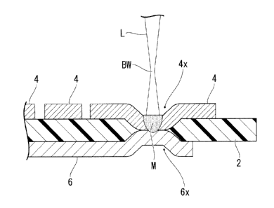
Next, as shown in FIG. 4A, laser beam L is made to strike the locations at
which
the depressions 4x and 6x are provided, so as to weld the antenna coil 4 and
the bridge
pattern 6. Although the laser beam L is shown as striking from the antenna
coil 4 side
in FIG. 4A, it can of course strike from the bridge pattern 6 side.
[0051]
In the case in which the forming material of a member to be welding is
aluminum, it is preferable that a YAG (yttrium aluminum garnet) laser having
an
oscillation wavelength of 1064 nm be used, and the in case of copper being the
forming
material, it is preferable that a YAG laser having an oscillation wavelength
of 532 nm be
used. The range of laser beam L energy is preferably from 1 J to 10 J.
[0052]
Using this type of laser beam L, for example, by distancing the focal point BW
from the surface of the antenna coil 4, the melted condition of the metal
material is
suppressed, and the antenna coil 4 and the bridge pattern 6 are welded. The
laser
conditions when this is done are such that the laser beam L is at a position
that is 5 mm
removed from the focal point BW as it strikes the surface of the antenna coil
4, with an
energy of 2.2 J.
[0053]
By doing this, as shown in FIG. 48 the antenna coil 4 and the bridge pattern 6
can be welded via the melted part M, without passing completely through the
antenna
coil 4 and the bridge pattern 6.
The foregoing manufactures the antenna sheet lA of the present embodiment.
[0054]
CA 02759688 2011-10-21
17
According to the antenna sheet 1A constituted as described above, the antenna
coil 4 and the bridge pattern 6, which are disposed on both sides of the
substrate 2, are
bonded together by melting. For this reason, the antenna coil 4 and the bridge
pattern 6
are physically strongly connected, and it is possible to use this as an
antenna sheet with
lowered electrical resistance and high stable electrical reliability.
[0055]
The object of lowering the resistance value between the antenna coil 4 and the
bridge pattern 6 is to eliminate the resistance value component at the contact
part between
the antenna coil 4 and the bridge pattern 6, so that there is only the
conductor resistance
of the metal that includes the welded part as well. By doing this, it is
possible to reduce
the instability element of an electrical connection made by only contacting
between the
antenna coil 4 and the bridge pattern 6, thereby achieving reliability.
If an electrical connection is made by only the contacting between the antenna
coil 4 and the bridge pattern 6, it is not possible to maintain the contact
resistance unless
a certain pressure is applied, and there is the possibility of oxidation or
corrosion of the
contact surfaces.
[0056]
According to the method of manufacturing the antenna sheet lA constituted as
noted above, it is possible to bond the antenna coil 4 and the bridge pattern
6 by
non-contact laser welding. For this reason, it is possible to achieve a
bonding condition
with stable quality, in contrast to the case of a contact-type process, in
which soiling or
wearing of a fixture influencing the bonding quality. Also, because there is
no fixture
replacement required, it is possible to achieve high production efficiency.
Because, by using laser welding, the resistance value component of the
connection part is eliminated, and there is the conductor resistance of the
metal that
includes the welded part as well, it is possible to reduce the instability
element of
connection, thereby achieving reliability.
[0057]
CA 02759688 2011-10-21
18
Although in the above-described manufacturing process, the description was for
the case in which the antenna coil 4 and the bridge pattern 6 in the antenna
sheet lA are
welded without passing through these two elements, the same type of process
can be used
to manufacture the antenna sheet 1 of a different embodiment. FIG. 5A and FIG.
5B are
process drawings for the method of manufacturing an antenna sheet 1B according
to
another embodiment of the present invention, these corresponding to FIG. 4A
and FIG.
4B.
[0058]
As shown in FIG. 5A, the focal point BW of the laser beam L is caused, for
example, to strike a position in the vicinity of the contact the surface of
the antenna coil 4
or the part of contact between the antenna coil 4 and the bridge pattern 6. By
doing this,
the laser beam L passes through the antenna coil 4 and the bridge pattern 6.
[0059]
For this reason, as shown in FIG. 5B, the periphery of the hole H that passes
through the antenna coil 4 and the bridge pattern 6 becomes the melted part M
and is
welded, so as to obtain the antenna sheet 1B, in which the antenna coil 4 and
the bridge
pattern 6 are welded. The diameter of the hole H is approximately 0.2 mm to 2
mm.
[0060]
In the antenna sheet 1B obtained in this manner, the material forming the
antenna coil 4 and the bridge pattern 6 are melted at the inner wall of the
hole H. By
doing this, the antenna coil 4 and the bridge pattern 6 are held together
strongly, enabling
the achievement of a highly reliable electrical connection.
[0061]
Also, when the antenna coil 4 and the bridge pattern 6 are welded by passing
the
laser beam L therethrough, because it is possible to check from the outer
appearance
whether or not the antenna coil 4 and the bridge pattern 6 are welded, it is
possible to
check for a poor connection.
[0062]
CA 02759688 2011-10-21
19
The IC inlet 10 according to the embodiment of the present invention is
preferably made by mounting the integrated circuit 20 as shown in FIG. lA and
FIG. 1B
after making an electrical connection between the antenna coil 4, the
connection terminal
5, and the bridge pattern 6, using the above-described method. In general, the
integrated
circuit 20 is more expensive than other members. For this reason, if the
antenna coil 4
and the bridge pattern 6 are connected after the integrated circuit 20 is
mounted, the loss
incurred by a failure occurring as a poor connection increases.
[0063]
(Data Recording Medium)
FIG. 6A and FIG. 6B describe a data recording medium 100 that has the
above-described IC inlet 10. FIG. 6A is a plan view of the data recording
medium 100,
and FIG. 6B is a cut-away cross-sectional view along the line B-B in FIG. 6A.
[0064]
As shown in FIG. 68, in the data recording medium 100, the IC inlet 10 is
sandwiched between protective members 110 and 120, and is bond in the
laminated
condition with the protective members 1 l 0 and 120.
[0065]
The material used for the protective members 110 and 120 may be, for example,
an insulating plastic film or an insulating synthetic paper (polyolefin
synthetic paper,
made by PPG under the product name of Teslin (registered trademark), or a
polypropylene-based synthetic paper made by Yupo Corporation under the product
name
YUPO (registered trademark)). The plastic film used for the material for
forming may
be a polyester resin such as PET-G (amorphous PET copolymer), or a
thermoplastic resin
such as PVC (polyvinyl chloride).
[0066]
In the case in which the protective members 110 and 120 are made of the
above-described plastic film, it is preferable to use a flexible plastic film.
Also, the
plastic film for forming is preferably one that has a softening temperature
that is lower
than that of the material for forming the base material of the IC inlet 10.
CA 02759688 2011-10-21
[0067]
The thickness of the protective members 110 and 120 can be, for example,
approximately 1001.1m to approximately 1000 jtm. It is preferable that the
thickness of
the protective members 110 and 120 be from approximately 100 i.tm to
approximately
500 'Am. By doing this, not only is it possible to achieve sufficient
functionality as a
base material, such as strength, but it is also possible to impart sufficient
flexibility to the
protective members 110 and 120, making application possible in booklet-type
applications.
[0068]
(Method for Manufacturing a Data Recording Medium)
Next, a method of manufacturing a data recording medium (inlay) 100 according
to the present embodiment will be described.
First, the IC inlet 10 is sandwiched between a pair of protective members 110
and 120, and the IC inlet 10 and the protective members 110 and 120 are bonded
together.
When this is done, an aperture somewhat larger than the outer shape of the
integrated
circuit may be formed in the protective members 110 which is in contact with
the
integrated circuit mounting surface of the IC inlet 10 at a position
corresponding to the
position of the integrated circuit 20 that is provided with the IC inlet 10
beforehand.
[0069]
In the case of using an above-described synthetic paper as the protective
members 110 and 120, the method of bonding the IC inlet 10 with the protective
members 110 and 120 is one of applying an adhesive to the antenna sheet 1 of
the IC inlet
10 or to the surfaces of the protective members 110 and 120 that make contact
with the
antenna sheet 1. Then, for example, an adhered laminate is made at a
relatively low
temperature of, for example, approximately 70 C to approximately 140 C.
[0070]
It is possible to use as the adhesive an EVA (ethylene vinyl acetate resin)
type,
an EAA (ethylene acrylate polymer resin), a polyester type, or a polyurethane
type or the
=
CA 02759688 2011-10-21
21
like. In place of the adhesive, an adhesive sheet using an adhesive as noted
above can
be sandwiched between the antenna sheet 1 and the protective members 110 and
120.
[0071]
In the case in which the above-noted thermoplastic film is used as the
protective
members 110 and 120, the method of bonding the IC inlet 10 and the protective
members
110 and 120 is that of heating both to a temperature that exceeds the
softening
temperature of the protective members 110 and 120 (for example, approximately
1300 to
approximately 170 ) while applying pressure to both. In the case of the
thermal
lamination method, the above-noted adhesive may be additionally used to assure
a
reliable melted bond.
[0072]
In the case of using plastic films as the protective members 110 and 120 as
described above, the softening temperature of the formation material is lower
than the
formation temperature of the formation material of the substrate 2. For this
reason, if
the protective members 110 and 120 and the IC inlet 10 are heated to
approximately 130
to approximately 170 , although the protective members 110 and 120 soften, the
substrate
2 of the antenna sheet 1 does not soften. The result is that, in the case in
which an IC
inlet 10 having an antenna sheet 1 is laminated and bonded by the thermal
lamination
method, even if heat is applied to the substrate 2 of the antenna sheet 1, the
substrate 2
does not plastically flow. It is therefore possible to prevent movement of the
antenna
coil 4 due to flowing of the substrate 2, and possible to improve the
reliability of data
communication.
[0073]
In the case in which the above-described lamination method is used for
attachment, and heating is done to above the softening temperature of the
substrate 2, so
that the substrate 2 becomes plastic and flows, the antenna coil 4, as
described above, is
band-shaped (film-shaped). For this reason, compared to a conventional winding
type
antenna coil, the contact surface between the antenna coil 4 and the substrate
2 is
increased, enabling the resistance of the antenna coil 4 to flowing to be
increased. It is
CA 02759688 2011-10-21
22
therefore possible to prevent movement of the antenna coil 4 accompanying the
flowing
of the substrate 2, thereby improving the reliability of data communication.
[0074]
If necessary in attachment by the lamination method, pressing is performed
from
one or both of the protective members 110 and 120, to securely bond the IC
inlet 10 and
to the protective films 110, and 120.
[0075]
After the bonding of the IC inlet 10 with the protective members 110 and 120,
processing is done to achieve the desired shape for the IC inlet 10 that is
integrated with
the protective members 110 and 120.
The foregoing manufactures the data recording medium 100 shown in FIG. 6A
and FIG. 6B.
[0076]
(Data Carrier with Non-Contact IC)
FIG. 7 is a drawing describing a booklet article that is one example of a data
carrier with a non-contact IC having the above-described data recording
medium. In
this case, an electronic passport will be taken as the example of the booklet
in the
description.
[0077]
As shown in FIG. 7 the electronic passport 200 has the above-described data
recording medium 100 as a cover. A cover material 201 that serves as the cover
of the
electronic passport 200 is bonding to the surface on one side of the data
recording
medium 100.
[0078]
By bonding the cover material 201 to the data recording medium 100 in this
manner, the look and feel of the electronic passport 200 having the data
recording
medium 100 can be made the same as a conventional passport. Also, the data
recording
medium 100 enables an electronic passport 200 that prevents open wires in the
antenna
coil, and also features superior manufacturability.
CA 02759688 2014-01-16
23
[0079]
The present invention is not restricted to the above-described embodiments.
For example, the shape of the antenna coil 4 need not be rectangular. Also,
the number
of turns in the antenna coil 4 is not restricted to the embodiments.
Additionally, although in the above-described embodiments an integrated
circuit
is shown as being disposed on the inside of the antenna coil, this is not a
restriction, and
disposition outside the antenna coil is also possible.
[0080]
Also, although in the above-described embodiments pressing is done by
sandwiching from both surfaces by two heat press heads (FIG. 3A and FIG. 3B),
one heat
press head 30 only may be used to perform heat pressing from only one
direction.
[0081]
Also, although in the above-described embodiments the description is for the
example of an electronic passport as a data carrier with a non-contact IC
having the data
recording medium 100, this is not a restriction, and use is also possible in,
for example,
electronic identification documents, and various documents that electronically
record and
verify a history of activities.
[0082]
Additionally, the data recording medium 100 according to the embodiment of
the present invention can also, for example, be applied to card-type data
carriers with a
non-contact IC, such as a commuter pass with an IC or an electronic money card
or the
like. By doing this, by the antenna sheet that has the IC inlet 10, it is
possible to prevent
open wires in a commuter pass with an IC or in an electronic money card,
thereby
improving reliability and also improving manufacturability.
CA 02759688 2014-01-16
24
various modifications are possible, based on design requirements or the like,
without
going beyond the scope of the spirit of the present invention.
[Examples]
[0083]
An example of the present invention is described below. In this example, in
order to verify the effect of the invention, the value of the resistance
between the antenna
coil 4 and the bridge pattern 6 in an antenna sheet 1 in which the connection
part was
laser-welded, as shown in the above-described FIG. 4B, was measured. As a
comparison example, the value of the resistance between the antenna coil 4 and
the
bridge pattern 6 in an antenna sheet 1 in which the connection part was only
in contact, as
shown in the above-described FIG. 3B, was measured. In the example of the
invention,
the resistance values of a plurality of test samples were measured and the
average thereof
taken.
[0084]
The results of the measurements were that, in the antenna sheet 1 of the
example
of the present invention in which the antenna coil 4 and the bridge pattern 6
were
laser-welded, the average resistance value was 15.6 mQ, In contrast, in the
antenna
sheet 1 in which the antenna coil 4 and the bridge pattern 6 were not laser-
welded but
were just in contact with one another, that is, in the antenna sheet 1 in
which the antenna
coil 4 and the bridge pattern 6 were brought into contact by crimping, the
average
resistance value was 18.6 ma
[0085]
From these results, it was verified that with the antenna sheet 1 having the
constitution of the embodiment of the present invention the electrical
resistance value
was decreased, and that the constitution of the embodiment of the present
invention had
the effect of solving the problem to be solved.
INDUSTRIAL APPLICABILITY
[0086]
CA 02759688 2014-01-16
The present invention can be applied to an antenna sheet that prevents open
wires in an antenna, improving the reliability and lowering the electrical
resistance, while
also improving the manufacturability.
Reference Symbols
[0087]
1, 1A, 1B Antenna sheet
2 Substrate
4 Antenna coil
4a, 4b Antenna coil ends
6 Bridge pattern, conductive member
8 Through hole
10 IC inlet
20 Integrated circuit (IC chip)
Heat press head (pressing unit)
110, 120 Protective member
100 Data recording medium
200 Electronic passport (data carrier with non-contact IC)
1-1 Hole
L Laser beam