Note: Descriptions are shown in the official language in which they were submitted.
1111;11-EFFICIENCY SOLAR CELL STRUCTURES AND
METHODS OF MANUFACTURE
Related Application Information
100011 This Application claims priority to U.S. Provisional Application
entitled "High-
Efficiency Solar Cell Structures and Methods of Manufacture." filed 21 April
2009 and assigned
application number 61/171,194.
Technical Field
100021 The present invention relates to solar cells. More particularly, the
present
invention relates to improved solar cell structures and methods of their
manufacture for increased
cell efficiency.
Rackaround of the Invention
100031 Solar cells are providing widespread benefits to society by
converting essentially
unlimited amounts of solar energy into useable electrical power. As their use
increases, certain
economic factors become important, such as high-volume manufacturing and
efficiency.
[00041 High volume manufacturing is generally considered to altain a high
degree of
cost-effectiveness and efficiency if the number of manufacturing steps. and
the complexity of
each step, can be minimized.
100051 Finished solar cell efficiencies of 20% or more are highly desired
in the industry,
however, known embodiments of such efficient cells often suffer from cell
structure complexity
and/or manufacturing complexity.
100061 What is required therefore. are solar cells which attain high
operational
efficiency, and which can be manufactured in a cost elTective manner.
-1-
2759708 2017-06-02
CA 02759708 2011-10-21
WO 2010/123974
PCT/US2010/031869
Summary of the Invention
[0007] The shortcomings of the prior art are overcome and additional
advantages are
provided by the present invention which in one aspect extends to any one or a
combination of
the solar cell structures disclosed below, including generally a central
substrate, conductive
layer(s), antireflection layers(s), passivation layer(s) and/or electrode(s).
Multifunctional
layers provide combined functions of passivation, transparency, sufficient
conductivity for
vertical carrier flow, the junction, and/or varying degrees of anti-
reflectivity. Improved
manufacturing methods including single-side CVD deposition processes and
thermal
treatment for layer formation and/or conversion are also disclosed.
[0008] In one aspect the present invention includes methods of fabricating
any of these
structures, including: providing a wafer as a central substrate; deposition or
growth of
interface passivation layers over the substrate; deposition of conductive
layers over the
passivation layers; providing thermal treatment; optional deposition of
antireflective layers
(possibly including back side mirrors); and providing metallization as
electrodes.
[0009] In one embodiment the present invention comprises applying a heat
treatment to
produce a multifunctional film which separates into a surface passivating
interface layer and
a highly doped polycrystalline passivation layer with high transparency.
[0010] In one embodiment the present invention comprises depositing an
amorphous,
silicon containing compound and using a heat treatment to initiate
crystallization into a
polycrystalline film.
[0011] In one embodiment the present invention comprises depositing an
amorphous,
silicon containing compound and using a heat treatment which leads to a
crystallization of the
film and increases the optical transmissivity.
[0012] In one embodiment the present invention comprises depositing an
amorphous,
silicon containing compound and using a heat treatment in order to activate
doping atoms in
the compound.
[0013] In one embodiment, the present invention comprises depositing an
amorphous,
silicon containing compound and using a thermal treatment greater than 500 C
in order to
activate doping atoms in the compound and result in diffusion of dopant atoms
into a
substrate wafer to provide a high-low junction or a p-n junction.
-2-
CA 02759708 2011-10-21
WO 2010/123974
PCT/US2010/031869
[0014] Systems and computer program products corresponding to the above-
summarized
methods are also described and claimed herein.
[0015] Further, additional features and advantages are realized through the
techniques of
the present invention. Other embodiments and aspects of the invention are
described in detail
herein and are considered a part of the claimed invention.
Brief Description of the Drawings
[0016] The subject matter which is regarded as the invention is
particularly pointed out
and distinctly claimed in the claims at the conclusion of the specification.
The foregoing and
other objects, features, and advantages of the invention are apparent from the
following
detailed description taken in conjunction with the accompanying drawings in
which:
[0017] Fig. 1 is an energy band diagram for an n-type crystalline
silicon solar cell with doped polysilicon layers and a passivated
interface;
[0018] Fig. 2 is a partial cross-sectional view of a solar cell
depicting
one type of minority and majority carrier flow for a front junction, p-
type wafer;
[0019] Fig. 3 is a partial cross-sectional view of a solar cell
depicting
one type of minority and majority carrier flow for a back junction, p-
type wafer;
[0020] Fig. 4 is a partial cross-sectional view of a solar cell
depicting
one type of minority and majority carrier flow for a front junction, n-
type wafer;
[0021] Fig. 5 is a partial cross-sectional view of a solar cell
depicting
one type of minority and majority carrier flow for a back junction, n-
type wafer;
[0022] Fig. 6 is a partial cross-sectional view of a solar cell having n-
type front, n- or p-type wafer, and p-type back;
-3-
CA 02759708 2011-10-21
WO 2010/123974
PCT/US2010/031869
[0023] Fig. 7 is a partial cross-sectional view of a solar cell having n-
type front, n- or p-type wafer, p-type back, in a bifacial configuration;
[0024] Fig. 8 is a partial cross-sectional view of a solar cell having n-
type front, n-type wafer, p-type back, and includes isolating the
antireflection coating;
[0025] Fig. 9 is a partial cross-sectional view of a solar cell having n-
type front, n-type wafer, p-type back, and includes a multifunctional
transparent, conductive, highly doped silicon compound layer;
[0026] Fig. 10 is a partial cross-sectional view of a solar cell having n-
or p-type wafer, n-type front, including certain front layer
improvements, and p-type back;
[0027] Fig. 11 is a partial cross-sectional view of a solar cell having a
p-type front, n- or p-type wafer, and n-type back;
[0028] Fig. 12 is a partial cross-sectional view of a solar cell having p-
type front, n- or p-type wafer, n-type back, in a bifacial configuration;
[0029] Fig. 13 is a partial cross-sectional view of a solar cell having p-
type front, p-type wafer, n-type back, and includes isolating the
antireflection coating;
[0030] Fig. 14 is a partial cross-sectional view of a solar cell having p-
type front, p-type wafer, n-type back, and including a multifunctional
transparent, conductive, highly doped silicon compound layer;
[0031] Fig. 15 is a partial cross-sectional view of a solar cell having n-
or p-type wafer, p-type front, including certain front layer
improvements, and n-type back;
[0032] Fig. 16 is a partial cross-sectional view of a solar cell having
glass or other transparent film with embedded electrodes, compressed
or bonded to the cell;
-4-
CA 02759708 2011-10-21
WO 2010/123974
PCT/US2010/031869
[0033] Fig. 17 is a partial cross-sectional view of a solar cell having
glass or other transparent film with embedded electrodes, compressed
or bonded to the cell, including a localized electrode on the back; and
[0034] Fig. 18 is a partial cross-sectional view of a solar cell having
additional silicon buffer layers formed therein;
[0035] all in accordance with the present invention.
Description of the Invention
[0036] With reference to the energy band diagram and partial cross-
sectional views of
exemplary solar cells of Figs. 1-5, solar radiation is assumed to
preferentially illuminate one
surface of a solar cell, usually referred to as the front side. To achieve
high energy
conversion efficiency of incident photons into electric energy, an efficient
absorption of
photons within the silicon substrate material forming the cell is important.
This can be
achieved by a low parasitic optical absorption of photons within all layers
except the
substrate itself.
[0037] For the sake of simplicity, the geometrical surface shape of layer
surfaces (e.g.,
surface texture such as pyramids, or other surface texture, can be formed on
layer surfaces) is
not portrayed in these drawings, however, it is understood that the
geometrical shape and/or
surfaces may be textured in any shape beneficial for improved solar cell
efficiency, and falls
within the scope of the invention.
[0038] One important parameter for high solar cell efficiency is surface
passivation.
Surface passivation provides suppression of recombination of electrons and
holes at or in the
vicinity of certain physical surfaces within the solar cell. Surface
recombination can be
reduced by the application of dielectric layers. These layers reduce the
interface density of
states and therefore reduce the number of recombination centers. Two examples
are
thermally grown silicon oxide and PECVD deposited silicon nitride. Another
example of a
surface passivating layer is intrinsic amorphous silicon. These layers can
also provide an
electrical charge which reduces the number of carriers of the opposite
polarity and reduces
recombination rates via this mechanism. Two examples are silicon nitride and
aluminum
oxide.
-5-
CA 02759708 2011-10-21
WO 2010/123974
PCT/US2010/031869
[0039] Another method of reducing the amount of carriers of one type close
to a surface
is the diffusion of doping atoms either of the same or the opposite doping of
the layer doping
type. In this case doping levels in excess of the layer doping are necessary
to obtain a high-
low junction (also commonly called back surface field or front surface field)
or a p-n
junction. This can be combined with other methods of surface passivation
mentioned above.
[0040] Surface passivation can play an important role in achieving highly
efficient solar
cells. In most of the solar cell structures described below in accordance with
the present
invention, multiple layers or multifunctional layers can provide excellent
surface passivation.
This can be achieved via a very steep doping profile and an additional
passivation of the
interface using a layer with low interface state density and a high band gap
resulting in a
tunneling barrier for substrate minority carriers to pass. A corresponding
energy band
diagram is shown in Fig. 1. The solid lines depict the case of an n-type
crystalline silicon
wafer with a passivated interface and doped polycrystalline silicon
passivation layers. The
dotted lines represent the case of an n-type crystalline silicon wafer and a
double layer
structure of intrinsic amorphous silicon followed by doped amorphous silicon
layer,
sometimes referred to as a heterojunction cell.
[0041] These structures provide another benefit for a highly efficient
solar cell: the
recombination in areas underneath the contacts can be as low as in areas
without contacts.
The contacts can be shielded by the passivation. As a result, the contact area
can be
optimized for optical properties, thus minimizing resistive losses, but
carrier recombination is
decoupled.
[0042] Depending on the choice of materials, and doping types and
concentrations, the
disclosed cell structures may be categorized as front-junction or back-
junction cells. In a
front-junction cell the minority carriers (in the case of a p-type wafer these
are electrons) are
collected on the side of illumination. In a back junction cell the minority
carriers are
collected at the side opposed to the illumination. Current flow patterns are
shown generally
in the partial cross-sectional solar cell views of Figs. 2-5 for p-type and n-
type wafers.
[0043] Fig. 2 shows carrier flow for a solar cell 20, in which minority
carriers (solid
lines) flow to front electrodes 21 from a p-type wafer 25 having a front
junction. The
electrons need to use lateral flow within the thin n-type emitter 22 to reach
the electrodes 21,
-6-
CA 02759708 2011-10-21
WO 2010/123974
PCT/US2010/031869
and the lateral sheet resistance of the emitter 22 increases resistive losses.
The majority
carriers (dashed lines) can use the shortest geometrical path to the full area
back electrode 29.
[0044] Fig. 3 shows carrier flow for a solar cell 30 from p-type wafer 35
having a back
junction. The majority carriers (dashed lines) can use the entire wafer
conductivity to reach
the front electrodes 31. The minority carriers (solid lines) can use the
shortest geometrical
path to reach the rear n-type emitter 38, and their transport within the
emitter is vertical
instead of mainly lateral. This back junction structure reduces the
requirements for lateral
conductivity of the emitter layer.
[0045] Fig. 4 shows carrier flow for a solar cell 40, in which minority
carriers (solid
lines) flow to front electrodes 41 from an n-type wafer 45 having a front
junction. The holes
need to use lateral flow within the thin p-type emitter 42 to reach the
electrodes 41, and the
lateral conductivity of the emitter determines the resistive losses. The
majority carriers
(dashed lines) can use the shortest geometrical path to the full area back
electrode 49.
[0046] Fig. 5 shows carrier flow for a solar cell 50 from an n-type wafer
55 having a back
junction. The majority carriers (dashed lines) can use the entire wafer
conductivity to reach
the front electrodes 51. The minority carriers (solid lines) can use the
shortest geometrical
path to reach the rear p-type emitter 58, and their transport within the
emitter is vertical
instead of mainly lateral. This back junction structure reduces the
requirements for lateral
conductivity of the emitter layer.
[0047] A back junction cell with a full area back contact has the advantage
that the
minority carriers do not have to flow laterally through the emitter to reach
the contacts, their
transport within the emitter is mainly vertical. This reduces the losses
associated with the
lateral transport of the minority carriers within the emitter. Since the full
contact area
coverage is a requirement to benefit from this property of the structure, a
shielded contact is
important, e.g., since the metal contacts the layer everywhere ("full area
contact coverage"),
there is no need for the minority carriers to flow laterally toward the
nearest contact, like they
do within the emitter in, e.g., Fig. 4.
Exemplary Cell Structures: n-type front, n- or p-type wafer, p-type back:
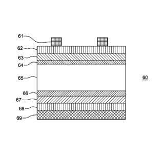
[0048] Fig. 6 is a partial cross-sectional view of a solar cell 60 having
an n-type front, n-
or p-type wafer, and p-type back.
-7-
CA 02759708 2011-10-21
WO 2010/123974
PCT/US2010/031869
[0049] The metal electrodes 61 and 69 are positioned on the outer layers 62
and 68,
respectively. This has the benefit that the metal does not need to penetrate
underlying layers
before it contacts the wafer. Furthermore the silicon bulk wafer 65 is
shielded from the
contact interfaces and hence the contact interface carrier recombination is
minimized. This
structure has an n-type front surface, which for a p-type wafer 65 collects
the minority
carriers (electrons) on the front. Therefore a maximum lateral sheet
resistance of, for
example, 500 Ohm/sq of the combined layers 62, 63 and 64 is required. For an n-
type wafer
this structure collects the minority carriers (holes) on the back. Therefore
the current flow
pattern in the solar cell is different and the requirements of lateral
conductivity of layer 62 are
less critical. Exemplary layers of cell 60 include the following:
[0050] 61: Front metal electrode.
[0051] 62: Transparent and conductive film, refractive index in the range
of 1.4 < n < 3;
thickness in the range of 20 nm <thickness<110 nm; sheet resistance of less
than 500 Ohm/sq
for a p-type wafer (front junction solar cell), specific resistivity in the
range of rho < 1000
Ohm cm for an n-type wafer (back junction solar cell). Examples include
transparent
conductive oxides like indium tin oxide, aluminum doped zinc oxide, fluorine
doped tin
oxide, tantalum oxide, antimony tin oxide, germanium oxide, zirconium oxide,
titanium
oxide, gallium oxide, cadmium antimony oxide.
[0052] 63: Electrically passivating and conductive film, highly n-doped le
18 cm-3< ND
<5e21 cm-3 ; thickness in the range of 2 nm <thickness<50 nm; specific
resistivity in the
range of rho < 1000 Ohm cm. Examples include:
= n-type amorphous or polycrystalline silicon carbides: phosphorus
doped silicon carbide, nitrogen doped silicon carbide;
= n-type amorphous or polycrystalline silicon: phosphorus doped
amorphous silicon, nitrogen doped amorphous silicon;
= n-type amorphous or poly-crystalline diamond-like-carbon: nitrogen
doped diamond-like carbon.
[0053] Any of the above listed examples may include oxygen and hydrogen (n-
doped
SiCx0yHz; n-doped SiNx0yHz).
-8-
CA 02759708 2011-10-21
WO 2010/123974
PCT/US2010/031869
[0054] 64: Electrically passivating interface layer; thickness <10 nm; no
conductivity
requirements because of small thickness; no absorption restrictions due to
small thickness.
Examples include silicon oxide, silicon nitride, intrinsic amorphous silicon,
intrinsic
polycrystalline silicon, aluminum oxide, aluminum nitride, phosphorus nitride,
titanium
nitride.
[0055] 65: n-type or p-type crystalline silicon wafer; thickness is the
range of w<300 urn,
base resistivity for n-type wafers 0.5 Ohm cm < rho < 20 Ohm cm, for p-type
wafers 0.1
Ohm cm < rho < 100 Ohm cm.
[0056] 66: Electrically passivating interface layer; thickness <10 nm; no
conductivity
requirements because of small thickness; no absorption restrictions due to
small thickness.
Examples include silicon oxide, silicon nitride, intrinsic amorphous silicon,
intrinsic
polycrystalline silicon, aluminum oxide, aluminum nitride, phosphorus nitride,
titanium
nitride.
[0057] 67: Electrically passivating and conductive film, highly p-doped
1E18-5E21/cm3;
specific resistivity in the range of rho < 1000 Ohm cm. Examples include:
= p-type amorphous or polycrystalline silicon carbides: boron doped
silicon carbide, aluminum doped silicon carbide, gallium doped silicon
carbide;
= p-type amorphous or polycrystalline silicon: boron doped silicon,
aluminum doped silicon, gallium doped silicon;
= p-type amorphous or poly-cystalline diamond-like-carbon: boron
doped diamond-like carbon, aluminum doped diamond-like carbon.
[0058] Any of the above examples may include oxygen and hydrogen (p-doped
SiCx0yHL; p-doped SiNx0y1-1,).
[0059] 68: transparent and conductive film, refractive index in the range
of 1.4 < n < 3;
specific resistivity in the range of rho < 1000 Ohm cm. Examples include
conductive oxides
like indium tin oxide, aluminum doped zinc oxide, fluorine doped tin oxide,
tantalum oxide,
antimony tin oxide, germanium oxide, zirconium oxide, titanium oxide, gallium
oxide,
cadmium antimony oxide.
-9-
CA 02759708 2011-10-21
WO 2010/123974
PCT/US2010/031869
[0060] 69: back metal electrode.
[0061] Fig. 7 is a partial cross-sectional view of a solar cell 70 having n-
type front, n- or
p-type wafer, p-type back, in a bifacial configuration. Cell 70 is similar to
cell 60 but
includes localized electrodes 79 on the back. Because of the localized
structure on the back,
photons impinging from the rear of the solar cell can be absorbed within the
wafer 75 and
produce electron-hole pairs. This can increase the power output generated by
the solar cell
under outdoor operating conditions where albedo can be used at low additional
module
manufacturing and installation cost.
[0062] Fig. 8 is a partial cross-sectional view of a solar cell 80 having n-
type front, n-type
wafer, p-type back, and includes isolating the antireflection coating. This
structure is
especially beneficial for material combinations where the conductive layers on
the front
surface of cell structures 60 and 70 have a high absorption. By placing the
electrode 81
directly on the contacting layer 83 the conductivity requirements of layer 82
are waived and
traditional antireflection coating films (which are insulators) can be used.
Exemplary layers
of cell 80 include the following:
[0063] 81: Front metal electrode.
[0064] 82: Antireflection film, refractive index in the range of 1.4 <n <
3; thickness in
the range of 20 nm <thickness<110 nm. Examples include silicon nitride,
silicon carbide,
silicon oxide, transparent conductive oxides.
[0065] 83: Electrically passivating and conductive film; thickness <110 nm
; highly n-
doped 1e18 cm-3<ND<5e21 cm-3, specific resistivity in the range of rho < 1000
Ohm cm.
Examples include:
= n-type amorphous or polycrystalline silicon carbides: phosphorus
doped silicon carbide, nitrogen doped silicon carbide;
= n-type amorphous or polycrystalline silicon: phosphorus doped
amorphous silicon, nitrogen doped amorphous silicon;
= n-type amorphous or poly-crystalline diamond-like-carbon: nitrogen
doped diamond-like carbon.
-10-
CA 02759708 2011-10-21
WO 2010/123974
PCT/US2010/031869
[0066] Any of the above examples may include oxygen and hydrogen (n-doped
SiCx0yHz; n-doped Sil\Tx0yHz).
[0067] 84: Electrically passivating interface layer; thickness thickness<10
nm ; no
conductivity requirements because of small thickness; no absorption
restrictions due to small
thickness. Examples include silicon oxide, silicon nitride, intrinsic
amorphous silicon,
intrinsic polycrystalline silicon, aluminum oxide, aluminum nitride,
phosphorus nitride,
titanium nitride.
[0068] 85: n-type crystalline silicon wafer; thickness is in the range of
w<300 urn, base
resistivity for n-type wafers 0.5 Ohm cm < rho < 20 Ohm cm.
[0069] 86: Electrically passivating interface layer; thickness<10 nm; no
conductivity
requirements because of small thickness; no absorption restrictions due to
small thickness.
Examples include silicon oxide, silicon nitride, intrinsic amorphous silicon,
intrinsic
polycrystalline silicon, aluminum oxide, aluminum nitride, phosphorus nitride,
titanium
nitride.
[0070] 87: Electrically passivating and conductive film, highly doped p-
doped 1e18 cm-
3<NA<5 e2 1 cm 3; specific resistivity in the range of rho < 1000 Ohm cm.
Examples include:
= p-type amorphous or polycrystalline silicon carbides: boron doped
silicon carbide, aluminum doped silicon carbide, gallium doped silicon
carbide;
= p-type amorphous or polycrystalline silicon: boron doped silicon,
aluminum doped silicon, gallium doped silicon;
= p-type amorphous or poly-cystalline diamond-like-carbon: boron
doped diamond-like carbon, aluminum doped diamond-like carbon.
[0071] Any of the above examples may contain oxygen and hydrogen (p-doped
SiCx0yHz; p-doped SiNx0y1-10.
[0072] 88: Transparent and conductive film, refractive index in the range
of 1.4 < n < 3;
specific resistivity in the range of rho < 1000 Ohm cm. Examples include
transparent
conductive oxides like indium tin oxide, aluminum doped zinc oxide, fluorine
doped tin
-11-
CA 02759708 2011-10-21
WO 2010/123974
PCT/US2010/031869
oxide, tantalum oxide, antimony tin oxide, germanium oxide, zirconium oxide,
titanium
oxide, gallium oxide, cadmium antimony oxide.
[0073] 89: back metal electrode.
[0074] Fig. 9 is a partial cross-sectional view of a solar cell 90 having n-
type front, n-type
wafer, p-type back, and including a multifunctional transparent, conductive,
highly doped
silicon compound layer. This aspect of the invention is an improvement to the
other
disclosures above, because the functions of layers 62 and 63 of, e.g., solar
cell 60 of Fig. 6
(and any other similar layers in any other embodiments disclosed herein) are
combined into a
multifunctional layer 93a depicted in Fig. 9. This layer can be electrically
passivating,
transparent, and sufficiently conductive for a vertical carrier flow to the
electrodes (back
junction solar cell), provides the junction with the wafer 95 and/or reduces
the reflectance of
the incoming light (e.g., antireflection coating). On the rear, layer 97a can
combine the
functions of layers 67 and 68 of, e.g., solar cell 60 of Fig. 6 (and any other
similar layers in
any other embodiments disclosed herein). Layer 97a provides the junction with
the wafer 95,
has a refractive index which results in a high reflectivity for photons of
more than 900 nm
wavelength and is sufficiently conductive for vertical carrier flow from the
wafer 95 to the
metal electrode 99. Exemplary layers of cell 90 include the following:
[0075] 91: Front metal electrode.
[0076] 93a: Electrically passivating, transparent and conductive film,
refractive index in
the range of 1.4 < n < 3; thickness in the range of 20 nm <thickness<110 nm;
specific
resistivity in the range of rho < 1000 Ohm cm for an n-type wafer; highly
doped n-doped
1e18 cm-3<ND<5e21 cm-3.. Examples include:
= n-type amorphous or polycrystalline silicon carbides: phosphorus
doped silicon carbide, nitrogen doped silicon carbide;
= n-type amorphous or polycrystalline silicon: phosphorus doped
amorphous silicon, nitrogen doped amorphous silicon;
= n-type amorphous or poly-crystalline diamond-like-carbon: nitrogen
doped diamond-like carbon.
-12-
CA 02759708 2011-10-21
WO 2010/123974
PCT/US2010/031869
[0077] Any of the above examples may include oxygen and hydrogen (n-doped
SiCx0y1-1,; n-doped SiNx0yHz).
[0078] 94: Electrically passivating interface layer; thickness <10 nm; no
conductivity
requirements because of small thickness; no absorption restrictions due to
small thickness.
Examples include silicon oxide, silicon nitride, intrinsic amorphous silicon,
intrinsic
polycrystalline silicon, aluminum oxide, aluminum nitride, phosphorus nitride,
titanium
nitride.
[0079] 95: n-type or p-type crystalline silicon wafer; thickness is in the
range of w<300
um, base resistivity for n-type wafers 0.5 Ohm cm < rho <20 Ohm cm, for p-type
wafers 0.1
Ohm cm < rho < 100 Ohm cm.
[0080] 96: Electrically passivating interface layer; thickness <10 nm ; no
conductivity
requirements because of small thickness; no absorption restrictions due to
small thickness.
Examples include silicon oxide, silicon nitride, intrinsic amorphous silicon,
intrinsic
polycrystalline silicon, aluminum oxide, aluminum nitride, phosphorus nitride,
titanium
nitride.
[0081] 97a: Electrically passivating and transparent and conductive film;
specific
resistivity in the range of rho < 1000 Ohm cm. Examples include:
= p-type amorphous or polycrystalline silicon carbides: boron doped
silicon carbide, aluminum doped silicon carbide, gallium doped silicon
carbide;
= p-type amorphous or polycrystalline silicon: boron doped silicon,
aluminum doped silicon, gallium doped silicon;
= p-type amorphous or poly-crystalline diamond-like-carbon: boron
doped diamond-like carbon, aluminum doped diamond-like carbon.
[0082] Any of the above examples may include oxygen and hydrogen (p-doped
SiCx0"; p-doped SiNx0yEtz).
[0083] 99: back metal electrode.
-13-
CA 02759708 2011-10-21
WO 2010/123974
PCT/US2010/031869
[0084] Fig. 10 is a partial cross-sectional view of a solar cell 100 having
n- or p-type
wafer, n-type front, including certain front layer improvements, and p-type
back. The rear
surface structures (omitted for convenience) can be implemented according to
any of the
other structures described herein.
[0085] This structure is especially beneficial for material combinations
where the layers
x3 and x4 on, e.g., the front surface of structures disclosed above, have
unacceptably high
absorption. (The x3 and x4 notation is further explained below and represents
any of the
above layers with reference numerals ending in 3,3a, 4, 4a, respectively). In
cell 100, by
placing layers 103 and 104 under the contacts only, their optical properties
(refractive index,
absorption) arc not important for cell efficiency. Resistance losses only
occur through
vertical carrier flow to the contacts 101. Layers 102, 104b and 105b also do
not have to
shield the contact, so they can be optimized for transmissivity and surface
passivation. If
they do provide lateral conductivity, this will facilitate the current flow
towards the contacts
and the contact structures can be placed further apart from each other. This
reduces optical
shading losses. This structure works best with a back junction since the
lateral conductivity
requirements of layer 102, 104b and 105b are waived. Exemplary layers of cell
100 include
the following:
[0086] 101: Front metal electrode.
[0087] 102: Antireflection film, refractive index in the range of 1.4 < n <
3; thickness
<150 nm. Examples include silicon nitride, silicon carbide, silicon oxide,
titanium oxide,
transparent conductive oxides.
[0088] 103: Electrically passivating conductive film, e.g., thickness <50
nm ; e.g.,
specific resistivity in the range of rho < 1000 Ohm cm. Examples include:
= n-type amorphous or polycrystalline silicon carbides: phosphorus
doped silicon carbide, nitrogen doped silicon carbide;
= n-type amorphous or polycrystalline silicon: phosphorus doped
amorphous silicon, nitrogen doped amorphous silicon;
= n-type amorphous or poly-crystalline diamond-like-carbon: nitrogen
doped diamond-like carbon.
-14-
CA 02759708 2011-10-21
WO 2010/123974
PCT/US2010/031869
[0089] Any of the above examples may include oxygen and hydrogen (n-doped
SiCx0yI-1,; n-doped SiNx0yHz).
[0090] 104: Electrically passivating interface layer; thickness <10 nm ; no
conductivity
requirements because of small thickness; no absorption restrictions due to
small thickness.
Examples include silicon oxide, silicon nitride, intrinsic amorphous silicon,
intrinsic
polycrystalline silicon, aluminum oxide, aluminum nitride, phosphorus nitride,
titanium
nitride.
[0091] 104b: Electrically passivating interface layer; thickness <110 nm.
Examples
include silicon oxide, silicon nitride, intrinsic amorphous silicon, intrinsic
polycrystalline
silicon, aluminum oxide, aluminum nitride, phosphorus nitride, titanium
nitride, silicon
carbide or stacks of two or more of these materials.
[0092] 105: n-type or p-type crystalline silicon wafer; thickness is in the
range of w<300
um, base resistivity for n-type wafers 0.5 Ohm cm < rho <20 Ohm cm, for p-type
wafers 0.1
Ohm cm < rho < 100 Ohm cm.
[0093] 105b: phosphorus diffused silicon layer (optional), sheet resistance
>70 Ohm/sq.
[0094] The structures above are not mutually exclusive, and any feature of
one structure,
can apply to any other structure herein, in accordance with the present
invention.
Exemplary Cell Structures: p-type front, n- or p-type wafer, n-type back:
[0095] Fig. 11 is a partial cross-sectional view of a solar cell 110 having
a p-type front, n-
or p-type wafer, and n-type back.
[0096] In this cell, the metal electrodes 111and 119 are placed on the
outer layers 112 and
118, respectively. This provides the benefit that the metal does not need to
penetrate
underlying layers before it contacts the wafer. Furthermore the silicon bulk
wafer 115 is
shielded from the contact interfaces and hence the contact interface carrier
recombination is
minimized. This structure has a p-type front surface, for an n-type wafer this
structure
collects the minority carriers (holes) on the front. Therefore a maximum
lateral sheet
resistance of 500 Ohm/sq of the combined layers 112, 113 and 114 is allowed.
For a p-type
wafer this structure collects the minority carriers (electrons) on the back.
Therefore the
-15-
CA 02759708 2011-10-21
WO 2010/123974
PCT/US2010/031869
current flow pattern in the solar cell is different and the requirements on
the lateral
conductivity of layer 112 are less critical. Exemplary layers of cell 110
include the
following:
[0097] 111: Front metal electrodes.
[0098] 112: Transparent and conductive film, refractive index in the range
of 1.4 < n < 3;
thickness<110 nm ; sheet resistance of less than 500 Ohmisq for an n-type
wafer, specific
resistivity in the range of rho < 1000 Ohm cm for a p-type wafer. Examples
include
transparent conductive oxides like indium tin oxide, aluminum doped zinc
oxide, fluorine
doped tin oxide, tantalum oxide, antimony tin oxide, germanium oxide,
zirconium oxide,
titanium oxide, gallium oxide, cadmium antimony oxide.
[0099] 113: Electrically passivating and conductive film, highly doped p-
doped lel 8 cm-
3<NA<5 e2 1 cm-3; specific resistivity in the range of rho < 1000 Ohm cm.
Examples include:
= p-type amorphous or polycrystalline silicon carbides: boron doped
silicon carbide, aluminum doped silicon carbide, gallium doped silicon
carbide;
= p-type amorphous or polycrystalline silicon: boron doped silicon,
aluminum doped silicon, gallium doped silicon;
= p-type amorphous or poly-crystalline diamond-like-carbon: boron
doped diamond-like carbon, aluminum doped diamond-like carbon.
[00100] Any of the above examples may include oxygen and hydrogen (p-doped
SiCx0yHz; p-doped SiNx0yHz).
[00101] 114: Electrically passivating interface layer; <10 nm; no
conductivity
requirements because of small thickness; no absorption restrictions due to
small thickness.
Examples include silicon oxide, silicon nitride, intrinsic amorphous silicon,
intrinsic
polycrystalline silicon, aluminum oxide, aluminum nitride, phosphorus nitride,
titanium
nitride.
-16-
CA 02759708 2011-10-21
WO 2010/123974
PCT/US2010/031869
[00102] 115: n-type or p-type crystalline silicon wafer; thickness is in
the range of w<300
um, base resistivity for n-type wafers 0.5 Ohm cm < rho <20 Ohm cm, for p-type
wafers 0.1
Ohm cm < rho < 100 Ohm cm.
[00103] 116: Electrically passivating interface layer; thickness <10 nm ;
no conductivity
requirements because of small thickness; no absorption restrictions due to
small thickness.
Examples include silicon oxide, silicon nitride, intrinsic amorphous silicon,
intrinsic
polycrystalline silicon, aluminum oxide, aluminum nitride, phosphorus nitride,
titanium
nitride.
[00104] 117: Electrically passivating, transparent and conductive film,
highly doped n-
doped 1e18 cm-3<ND<5e21 cm-3; e.g., thickness in the range of 2 nm
<thickness<50 nm or
more; specific resistivity in the range of rho < 1000 Ohm cm. Examples
include:
= n-type amorphous or polycrystalline silicon carbides: phosphorus
doped silicon carbide, nitrogen doped silicon carbide;
= n-type amorphous or polycrystalline silicon: phosphorus doped
amorphous silicon, nitrogen doped amorphous silicon;
= n-type amorphous or poly-crystalline diamond-like-carbon: nitrogen
doped diamond-like carbon.
[00105] Any of the above examples may contain oxygen and hydrogen (n-doped
SiCx0y1-1,; n-doped SiNx0yHz).
[00106] 118: Transparent and conductive film, refractive index in the range
of 1.4 < n < 3;
specific resistivity in the range of rho < 1000 Ohm cm. Examples include
transparent
conductive oxides like indium tin oxide, aluminum doped zinc oxide, fluorine
doped tin
oxide, tantalum oxide, antimony tin oxide, germanium oxide, zirconium oxide,
titanium
oxide, gallium oxide, cadmium antimony oxide.
[00107] 119: back metal electrode.
[00108] Fig. 12 is a partial cross-sectional view of a solar cell 120
having p-type front, n-
or p-type wafer, n-type back, in a bifacial configuration. Cell 120 is similar
to cell 110 but
includes localized electrodes 129 on the back. Because of the localized
structure on the back,
-17-
CA 02759708 2011-10-21
WO 2010/123974
PCT/US2010/031869
photons impinging from the rear of the solar cell can be absorbed within the
wafer 125 and
produce electron-hole pairs. This can improve the efficiency of the solar cell
under outdoor
operating conditions where albedo can be used at low additional module
manufacturing and
installation cost.
[00109] Fig. 13 is a partial cross-sectional view of a solar cell 130
having p-type front, p-
type wafer, n-type back, and includes isolating the antireflection coating.
This structure is
especially beneficial for material combinations where the conductive layers on
the front
surface of cell structures 110 and 120 have a high absorption. By placing the
electrodes 131
directly on the contacting layer 133 the conductivity requirements of layer
132 are waived
and traditional antireflection coating films (which are insulators) can be
used. This structure
works best with a back junction since the lateral conductivity requirements of
layer 133 and
134 are not critical. Exemplary layers of cell 130 include the following:
[00110] 131: Front metal electrodes.
[00111] 132: Antireflection film, refractive index in the range of 1.4 <n <
3; <150 nm.
Examples include silicon nitride, silicon carbide, silicon oxide, aluminum
oxide, titanium
oxide, transparent conductive oxides.
[00112] 133: Electrically passivating, transparent and conductive film;
thickness <110 nm;
specific resistivity in the range of rho < 1000 Ohm cm. Examples include:
= p-type amorphous or polycrystalline silicon carbides: boron doped
silicon carbide, aluminum doped silicon carbide, gallium doped silicon
carbide;
= p-type amorphous or polycrystalline silicon: boron doped silicon,
aluminum doped silicon, gallium doped silicon;
= p-type amorphous or poly-cystalline diamond-like-carbon: boron
doped diamond-like carbon, aluminum doped diamond-like carbon.
[00113] Any of the above examples may include oxygen and hydrogen (p-doped
SiCx0yHz; p-doped SiNx0yHz).
-18-
CA 02759708 2011-10-21
WO 2010/123974
PCT/US2010/031869
[00114] 134: Electrically passivating interface layer; thickness <10 nm; no
conductivity
requirements because of small thickness; no absorption restrictions due to
small thickness.
Examples include silicon oxide, silicon nitride, intrinsic amorphous silicon,
intrinsic
polycrystalline silicon, aluminum oxide, aluminum nitride, phosphorus nitride,
titanium
nitride.
[00115] 135: p-type crystalline silicon wafer; thickness is the range of
w<300 um, base
resistivity for p-type wafers 0.1 Ohm cm < rho < 100 Ohm cm.
[00116] 136: Electrically passivating interface layer; thickness <10 nm; no
conductivity
requirements because of small thickness; no absorption restrictions due to
small thickness.
Examples include silicon oxide, silicon nitride, intrinsic amorphous silicon,
intrinsic
polycrystalline silicon, aluminum oxide, aluminum nitride, phosphorus nitride,
titanium
nitride.
[00117] 137: Electrically passivating, transparent and conductive film,
highly doped n-
doped 1e18 cm-3<ND<5e21 cm3 ; specific resistivity in the range of rho < 1000
Ohm cm.
Examples include:
= n-type amorphous or polycrystalline silicon carbides: phosphorus
doped silicon carbide, nitrogen doped silicon carbide;
= n-type amorphous or polycrystalline silicon: phosphorus doped
amorphous silicon, nitrogen doped amorphous silicon;
= n-type amorphous or poly-crystalline diamond-like-carbon: nitrogen
doped diamond-like carbon.
[00118] Any of the above examples may include oxygen and hydrogen (n-doped
SiCx0y1-17; n-doped SiNx0yH7).
[00119] 138: transparent and conductive film, refractive index in the range
of 1.4 <n < 3;
specific resistivity in the range of rho < 1000 Ohm cm. Examples include
transparent
conductive oxides like indium tin oxide, aluminum doped zinc oxide, fluorine
doped tin
oxide, tantalum oxide, antimony tin oxide, germanium oxide, zirconium oxide,
titanium
oxide, gallium oxide, cadmium antimony oxide.
-19-
CA 02759708 2011-10-21
WO 2010/123974
PCT/US2010/031869
[00120] 139: back metal electrode.
[00121] Fig. 14 is a partial cross-sectional view of a solar cell 140
having p-type front, p-
type wafer, n-type back, and including a multifunctional transparent,
conductive, highly
doped silicon compound layer. This aspect of the invention is an improvement
to the other
disclosures above, because the functions of layers 112 and 113 of, e.g., solar
cell 110 of Fig.
11 (and any other similar layers in any other embodiments disclosed herein)
are combined
into a multifunctional layer 143a depicted in Fig. 14. This layer can be
electrically
passivating, transparent, and sufficiently conductive for a vertical carrier
flow to the
electrodes (back junction solar cell), provides the junction with the wafer
145 and/or reduces
the reflectance of the incoming light (e.g., antircflection coating). On the
rear, layer 147a can
combine the functions of layers 117 and 118 of, e.g., solar cell 110 of Fig.
11 (and any other
similar layers in any other embodiments disclosed herein). Layer 147a provides
the junction
with the wafer 145, has a refractive index which results in a high
reflectivity for photons of
more than 900 nm wavelength and is sufficiently conductive for vertical
carrier flow from the
wafer 145 to the metal electrode 149. Exemplary layers of cell 140 include the
following:
[00122] 141: Front metal electrode.
[00123] 143a: Electrically passivating and transparent and conductive film,
refractive
index in the range of 1.4 <n < 3; thickness <150 nm ; specific resistivity in
the range of rho <
1000 Ohm cm. Examples include:
= p-type amorphous or polycrystalline silicon carbides: boron doped
silicon carbide, aluminum doped silicon carbide, gallium doped silicon
carbide;
= p-type amorphous or polycrystalline silicon: boron doped silicon,
aluminum doped silicon, gallium doped silicon;
= p-type amorphous or poly-cystalline diamond-like-carbon: boron
doped diamond-like carbon, aluminum doped diamond-like carbon.
[00124] Any of the above examples may include oxygen and hydrogen (p-doped
SiCx0y1-1,; p-doped SiNx0yHz).
-20-
CA 02759708 2011-10-21
WO 2010/123974
PCT/US2010/031869
[00125] 144: Electrically passivating interface layer; thickness <10 nm; no
conductivity
requirements because of small thickness; no absorption restrictions due to
small thickness.
Examples include silicon oxide, silicon nitride, intrinsic amorphous silicon,
intrinsic
polycrystalline silicon, aluminum oxide, aluminum nitride, phosphorus nitride,
titanium
nitride.
[00126] 145: n-type or p-type crystalline silicon wafer; thickness is in
the range of w<300
um, base resistivity for n-type wafers 0.5 Ohm cm < rho <20 Ohm cm, for p-type
wafers 0.1
Ohm cm < rho < 100 Ohm cm.
[00127] 146: Electrically passivating interface layer; thickness <10 nm ;
no conductivity
requirements because of small thickness; no absorption restrictions due to
small thickness.
Examples include silicon oxide, silicon nitride, intrinsic amorphous silicon,
intrinsic
polycrystalline silicon, aluminum oxide, aluminum nitride, phosphorus nitride,
titanium
nitride.
[00128] 147a: Electrically passivating and transparent and conductive film;
specific
resistivity in the range of rho < 1000 Ohm cm for a highly doped n-doped 1E18
cm-3
<ND<5E21 cm-3. Examples include:
= n-type amorphous or polycrystalline silicon carbides: phosphorus
doped silicon carbide, nitrogen doped silicon carbide;
= n-type amorphous or polycrystalline silicon: phosphorus doped
amorphous silicon, nitrogen doped amorphous silicon;
= n-type amorphous or poly-crystalline diamond-like-carbon: nitrogen
doped diamond-like carbon.
[00129] Any of the above examples may include oxygen and hydrogen (n-doped
SiCx0yHL; n-doped SiNx0y1-1,).
[00130] 149: back metal.
-21-
CA 02759708 2011-10-21
WO 2010/123974
PCT/US2010/031869
[00131] Fig. 15 is a partial cross-sectional view of a solar cell 150
having n- or p-type
wafer, p-type front, including certain front layer improvements, and n-type
back. The rear
surface structures (omitted for convenience) can be implemented according to
any of the
other structures described herein.
[00132] This structure is especially beneficial for material combinations
where the layers
xx3 and xx4 on, e.g., the front surface of structures disclosed above, have
unacceptably high
absorption. In cell 150, by placing layers 153 and 154 under the contacts
only, their optical
properties (refractive index, absorption) are not important for cell
efficiency. Resistance
losses only occur through vertical carrier flow to the contacts 151. Layers
152, 154b and
155b also do not have to shield the contact, so they can be optimized for
transmissivity and
surface passivation. If they do provide lateral conductivity, this will
facilitate the current
flow towards the contacts and the contact structures can be placed further
apart from each
other. This reduces optical shading losses. This structure works best with a
back junction
since the lateral conductivity requirements of layer 152, 154b and 155b are
waived.
Exemplary layers of cell 150 include the following:
[00133] 151: Front metal electrode.
[00134] 152: Antireflection film, refractive index in the range of 1.4 <
11< 3; thickness
thickness<110 nm. Examples include silicon nitride, silicon carbide, silicon
oxide, titanium
oxide.
[00135] 153: Electrically passivating conductive film, thickness <110 nm ;
specific
resistivity in the range of rho < 1000 Ohm cm. Examples include:
= p-type amorphous or polycrystalline silicon carbides: boron doped
silicon carbide, aluminum doped silicon carbide, gallium doped silicon
carbide;
= p-type amorphous or polycrystalline silicon: boron doped silicon,
aluminum doped silicon, gallium doped silicon;
= p-type amorphous or poly-cystalline diamond-like-carbon: boron
doped diamond-like carbon, aluminum doped diamond-like carbon.
-22-
CA 02759708 2011-10-21
WO 2010/123974
PCT/US2010/031869
[00136] Any of the above examples may include oxygen and hydrogen (p-doped
SiCx0yHz; p-doped Sil\lx0yHz).
[00137] 154: Electrically passivating interface layer; thickness <10 nm; no
conductivity
requirements because of small thickness; no absorption restrictions due to
small thickness.
Examples include silicon oxide, silicon nitride, intrinsic amorphous silicon,
intrinsic
polycrystalline silicon, aluminum oxide, aluminum nitride, phosphorus nitride,
titanium
nitride.
[00138] 154b: Electrically passivating interface layer; thickness <10 nm.
Examples
include silicon oxide, silicon nitride, intrinsic amorphous silicon, intrinsic
polycrystalline
silicon, aluminum oxide, aluminum nitride, phosphorus nitride, titanium
nitride, silicon
carbide.
[00139] 155: n-type or p-type crystalline silicon wafer; thickness is in
the range of w<300
um, base resistivity for n-type wafers 0.5 Ohm cm < rho <20 Ohm cm, for p-type
wafers 0.1
Ohm cm < rho < 100 Ohm cm.
[00140] 155b: phosphorus diffused silicon layer (optional), sheet
resistance >70 Ohm/sq.
[00141] The structures above are not mutually exclusive, and any feature of
one structure,
can apply to any other structure herein, in accordance with the present
invention.
Exemplary Cell Structures ¨ Alternative Electrode Configurations:
[00142] Fig. 16 is a partial cross-sectional view of a solar cell 160
having glass or other
transparent film with embedded electrodes, compressed or bonded to the cell.
This
alternative applies to any of the structures above, and can include an n- or p-
type front, n- or
p-type wafer, and p- or n-type back. As an alternative to the metal electrodes
being deposited
directly on the cell, the metal electrodes 161 and 169 are embedded in a glass
or other
laminating films 161a and 169a. When the glass or laminating film is
compressed or
laminated under pressure, the embedded electrodes make contact on top of the
outer layers
162 and 168, respectively. This has the benefit that the metal does not need
to be deposited
directly onto the cell itself, thereby eliminating a typical source of film
stress which can cause
cell bowing. This is particularly useful when dealing with very large area
wafers, such as
-23-
CA 02759708 2011-10-21
WO 2010/123974
PCT/US2010/031869
thin-film silicon sheets and/or very thin wafers. In many of the embodiments
above, the
metal electrodes do no need to penetrate underlying layers before they contact
the cell.
Moreover, various conducing materials can be used to enhance the electrical
conductivity
between the metal electrodes 161 and 169 and the surface of the outer layers
162 and 168.
These conducting materials could include but are not limited to anisotropic
conducting films
(ACF), conductive epoxies, or spring-like contact probes. Exemplary layers of
cell 160
include the following (which can be formed of any of the materials above,
omitted here for
simplicity):
161a: Glass plate or transparent film carrying embedded metal
electrodes.
161: Front metal electrode.
162: Transparent and conductive film.
163: Electrically passivating and conductive film.
164: Electrically passivating interface layer.
165: n-type or p-type crystalline silicon wafer; thickness is the range
of w<300 um.
166: Electrically passivating interface layer.
167: Electrically passivating and conductive film.
168: Transparent and conductive film.
169: Back metal electrode.
169a: Glass plate or transparent film carrying embedded metal
electrode.
[00143] Fig. 17 is a partial cross-sectional view of a solar cell 170
having glass or other
transparent film with embedded electrodes, compressed or bonded to the cell,
having
localized electrodes 179 on the back. Because of the localized electrode
structure on the back,
photons impinging the rear of the solar cell can be absorbed within the wafer
175 and
produce electron-hole pairs in this bifacial configuration. This can improve
the efficiency of
the solar cell under outdoor operating conditions where albedo can be used at
low additional
module manufacturing and installation cost.
-24-
CA 02759708 2011-10-21
WO 2010/123974
PCT/US2010/031869
[00144] This alternative applies to any of the structures above, and can
include an n- or p-
type front, n- or p-type wafer, and p- or n-type back. As an alternative to
the metal electrodes
being deposited directly on the cell, the metal electrodes 171 and 179 are
embedded in a glass
or other laminating films 171a and 179a. When the glass or laminating film is
compressed or
laminated under pressure, the embedded electrodes make contact on top of the
outer layers
172 and 178, respectively. This has the benefit that the metal does not need
to be deposited
directly onto the cell itself, thereby eliminating a typical source of film
stress which can cause
cell bowing. This is particularly useful when dealing with very large area
wafers, such as
thin-film silicon sheets and/or very thin wafers. In many of the embodiments
above, the
metal electrodes do no need to penetrate underlying layers before they contact
the cell.
Moreover, various conducing materials can be used to enhance the electrical
conductivity
between the metal electrodes 171 and 179 and the surface of the outer layers
172 and 178.
These conducting materials could include but are not limited to anisotropic
conducting films
(ACF), conductive epoxies, or spring-like contact probes. Exemplary layers of
cell 170
include the following (which can be formed of any of the materials above,
omitted here for
simplicity):
171a: Glass plate or transparent film carrying embedded metal
electrodes.
171: Front metal electrode.
172: Transparent and conductive film.
173: Electrically passivating and conductive film.
174: Electrically passivating interface layer.
175: n-type or p-type crystalline silicon wafer; thickness is the range
of w<300 um.
176: Electrically passivating interface layer.
177: Electrically passivating and conductive film.
178: Transparent and conductive film.
179: Back metal electrode.
179a: Glass plate or transparent film carrying embedded metal
electrode.
-25-
CA 02759708 2011-10-21
WO 2010/123974
PCT/US2010/031869
[00145] The structures above are not mutually exclusive, and any feature of
one structure,
can apply to any other structure herein, in accordance with the present
invention.
Fabrication Methods:
[00146] The following process flows are examples of methods to produce the
structures
disclosed above; but other methods are possible without departing from the
scope of the
present invention. Initially, the incoming wafer is obtained free of surface
damage, may be
textured or otherwise modified in its geometrical shape, and has a clean
surface. As
discussed above, and for the sake of simplicity, the geometrical surface shape
of layer
surfaces (e.g., surface texture such as pyramids, or other surface texture,
can be formed on
layer surfaces) is not portrayed in these drawings, however, it is understood
that the
geometrical shape and/or surfaces may be textured in any shape beneficial for
improved solar
cell efficiency, and falls within the scope of the invention.
[00147] Subsequent processing steps can be as follows (the use of the
designation such as
"xx4" or any other similarly designated number connotes the analogous layers
of any of the
above structures of Figs. 1-18 ending in "4" or "4a" such as 4, 14, 134, 4a,
14a, 134a, etc):
= Deposition or growth of the interface passivation layers xx4 and xx6;
= Deposition of layers xx3 and xx7;
= Thermal treatment;
= Optional deposition of layers xx2 and xx8 (including possibly a low
reflective index layer for a good internal mirror on the back - refractive
index basically smaller than 3.0, smaller than 2.6, smaller than 2.0,
smaller than 1.5); and
= Metallization.
[00148] In any of the structures above, the layers (e.g., xx2, xx3, xx4, xx6,
xx7 and xx8)
are electrically conductive are electrically conductive, i.e., the
metallization can be placed
directly on the outer layer. (In typical high-efficiency solar cells this is
not the case since
surface passivation is usually done by materials that are also electrical
insulators.) This
-26-
CA 02759708 2011-10-21
WO 2010/123974
PCT/US2010/031869
allows for innovative metallization schemes, for example, the solar cells can
be laminated
into a module which has the electrodes embedded in the glass or in the
lamination sheets.
Furthermore, conductive sheets can be applied to mechanically strengthen the
cells. Another
way of metallization could involve the deposition of thin lines of metals. Due
to the
conductivity of the surfaces, the requirements on the metal paste are reduced
because they
directly contact the outer layers and do not need to etch through an
insulating layer in order to
contact the solar cell. Another example would be the direct evaporation or
sputtering of metal
onto the conductive surfaces.
[00149] Most layers within the solar cell structures described above can be
deposited or
grown with methods such as PECVD, APCVD, LPCVD, PVD, plating etc. For some
layers
and combinations of layers, innovative methods of producing the layers and
structures may
be useful. For example, thermal oxidation or plasma deposition or plasma
assisted oxidation
can be used to form the interface passivating layer(s).
[00150] For example, in order to achieve a highly efficient solar cell with a
cost-effective
production method, it is advantageous to deposit films of different
characteristics only on one
side. While this can be difficult to do, (e.g., for a standard tube furnace
deposition of e.g.
LPCVD deposited polycrystalline silicon), a PECVD deposition can be done on
one side of a
wafer without deposition on the other side. PECVD tools are available on an
industrial scale
but may only operate in temperature regimes where amorphous or
microcrystalline silicon
layers can be deposited. In the described cell structures, amorphous silicon
layers can be
turned into polycrystalline silicon layers by thermal treatment. This also
holds true for doped
amorphous silicon layers or compounds of amorphous silicon carbides, etc. This
crystallization negatively affects the passivation quality of the
silicon/amorphous silicon
interface layer (if it exists in the cell structure). However, layers xx4 and
xx6 buffer the
wafer surface from the crystallized polysilicon layer. Therefore, the
interface is still
passivated after the thermal treatment and the layer systems are stable at the
thermal-
treatment temperature.
[00151] In accordance with the present invention, during the crystallization
process many
properties of the layer change: Donors or acceptors get activated, the optical
transmission
increases, hydrogen effuses from the layer. The thermal treatment may activate
doping atoms
-27-
CA 02759708 2011-10-21
WO 2010/123974
PCT/US2010/031869
in the compound and result in diffusion of dopant atoms into a substrate wafer
to provide a
high-low junction or a p-n junction.
[00152] In accordance with the present invention, good passivation of layers
xx4 and xx6
persists and/or improves after high temperature thermal treatment. Passivation
may be
adequate after deposition, but the high temperature thermal treatment can
improve its
character. The passivation is temperature-stable (from 500 C, or 600 C, or 700
C, to
1100 C or more) because of the composition of the layers. Thermal treatment at
500 C or
more therefore comprises an aspect of the present invention. Other potential
benefits of the
structure may include: thermal treatment may not modify the crystallinity of
the silicon
substrate, at least at the interface, because the first interface layer is
amorphous SiO2, and/or
because the conductive layer is SiC. Therefore another aspect of the present
invention
contemplates providing a thermal treatment without modifying the crystallinity
of the silicon
substrate, and/or that the interface passivation layer acts as a buffer for re-
crystallization
during thermal treatment.
[00153] If the layer composition is chosen correctly, a layer deposited in a
single process
can split into two (or more) layers. The incorporated oxygen in the amorphous
deposited
layer migrates toward the silicon interface and a thin oxide can be grown. If
this mechanism
is exploited by the use of oxide containing films xx3 and xx7, the passivating
interface layers
xx4 and xx6 do not need to be produced prior to layers xx3 and xx7, therefore
all described
structures can also work without layers xx4 and xx6. At the same time the film
crystallizes
and dopants may be activated. This effect can be employed to create structures
such as cells
90 and 140 disclosed above, in a very short process flow, but it is not
restricted to this
application. For that reason layers xx3 and xx7 in all structures can be used
to employ this
mechanism if they contain a low amount of oxygen and the list of examples is
expanded by
the same layers containing oxygen.
[00154] In case the passivating interface layers xx4 and xx6 and the highly
doped layers
xx3 and xx7 were deposited or grown with built-in stress, or the thermal
treatment for
crystallization described above creates stress, this can negatively affect the
passivation
properties of the wafer surface xx5. In order to prevent this negative effect,
and with
reference to the partial cross sectional view of solar cell 180 of Fig. 18 a
thin silicon film
1831 and 1871 can be deposited on top of the passivation films 184 and 186, to
act as a buffer
-28-
layer. Fig. 18 illustrates this concept of a silicon buffer layers 1831 and
1871 between the
passivation layers 184 and 186 and the highly doped layers 183a, and 187a,
respectively. 'Ibis
concept is particularly beneficial for cells 90 and 140 disclosed above, but
its application is not
limited to these structures.
1001551 This silicon buffer layer can be, for example, undoped polysilicon.
In this case,
since the film can be deposited on both sides, a standard tube furnace can be
used. In a process
sequence where the passivation layers 184 and 186 are a thin thermal oxide.
the process of
oxidation can directly be followed by the deposition of polycrystalline
silicon, in the same
furnace but a different tube (saving handling of wafers) or even in the same
tube. The doping
needed for passivation can be produced by driving dopants incorporated in
films 183a and I 87a,
with the temperature treatment used for crystallization at the same time
drives the dopants from
layers I 83a and 187a into layers 1831 and 1871 respectively, making them
passivating and
conductive. The allowed thickness of the buffer layer depends on the doping
level of the doped
layers which are deposited on top as well as on the time/temperature profile
that is used for
crystallization of this doped top layer. The undoped layer is doped during
this thermal treatment
by the doped layers 183a and I 87a. The buffer layers 1831 and 187 lean also
he composed of
multiple silicon layers.
1001561 Another effect of the thermal treatment is the re-organization of
the passivating
interface layers 184 and 186. Depending on their thickness, the thermal
treatment and the layers
over them, these layers shrink and via-holes open (e.g.. perforation occurs)
such that the adjacent
layers 1831 and 1871 can make contact to the wafer 185 directly. A very small
fraction of the
interface allows the carriers to bypass the layers 184 and 186. If the thermal
treatment is chosen
in a way that no or insufficient via-holes open up. the layers 184 and 186
need to he thin enough
to allow tbr tunneling of the carriers.
1001571 Other aspects of the present invention include improved methods of
metallization
fabrication. In one example, metallization for any of the above structures can
be fonmxl in
accordance with previously filed U.S. Provisional Application entitled "Method
for Forming
Structures in a Solar Cell," filed 21 April 2009 and assigned application
number 61/171,187; and
to commonly-assigned. co-filed International Patent Application entitled
"Method for Forming
Structures in a Solar Cell," filed as Attorney Docket No. 3304.002A WO and
assigned application
number PCT/US10/3 1874.
-29-
2759708 2017-06-02
According to these Applications. metallization may be formed according to a
method of forming
a conductive contact/heierocontact pattern on a surface of solar cell,
including forming a thin
conductive layer over at least one lower layer of the solar cell, and ablating
a majority of the thin
conductive layer using a laser beam, thereby leaving behind the conductive
contact/heterocontact
pattern. A self-aligned metallization may be formed on the conductive contact
pattern. The lower
layer may include a passivation and/or antireflective layer beneath the thin
conductive layer,
wherein the conductive contact pattern forms an electrical contact through the
at least one lower
layer to a semiconductor lacr of the solar cell.
1001581 In another example. metallization tor any of the above structures
can be formed
in accordance with previously tiled U.S. Provisional Application entitled
"Localized Metal
Contacts By Localized Laser Assisted Reduction Of Metal-Ions In Functional
Films, And Solar
Cell Applications Thereof," filed 22 April 2009 and assigned application
number 61/171,491; and
to commonly-assigned, co-filed International Patent Application entitled
"Localized Metal
Contacts By Localized Laser Assisted Conversion Of Functional Films In Solar
Cells," filed as
Attorney Docket No. 3304.003AWO and assigned application number PCTIUS10/3 188
I .
According to these Applications, metallization may be formed according to a
method of forming
at least one electrical contact in a layer of a solar cell, including Forming
a layer in the solar cell
comprising a material which can be selectively modified to electrical contacts
upon laser
irradiation; and applying selective laser irradiation to at least one area of
the layer to thereby fbrm
at least one electrical contact in the area of the layer. A remaining region
of the layer may
comprise a functional layer of the solar cell and need not be removed: e.g.. a
transparent.
conductive film, and anti-reflective film, and/or passivation as disclosed
above.
1001591 The present invention extends to any one or a combination of the
solar cell
structures disclosed above, including generally a central substrate,
conductive layer(s).
antirellection layers(s), passivation layer(s) and/or electrode(s). The
structures above are not
mutually exclusive, and any feature of one structure, can apply to any other
structure herein, in
accordance with the present invention.
- 30 -
CA 2759708 2017-06-02
CA 02759708 2011-10-21
WO 2010/123974
PCT/US2010/031869
[00160] The present invention includes methods of fabricating any of these
structures,
including: providing a wafer as a central substrate; deposition or growth of
interface
passivation layers xx4 and xx6 over the substrate; deposition of conductive
layers xx3 and
xx7 over the passivation layers; providing thermal treatment; optional
deposition of
antireflective layers xx2 and xx8 (including possibly a low reflective index
layer for a good
internal mirror on the back); and providing metallization as electrodes.
[00161] In one embodiment the present invention comprises applying a heat
treatment to
produce a multifunctional film which separates into a surface passivating
interface layer and
a highly doped polycrystalline passivation layer with high transparency.
[00162] In one embodiment the present invention comprises depositing an
amorphous,
silicon containing compound and using a heat treatment in order to initiate
crystallization into
a polycrystalline film.
[00163] In one embodiment the present invention comprises depositing an
amorphous,
silicon containing compound and using a heat treatment which leads to a
crystallization of the
film and increases the optical transmissivity.
[00164] In one embodiment the present invention comprises depositing an
amorphous,
silicon containing compound and using a heat treatment in order to activate
doping atoms in
the compound.
[00165] In one embodiment, the present invention comprises depositing an
amorphous,
silicon containing compound and using a thermal treatment greater than 500 C
in order to
activate doping atoms in the compound and result in diffusion of dopant atoms
into a
substrate wafer to provide a high-low junction or a p-n junction.
[00166] One or more of the process control aspects of the present invention
can be
included in an article of manufacture (e.g., one or more computer program
products) having,
for instance, computer usable media. The media has embodied therein, for
instance,
computer readable program code means for providing and facilitating the
capabilities of the
present invention. The article of manufacture can be included as a part of a
computer system
or sold separately.
-31-
CA 02759708 2011-10-21
WO 2010/123974
PCT/US2010/031869
[00167] Additionally, at least one program storage device readable by a
machine
embodying at least one program of instructions executable by the machine to
perform the
capabilities of the present invention can be provided.
[00168] The flow diagrams and steps depicted herein are just examples. There
may be
many variations to these diagrams or the steps (or operations) described
therein without
departing from the spirit of the invention. For instance, the steps may be
performed in a
differing order, or steps may be added, deleted or modified. All of these
variations are
considered a part of the claimed invention.
[00169] Although preferred embodiments have been depicted and described in
detail
herein, it will be apparent to those skilled in the relevant art that various
modifications,
additions, substitutions and the like can be made without departing from the
spirit of the
invention and these are therefore considered to be within the scope of the
invention as
defined in the following claims.
-32-