Note: Descriptions are shown in the official language in which they were submitted.
CA 02759852 2011-10-24 110267:910421
DESCRIPTION
TITLE OF INVENTION
Method for Manufacturing Silicon Carbide Substrate and Silicon Carbide
Substrate
TECHNICAL FIELD
The present invention relates to a method for manufacturing a silicon carbide
substrate, and the silicon carbide substrate, more particularly, a method for
manufacturing a silicon carbide substrate that can be readily provided with a
large
diameter, and such a silicon carbide substrate.
BACKGROUND ART
In recent years, in order to achieve high reverse breakdown voltage, low loss,
and utilization of semiconductor devices under a high temperature environment,
silicon
carbide (SiC) has begun to be adopted as a material for a semiconductor
device.
Silicon carbide is a wide band gap semiconductor having a band gap larger than
that of
silicon, which has been conventionally widely used as a material for
semiconductor
devices. Hence, by adopting silicon carbide as a material for a semiconductor
device,
the semiconductor device can have a high reverse breakdown voltage, reduced on-
resistance, and the like. Further, the semiconductor device thus adopting
silicon
carbide as its material has characteristics less deteriorated even under a
high
temperature environment than those of a semiconductor device adopting silicon
as its
material, advantageously.
In order to efficiently manufacture such semiconductor devices, it is
effective to
use a substrate having a large diameter. Accordingly, various studies have
been
conducted on silicon carbide substrates made of single-crystal silicon carbide
and
having a diameter of 3 inches or 4 inches as well as methods for manufacturing
such
silicon carbide substrates. For example, methods for manufacturing such
silicon
carbide substrates using a sublimation method have been proposed (for example,
see
-1-
r , I
CA 02759852 2011-10-24 110267:910421
US Patent Application Publication No. 2006/0073707 (Patent Literature 1), US
Patent
Application Publication No. 2007/0209577 (Patent Literature 2), and US Patent
Application Publication No. 2006/0075958 (Patent Literature 3)).
CITATION LIST
PATENT LITERATURE
PTL 1: US Patent Application Publication No. 2006/0073707
PTL 2: US Patent Application Publication No. 2007/0209577
PTL 3: US Patent Application Publication No. 2006/0075958
SUMMARY OF INVENTION
TECHNICAL PROBLEM
In order to manufacture semiconductor devices more efficiently, it is required
to
provide a silicon carbide substrate with a larger diameter (4 inches or
greater). Here,
in order to fabricate a silicon carbide substrate having a large diameter
using the
sublimation method, temperature needs to be uniform in a wide area thereof.
However, because the growth temperature of silicon carbide in the sublimation
method
is high, specifically, not less than 2000 C, it is difficult to control the
temperature.
Hence, it is not easy to have a wide area in which temperature is uniform. In
addition,
it is also difficult to achieve sufficient reproducibility for temperature
distribution.
Further, in fabricating a silicon carbide substrate using the sublimation
method, it is
difficult to check a process of crystal growth of silicon carbide. Even when
the crystal
growth of silicon carbide is done under seemingly the same conditions,
substrates
(crystals) obtained may differ in quality, disadvantageously. Accordingly,
even when
the sublimation method, which relatively readily allows for a large diameter,
is used, it
is not easy to fabricate a silicon carbide substrate excellent in
crystallinity and having a
large diameter (for example, 4 inches or greater), disadvantageously.
In view of these, an object of the present invention is to provide a method
for
manufacturing a silicon carbide substrate excellent in crystallinity and
having a large
diameter, as well as such a silicon carbide substrate.
-2-
CA 02759852 2011-10-24 110267:910421
SOLUTION TO PROBLEM
A method for manufacturing a silicon carbide substrate in the present
invention
includes the steps of: preparing a plurality of SiC substrates each made of
single-crystal
silicon carbide; and connecting end surfaces of the plurality of SiC
substrates to one
another such that the plurality of SiC substrates are arranged side by side
when viewed
in a planar view.
In the method for manufacturing the silicon carbide substrate in the present
invention, the end surfaces of the SiC substrates are connected to one another
such that
the plurality of SiC substrates each made of single-crystal silicon carbide
are arranged
side by side when viewed in a planar view. As described above, it is difficult
for a
substrate made of single-crystal silicon carbide to keep its high quality and
have a large
diameter. To address this, a plurality of high-quality SiC substrates each
having a
small diameter and obtained from a silicon carbide single crystal are arranged
side by
side when viewed in a planar view and their end surfaces are connected to one
another,
thereby obtaining a silicon carbide substrate that is excellent in
crystallinity and can be
handled as a silicon carbide substrate having a large diameter.
Thus, according to the method for manufacturing the silicon carbide substrate
in
the present invention, a silicon carbide substrate excellent in crystallinity
and having a
large diameter can be manufactured. It should be noted that in order to attain
efficient
process of manufacturing semiconductor devices using the silicon carbide
substrate, the
plurality of SiC substrates are preferably arranged in the form of a matrix
when viewed
in a planar view. Further, in the silicon carbide substrate of the present
invention, the
end surfaces of the SiC layers may be directly connected to one another, or
may be
connected to one another with intermediate layers interposed therebetween. As
each
of the intermediate layers, it is preferable to employ a semiconductor or a
conductor.
Specifically, examples of the intermediate layer usable include: an
intermediate layer
formed by sintering a carbon-containing adhesive agent and electrically
conductive due
to the carbon contained therein; an intermediate layer made of a metal and
accordingly
-3-
CA 02759852 2011-10-24 110267:910421
electrically conductive; and an intermediate layer made of silicon carbide. In
the case
where the intermediate layer made of a metal is employed, the metal is
preferably
capable of making ohmic contact with silicon carbide by forming a silicide.
The method for manufacturing the silicon carbide substrate may further include
the step of forming a filling portion for filling a gap between the plurality
of SiC
substrates.
The surface of the silicon carbide substrate is usually smoothed by polishing
or
the like and then is used for manufacturing of semiconductor devices. However,
when
the plurality of SiC substrates are arranged side by side when viewed in a
planar view,
it is difficult to bring the SiC substrates into intimate contact with one
another
completely, with the result that gaps are formed between the SiC substrates.
When
such a surface of the silicon carbide substrate is polished, foreign matters
such as
abrasive particles come into the gaps. The foreign matters may not be
completely
removed even by a subsequent cleaning process. Further, the foreign matters
thus
remaining in the gaps between the SiC substrates may have an adverse effect
over the
manufacturing of semiconductor devices using the silicon carbide substrate. To
address this, the step of forming the filling portion is performed, thereby
restraining the
adverse effect that would be caused by the foreign matters.
It should be noted that the filling portion may be made of, for example,
silicon
carbide or silicon dioxide. A filling portion made of silicon carbide can be
formed
using, for example, a CVD (Chemical Vapor Deposition) epitaxial method, a
sublimation method, a liquid phase epitaxy employing a Si melt, or the like.
The
liquid phase epitaxy employing the Si melt is implemented by, for example,
bringing
the SiC substrates into contact with the Si melt retained in a carbon crucible
to supply
the gaps between the SiC substrates with Si from the melt and carbon from the
crucible.
On the other hand, a filling portion made of silicon dioxide can be formed
using, for
example, the CVD method.
In the method for manufacturing the silicon carbide substrate, in the step of
-4
T V CA 02759852 2011-10-24 110267:910421
forming the filling portion, the filling portion formed may have an impurity
concentration greater than 5 x 1018 cm-3.
In this way, the resistivity of the filling portion is reduced, thereby
preventing
the resistivity of the silicon carbide substrate from increasing due to the
formation of
the filling portion. Further, because the filling portion is formed after the
end surfaces
of the SiC substrates are connected to one another, the filling portion does
not affect the
quality of the SiC substrates even when the filling portion includes many
defects.
Hence, in order to further reduce the resistivity of the filling portion, in
the step of
forming the filling portion, a filling portion may be formed which has an
impurity
concentration exceeding 2 x 1019 cm"3.
The method for manufacturing the silicon carbide substrate may further include
the step of smoothing main surfaces of the plurality of SiC substrates after
the step of
connecting the end surfaces of the plurality of SiC substrates to one another.
Accordingly, when manufacturing semiconductor devices by forming an
epitaxial layer made of, for example, silicon carbide on each of the main
surfaces of the
SiC substrates thus having smoothness, the epitaxial layer can be provided
with high
crystallinity. The smoothing may be accomplished by, for example, a polishing
process.
The method for manufacturing the silicon carbide substrate may further include
the step of forming an epitaxial growth layer made of single-crystal silicon
carbide on
main surfaces of the plurality of SiC substrates having the end surfaces
connected to
one another.
In this way, a semiconductor substrate can be manufactured which includes an
epitaxial growth layer formed on the silicon carbide substrate and serving as
a buffer
layer or an active layer in a semiconductor device.
In the method for manufacturing the silicon carbide substrate, each of the end
surfaces of the SiC substrates prepared in the step of preparing the plurality
of SiC
substrates may or may not be perpendicular to the main surface of the SiC
substrate.
-5-
CA 02759852 2011-10-24 110267:910421
More specifically, for example, in the method for manufacturing the silicon
carbide
substrate, each of the end surfaces of the plurality of SiC substrates
prepared in the step
of preparing the plurality of SiC substrates may correspond to a cleavage
plane.
With each of the end surfaces corresponding to the cleavage plane, damages on
a vicinity of the end surface of the SiC substrate can be restrained upon
obtaining the
SiC substrate. As a result, crystallinity in the vicinity of the end surface
of the SiC
substrate can be maintained.
In the method for manufacturing the silicon carbide substrate, each of the end
surfaces of the plurality of SiC substrates prepared in the step of preparing
the plurality
of SiC substrates may correspond to a {0001 } plane.
With the {0001 } plane being a growth plane, an ingot of high-quality single-
crystal silicon carbide can be fabricated efficiently. Further, the single-
crystal silicon
carbide can be cleaved at the {0001 } plane. Hence, with each of the end
surfaces
corresponding to the {0001 } plane, high-quality SiC substrates can be
prepared
efficiently.
In the method for manufacturing the silicon carbide substrate, in the step of
connecting the end surfaces of the plurality of SiC substrates to one another,
the end
surfaces of the plurality of SiC substrates may be connected to one another
such that
main surfaces of the plurality of SiC substrates are in alignment with one
another when
viewed in a planar view, each of the main surfaces having an off angle of not
less than
50 and not more than 65 relative to a {0001 } plane.
By growing single-crystal silicon carbide of hexagonal system in the <0001>
direction, a high-quality single-crystal can be fabricated efficiently. From
such a
silicon carbide single-crystal grown in the <0001> direction, a silicon
carbide substrate
having a main surface corresponding to the {0001 } plane can be obtained
efficiently.
Meanwhile, by using a silicon carbide substrate having a main surface having
an off
angle of not less than 50 and not more than 65 relative to the plane
orientation of
00011, a semiconductor device with high performance may be manufactured.
-6-
CA 02759852 2011-10-24 110267:910421
Specifically, for example, it is general that a silicon carbide substrate used
in
fabricating a MOSFET (Metal Oxide Semiconductor Field Effect Transistor) has a
main surface having an off angle of approximately 8 relative to the plane
orientation of
{0001 }. An epitaxial growth layer is formed on this main surface and an oxide
film,
an electrode, and the like are formed on this epitaxial growth layer, thereby
obtaining a
MOSFET. In this MOSFET, a channel region is formed in a region including an
interface between the epitaxial growth layer and the oxide film. However, in
the
MOSFET having such a structure, a multiplicity of interface states are formed
around
the interface between the epitaxial growth layer and the oxide film, i.e., the
location in
which the channel region is formed, due to the substrate's main surface having
an off
angle of approximately 8 relative to the {0001 } plane. This hinders
traveling of
carriers, thus decreasing channel mobility.
To address this, in the step of connecting the end surfaces of the SiC
substrates
to one another, by aligning the main surfaces each having an off angle of not
less than
50 and not more than 65 relative to the {0001 } plane, the silicon carbide
substrate to
be manufactured will have a main surface having an off angle of not less than
50 and
not more than 65 relative to the {0001 } plane. This reduces formation of
interface
states. Hence, a MOSFET with reduced on-resistance can be fabricated.
In the method for manufacturing the silicon carbide substrate, in the step of
connecting the end surfaces of the plurality of SiC substrates to one another,
the end
surfaces of the plurality of SiC substrates may be connected to one another
such that
each of the main surfaces of the plurality of SiC substrates, which are in
alignment with
one another when viewed in a planar view, has an off orientation forming an
angle of
not more than 5 relative to a <1-100> direction.
The <1-100> direction is a representative off orientation in a silicon carbide
substrate. Variation in the off orientation resulting from variation in a
slicing process
of the process of manufacturing the substrate is adapted to be not more than 5
, which
allows an epitaxial growth layer to be formed readily on the silicon carbide
substrate.
-7-
CA 02759852 2011-10-24 110267:910421
In the method for manufacturing the silicon carbide substrate, in the step of
connecting the end surfaces of the plurality of SiC substrates to one another,
the end
surfaces of the plurality of SiC substrates may be connected to one another
such that
each of the main surfaces of the plurality of SiC substrates, which are in
alignment with
one another when viewed in a planar view, has an off angle of not less than -3
and not
more than 5 relative to a {03-38} plane in the <1-100> direction.
Accordingly, channel mobility can be further improved in the case where a
MOSFET is fabricated using the silicon carbide substrate. Here, setting the
off angle
at not less than -3 and not more than +5 relative to the plane orientation
of {03-38} is
based on a fact that particularly high channel mobility was obtained in this
set range as
a result of inspecting a relation between the channel mobility and the off
angle.
Further, the "off angle relative to the {03-38} plane in the <1-100>
direction"
refers to an angle formed by an orthogonal projection of a normal line of the
above-
described main surface to a flat plane defined by the <1-100> direction and
the <0001>
direction, and a normal line of the {03-38} plane. The sign of positive value
corresponds to a case where the orthogonal projection approaches in parallel
with the
<1-100> direction whereas the sign of negative value corresponds to a case
where the
orthogonal projection approaches in parallel with the <0001> direction.
It should be noted that the main surface preferably has a plane orientation of
substantially {03-38}, and the main surface more preferably has a plane
orientation of
{03-38}. Here, the expression "the main surface has a plane orientation of
substantially {03-38}" is intended to encompass a case where the plane
orientation of
the main surface of the substrate is included in a range of off angle such
that the plane
orientation can be substantially regarded as {03-38} in consideration of
processing
accuracy of the substrate. In this case, the range of off angle is, for
example, a range
of off angle of 2 relative to {03-38}. Accordingly, the above-described
channel
mobility can be further improved.
In the method for manufacturing the silicon carbide substrate, in the step of
-8-
CA 02759852 2011-10-24 110267:910421
connecting the end surfaces of the plurality of SiC substrates to one another,
the end
surfaces of the plurality of SiC substrates may be connected to one another
such that
each of the main surfaces of the plurality of SiC substrates, which are in
alignment with
one another when viewed in a planar view, has an off orientation forming an
angle of
not more than 5 relative to a <11-20>.
The <11-20> direction is a representative off orientation in a silicon carbide
substrate, as with the <1-100> direction. Variation in the off orientation
resulting
from variation in the slicing process of the process of manufacturing the
substrate is
adapted to be 5 , which allows an epitaxial growth layer to be formed readily
on the
SiC substrate.
In the method for manufacturing the silicon carbide substrate, each of the SiC
substrates prepared in the step of preparing the plurality of SiC substrates
may have a
micro pipe density of not more than 1 cm-2.
Further, in the method for manufacturing the silicon carbide substrate, each
of
the SiC substrates prepared in the step of preparing the plurality of SiC
substrates may
have a dislocation density of not more than I x 104 cm 2.
Further, in the method for manufacturing the silicon carbide substrate, each
of
the SiC substrates prepared in the step of preparing the plurality of SiC
substrates may
have a stacking fault density of not more than 0.1 cm-1.
By manufacturing the silicon carbide substrate using the high-quality SiC
substrates thus prepared, yield can be improved in fabricating semiconductor
devices
using the silicon carbide substrate.
In the method for manufacturing the silicon carbide substrate, each of the SiC
substrates prepared in the step of preparing the plurality of SiC substrates
may have an
impurity concentration greater than 5 x 1018 cm'3 and smaller than 2 x 10¹⁹
cm"3.
When the impurity concentration of each of the SiC substrates is equal to or
smaller than 5 x 1018 cm-3, the resistivity of the SiC substrate becomes too
large. On
the other hand, when the impurity concentration thereof exceeds 2 x 1019 cm"3,
it is
-9-
CA 02759852 2011-10-24 110267:910421
difficult to restrain stacking faults in the SiC substrate. By setting the
impurity
concentration of the SiC substrate to be larger than 5 x 1018 cm-3 and smaller
than 2 x
1019 cm,3, stacking faults can be restrained in the SiC substrate while
reducing the
resistivity thereof.
Here, the term "impurity" in the present application indicates an impurity to
be
introduced to generate majority carriers in silicon carbide constituting the
silicon
carbide substrate. In the case where the majority carriers are, for example,
electrons,
i.e., where the impurity is an n type impurity, an impurity usable therefor is
nitrogen,
phosphorus, or the like. Phosphorus is capable of further reducing the
resistivity of
silicon carbide when introduced at the same concentration as that of nitrogen.
Accordingly, by employing phosphorus as the impurity, the on-resistance of a
semiconductor device can be reduced when fabricating semiconductor devices
using the
silicon carbide substrate.
In the method for manufacturing the silicon carbide substrate, in the step of
connecting the end surfaces of the plurality of SiC substrates to one another,
the end
surfaces of the plurality of SiC substrates may be connected to one another by
heating
the plurality of SiC substrates with the end surfaces being in contact with
one another.
In this way, in the silicon carbide substrate, a larger area usable for
manufacturing of semiconductor devices can be obtained as compared with a case
of
connecting them with an intermediate layer interposed therebetween.
In the method for manufacturing the silicon carbide substrate, in the step of
connecting the end surfaces of the plurality of SiC substrates to one another,
the end
surfaces may be connected to one another by heating the plurality of SiC
substrates
under a pressure higher than 10.1 Pa and lower than 104 Pa.
This can accomplish the above-described connection using a simple device, and
provide an atmosphere for accomplishing the connection for a relatively short
time,
thereby reducing manufacturing cost of the silicon carbide substrate.
A silicon carbide substrate according to the present invention includes a
-10-
CA 02759852 2011-10-24 110267:910421
plurality of SiC layers each made of single-crystal silicon carbide and
arranged side by
side when viewed in a planar view, the plurality of SiC layers having end
surfaces
connected to one another.
In the silicon carbide substrate of the present invention, the end surfaces of
the
SiC layers are connected to one another such that the plurality of SiC layers
each made
of single-crystal silicon carbide are arranged side by side when viewed in a
planar view.
In this way, there can be obtained a silicon carbide substrate which
effectively utilizes
high-quality SiC substrates (SiC layers) each having a small diameter and
obtained
from a silicon carbide single-crystal, and which is excellent in crystallinity
and can be
handled as a silicon carbide substrate having a large diameter.
Thus, according to the silicon carbide substrate in the present invention, a
silicon carbide substrate excellent in crystallinity and having a large
diameter can be
obtained. It should be noted that in order to attain efficient process of
manufacturing
semiconductor devices using the silicon carbide substrate, the plurality of
SiC layers are
preferably arranged in the form of a matrix when viewed in a planar view.
In the silicon carbide substrate, each of the SiC layers may have an impurity
concentration greater than 5 x 1018 cm"3 and smaller than 2 x 1019 cm-3.
When the impurity concentration of each of the SiC layers is equal to or
smaller
than 5 x 1018 cm"3, the resistivity of the SiC layer becomes too large. On the
other
hand, when the impurity concentration thereof exceeds 2 x 1019 cm"3, it is
difficult to
restrain stacking faults in the SiC layer. By setting the impurity
concentration of the
SiC layer to be larger than 5 x 1018 cm"3 and smaller than 2 x 1019 cm-3,
stacking faults
in the SiC layer can be restrained while reducing the resistivity thereof.
The silicon carbide substrate may further include a filling portion for
filling a
gap between the plurality of SiC layers.
In this way, when the surface of the silicon carbide substrate is polished,
foreign
matters such as abrasive particles are restrained from coming into the gap
between the
SiC layers. It should be noted that the filling portion may be made of, for
example,
-11-
CA 02759852 2011-10-24 110267:910421
silicon carbide or silicon dioxide.
In the silicon carbide substrate, the filling portion can have an impurity
concentration greater than 5 x 1018 cm-3.
In this way, the resistivity of the filling portion is reduced, thereby
preventing
the resistivity of the silicon carbide substrate from increasing due to the
formation of
the filling portion. Further, because the filling portion can be formed after
connecting
the end surfaces of the SiC substrates (SiC layers) to one another, the
quality of each of
the SiC layers can be avoided from being influenced even when the filling
portion has
many defects. Hence, for further reduction of the resistivity of the filling
portion, the
filling portion may have an impurity concentration exceeding 2 x 1019 cm-3.
The silicon carbide substrate may further include an epitaxial growth layer,
which is made of single-crystal silicon carbide and is disposed on main
surfaces of the
plurality of SiC layers having the end surfaces connected to one another.
In this way, a semiconductor substrate can be provided which includes an
epitaxial growth layer formed on the silicon carbide substrate and usable as,
for
example, a buffer layer or an active layer in a semiconductor device. On this
occasion,
a SiC layer obtained from a high-quality ingot can be employed for each of the
SiC
layers. Hence, a high-quality epitaxial growth layer can be formed on the SiC
substrates.
Each of the end surfaces of the plurality of SiC layers may or may not be
perpendicular to each of the main surfaces of the SiC layers. More
specifically, for
example, in the silicon carbide substrate, each of the end surfaces of the
plurality of SiC
layers may correspond to a cleavage plane.
With each of the end surfaces corresponding to the cleavage plane, damages on
a vicinity of the end surface of the SiC layer can be restrained upon
obtaining the SiC
layer (SiC substrate). As a result, crystallinity in the vicinity of the end
surface of the
SiC layer is maintained.
In the silicon carbide substrate, each of the end surfaces of the plurality of
SiC
12-
CA 02759852 2011-10-24 110267:910421
layers may correspond to a {0001 } plane.
With the growth plane corresponding to the {0001 } plane, an ingot of high-
quality single-crystal silicon carbide can be fabricated efficiently. Further,
single-
crystal silicon carbide can be cleaved at the 10001) plane. Hence, with each
of the
end surfaces corresponding to the {0001 } plane, high-quality SiC layers can
be
obtained efficiently.
In the silicon carbide substrate, the end surfaces of the plurality of SiC
layers
may be connected to one another such that main surfaces of the plurality of
SiC layers
are in alignment with one another when viewed in a planar view, each of the
main
surfaces having an off angle of not less than 50 and not more than 65
relative to a
{0001 } plane.
As such, in the silicon carbide substrate of the present invention, each of
the
main surfaces of the SiC layers is adapted to have an off angle of not less
than 50 and
not more than 65 relative to the {0001 } plane, thereby reducing formation of
interface
states around an interface between an epitaxial growth layer and an oxide
film, i.e., a
location where a channel region is formed upon forming a MOSFET using the
silicon
carbide substrate, for example. Accordingly, a MOSFET with reduced on-
resistance
can be fabricated.
In the silicon carbide substrate, the end surfaces of the plurality of SiC
layers
may be connected to one another such that each of the main surfaces of the
plurality of
SiC layers, which are in alignment with one another when viewed in a planar
view, has
an off orientation forming an angle of not more than 5 relative to a <1-100>
direction.
The <1-100> direction is a representative off orientation in a silicon carbide
substrate. Variation in the off orientation resulting from variation in a
slicing process
of the process of manufacturing the substrate is adapted to be not more than 5
, which
allows an epitaxial growth layer to be formed readily on the silicon carbide
substrate.
In the silicon carbide substrate, the end surfaces of the plurality of SiC
layers
may be connected to one another such that each of the main surfaces of the
plurality of
- 13 -
CA 02759852 2011-10-24 110267: 910421
SiC layers, which are in alignment with one another when viewed in a planar
view, has
an off angle of not less than -3 and not more than 5 relative to a {03-38}
plane in the
<1-100> direction.
Accordingly, channel mobility can be further improved in the case where a
MOSFET is fabricated using the silicon carbide substrate. Here, the "off angle
relative to the {03-38} plane in the <1-100> direction" refers to an angle
formed by an
orthogonal projection of a normal line of the above-described main surface to
a flat
plane defined by the <1-100> direction and the <0001> direction, and a normal
line of
the {03-38} plane. The sign of positive value corresponds to a case where the
orthogonal projection approaches in parallel with the <1-100> direction
whereas the
sign of negative value corresponds to a case where the orthogonal projection
approaches in parallel with the <0001> direction.
Further, each of the main surfaces preferably has a plane orientation of
substantially {03-38}, and the main surface more preferably has a plane
orientation of
{03-38}. Here, the expression "the main surface has a plane orientation of
substantially {03-38}" is intended to encompass a case where the plane
orientation of
the main surface of the substrate is included in a range of off angle such
that the plane
orientation can be substantially regarded as {03-38} in consideration of
processing
accuracy of the substrate. In this case, the range of off angle is, for
example, a range
of off angle of 2 relative to {03-38}. Accordingly, the above-described
channel
mobility can be further improved.
In the silicon carbide substrate, the end surfaces of the plurality of SiC
layers
may be connected to one another such that the main surfaces of the plurality
of SiC
layers, which are in alignment with one another when viewed in a planar view,
has an
off orientation forming an angle of not more than 5 relative to a <11-20>
direction.
The <11-20> direction is a representative off orientation in a silicon carbide
substrate, as with the <1-100> direction. Variation in the off orientation
resulting
from variation in a slicing process of the process of manufacturing the
substrate is
-14-
CA 02759852 2011-10-24 110267:910421
adapted to be 5 , which allows an epitaxial growth layer to be formed readily
on the
silicon carbide substrate.
In the silicon carbide substrate, each of the SiC layers may have a micro pipe
density of not more than 1 cm-2. Further, in the silicon carbide substrate,
each of the
SiC layers may have a dislocation density of not more than I X 104 cm"2.
Further, in
the silicon carbide substrate, each of the SiC layers may have a stacking
fault density of
not more than 0.1 cm-.
By employing such high-quality SiC layers, yield can be improved in
fabricating
semiconductor devices using the silicon carbide substrate.
In the silicon carbide substrate, adjacent ones of the plurality of SiC layers
may
have end surfaces directly connected to each other.
In this way, a larger area usable for the manufacturing of semiconductor
devices
can be obtained in the silicon carbide substrate, as compared with a case of
connecting
them with an intermediate layer interposed therebetween.
ADVANTAGEOUS EFFECTS OF INVENTION
As apparent from the description above, according to the method for
manufacturing the silicon carbide substrate as well as the silicon carbide
substrate in the
present invention, there can be provided a method for manufacturing a silicon
carbide
substrate excellent in crystallinity and having a large diameter, as well as
such a silicon
carbide substrate.
BRIEF DESCRIPTION OF DRAWINGS
Fig. 1 is a schematic cross sectional view showing a structure of a silicon
carbide substrate.
Fig. 2 is a schematic plan view showing the structure of the silicon carbide
substrate.
Fig. 3 is a schematic cross sectional view showing the structure of the
silicon
carbide substrate having an epitaxial layer formed thereon.
Fig. 4 is a flowchart schematically showing a method for manufacturing the
-15-
CA 02759852 2011-10-24 110267:910421
silicon carbide substrate.
Fig. 5 is a schematic cross sectional view showing a structure of a silicon
carbide substrate in a second embodiment.
Fig. 6 is a flowchart schematically showing a method for manufacturing the
silicon carbide substrate in the second embodiment.
Fig. 7 is a schematic cross sectional view for illustrating the method for
manufacturing the silicon carbide substrate.
Fig. 8 is a schematic cross sectional view showing a structure of a silicon
carbide substrate in a third embodiment.
Fig. 9 is a flowchart schematically showing a method for manufacturing the
silicon carbide substrate in the third embodiment.
Fig. 10 is a schematic cross sectional view for illustrating the method for
manufacturing the silicon carbide substrate.
Fig. 11 is a schematic cross sectional view showing a structure of a silicon
carbide substrate in a fourth embodiment.
Fig. 12 is a flowchart schematically showing a method for manufacturing the
silicon carbide substrate in the fourth embodiment.
Fig. 13 is a schematic cross sectional view for illustrating the method for
manufacturing the silicon carbide substrate.
Fig. 14 is a schematic cross sectional view showing a structure of a silicon
carbide substrate in a fifth embodiment.
Fig. 15 is a flowchart schematically showing a method for manufacturing the
silicon carbide substrate in the fifth embodiment.
Fig. 16 is a schematic cross sectional view for illustrating the method for
manufacturing the silicon carbide substrate.
Fig. 17 is a schematic cross sectional view showing a structure of a vertical
type
MOSFET.
Fig. 18 is a flowchart schematically showing a method for manufacturing the
-16-
CA 02759852 2011-10-24 110267:910421
vertical type MOSFET.
Fig. 19 is a schematic cross sectional view for illustrating the method for
manufacturing the vertical type MOSFET.
Fig. 20 is a schematic cross sectional view for illustrating the method for
manufacturing the vertical type MOSFET.
Fig. 21 is a schematic cross sectional view for illustrating the method for
manufacturing the vertical type MOSFET.
Fig. 22 is a schematic cross sectional view for illustrating the method for
manufacturing the vertical type MOSFET.
DESCRIPTION OF EMBODIMENTS
The following describes embodiments of the present invention with reference to
figures. It should be noted that the same or corresponding portions in the
figures are
given the same reference characters and are not described repeatedly.
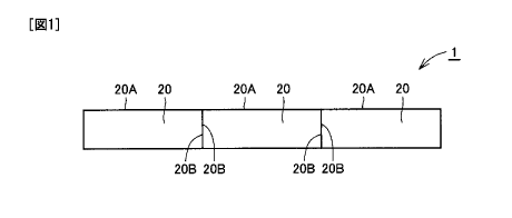
(First Embodiment)
First, one embodiment, i.e., a first embodiment of the present invention will
be
described with reference to Fig. 1 and Fig. 2. Fig. 1 corresponds to a cross
sectional
view taken along a line I-I in Fig. 2. Referring to Fig. 1, a silicon carbide
substrate I
of the present embodiment includes a plurality of SiC layers 20 each made of
single-
crystal silicon carbide and arranged side by side when viewed in a planar
view. The
plurality of SiC layers 20 have end surfaces 20B connected to one another.
In silicon carbide substrate 1 of the present embodiment, end surfaces 20B of
SiC layers 20 are connected to one another such that the plurality of SiC
layers 20 each
made of single-crystal silicon carbide are arranged side by side when viewed
in a planar
view. As such, silicon carbide substrate 1 effectively utilizes the SiC
substrates (SiC
layers) each obtained from a silicon carbide single-crystal having a small
diameter and
readily achieving high quality, whereby silicon carbide substrate 1 can be
handled as a
silicon carbide substrate excellent in crystallinity and having a large
diameter.
Further, referring to Fig. I and Fig. 2, in silicon carbide substrate 1, the
plurality
- 17-
CA 02759852 2011-10-24 110267:910421
of SiC layers 20 are arranged in the form of a matrix when viewed in a planar
view.
More specifically, adjacent ones of the plurality of SiC layers 20 are
disposed such that
their end surfaces 20B are in contact with each other. Explaining from a
different
point of view, end surfaces 20B of the adjacent ones of the plurality of SiC
layers 20 are
directly connected to each other. Accordingly, silicon carbide substrate 1 is
provided
with a larger area usable for manufacturing of semiconductor devices, as
compared with
a case where they are connected to each other with an intermediate layer
interposed
therebetween. Utilization of silicon carbide substrate 1 having such a large
diameter
allows for efficient manufacturing process of semiconductor devices. Further,
in
silicon carbide substrate 1, each of end surfaces 20B of SiC layers 20 is
perpendicular
to main surface 20A thereof. This allows SiC layers 20 to be readily arranged
in the
form of a matrix.
Further, as shown in Fig. 3, an epitaxial growth layer 30 made of single-
crystal
silicon carbide is formed on main surfaces 20A of SiC layers 20, thereby
fabricating a
silicon carbide substrate 2 including the epitaxial growth layer, which is
usable as a
buffer layer or an active layer.
Here, an impurity included in each of SiC layers 20 can be nitrogen or
phosphorus. In particular, by adopting phosphorus as the impurity, the
resistivity of
silicon carbide substrate I can become smaller than the resistivity thereof in
the case
where nitrogen is adopted as the impurity, with their impurity concentrations
being the
same.
Here, in silicon carbide substrate 1 described above, main surface 20A of each
of SiC substrates 20 may have an off angle of not less than 50 and not more
than 65
relative to the {0001 } plane. By fabricating a MOSFET using such a silicon
carbide
substrate 1, formation of interface states can be reduced in a channel region,
thereby
obtaining a MOSFET reduced in on-resistance. Meanwhile, in order to facilitate
the
manufacturing, main surface 20A of SiC layer 20 may correspond to the {0001}
plane.
Further, the off orientation of main surface 20A of SiC layer 20 may form an
-18-
CA 02759852 2011-10-24 110267:910421
angle of 5 or less relative to the <1-100> direction. The <1-100> direction
is a
representative off orientation in a silicon carbide substrate. Variation in
the off
orientation resulting from variation in a slicing process of the process of
manufacturing
the substrate is adapted to be 5 or smaller, which allows an epitaxial growth
layer to be
formed readily on silicon carbide substrate 1.
Further, in silicon carbide substrate 1, main surface 20A of SiC layer 20
preferably has an off angle of not less than -3 and not more than 5 relative
to the {03-
38} plane in the <1-100> direction. Accordingly, channel mobility can be
further
improved in the case where a MOSFET is fabricated using silicon carbide
substrate 1.
Alternatively, in silicon carbide substrate 1, the off orientation of main
surface
20A of SiC layer 20 may form an angle of 5 or smaller relative to the <11-20>
direction.
The <11-20> direction is a representative off orientation in a silicon carbide
substrate. Variation in the off orientation resulting from variation in a
slicing process
of the process of manufacturing the substrate is adapted to be 5 , which
allows an
epitaxial growth layer to be formed readily on silicon carbide substrate 1.
Further, it is desirable that SiC layer 20 has an impurity concentration of
more
than 5 x 10¹⁸Cm"3and less than 2 x 1019cm"3. In this way, the resistivity can
be reduced
while restraining stacking faults in SiC layer 20.
Further, SiC layer 20 preferably has a micro pipe density of not more than I
cm-
Z. Further, SiC layer 20 preferably has a dislocation density of not more than
1 X
104cm"2. Further, SiC layer 20 preferably has a stacking fault density of not
more than
0.1 cm-1. By employing such a high-quality SiC layer 20, yield can be improved
in
fabricating semiconductor devices using silicon carbide substrate 1.
The following describes an exemplary method for manufacturing silicon carbide
substrate 1 described above. Referring to Fig. 4, a substrate preparing step
is first
performed as a step (S 10) in the method for manufacturing the silicon carbide
substrate
in the present embodiment. In this step (S 10), referring to Fig. I and Fig.
2, the
-19-
CA 02759852 2011-10-24 110267:910421
plurality of SiC substrates 20 each of which is made of single-crystal silicon
carbide
and will be SiC layers 20 are prepared. Each of SiC substrates 20 has the main
surface,
which will be main surface 20A of SiC layer 20 that will be obtained by this
manufacturing method (see Fig. 1). Hence, on this occasion, the plane
orientation of
the main surface of SiC substrate 20 is selected in accordance with desired
plane
orientation of main surface 20A. Here, for example, a SiC substrate 20 having
a main
surface 20A corresponding to the {03-38} plane is prepared. Further, as SiC
substrate
20, a substrate is employed which has an impurity concentration of more than 5
x 1018
cm-3 and less than 2 x 1019 cm-3.
Next, as a step (S20), a contiguously arranging step is performed. In this
step
(S20), referring to Fig. 1 and Fig. 2, the plurality of SiC substrates 20
prepared in step
(S 10) are arranged side by side when viewed in a planar view such that end
surfaces
20B of adjacent SiC substrates 20 are in contact with each other.
Next, as a step (S30), a connecting step is performed. In this step (S30),
adjacent SiC substrates 20 are connected to each other by heating SiC
substrates 20
arranged in step (S20) such that end surfaces 20B of the adjacent ones are in
contact
with each other. This heating can be performed under reduced pressure (for
example,
in vacuum). With the above-described process, silicon carbide substrate I of
the first
embodiment is completed.
Further, by performing the following steps to form the epitaxial growth layer
on
silicon carbide substrate 1, silicon carbide substrate 2 described above may
be
fabricated. Namely, as a step (S40), a surface smoothing step is performed
onto
silicon carbide substrate 1 fabricated by performing steps (S 10)-(S30). In
this step
(S40), main surface 20A of each SiC substrate 20 is smoothed by, for example,
polishing. This allows a high-quality epitaxial growth layer to be formed on
main
surface 20A of SiC substrate 20.
Further, as a step (S50), an epitaxial growth step is performed. In this step
(S50), referring to Fig. 1 and Fig. 3, epitaxial growth layer 30 is formed on
SiC layers
-20-
CA 02759852 2011-10-24 110267:910421
20. In this way, silicon carbide substrate 2 is completed which includes
epitaxial
growth layer 30 usable as a buffer layer or an active layer in a semiconductor
device.
Here, in step (S20), a gap between adjacent SiC substrates 20 is preferably
not
more than 100 m. Even when end surfaces 20B of SiC substrates 20 are highly
flat, a
slight gap is formed between SiC substrates 20. If this gap is more than 100
m, a
state of connection between SiC substrates 20 may not become uniform. By
setting
the gap between SiC substrates 20 to be not more than 100 m, SiC substrates
20 can
be uniformly connected to each other more securely.
Further, in step (S30), it is preferable to heat SiC substrates 20 to fall
within a
range of temperature equal to or higher than the sublimation temperature of
silicon
carbide. This allows SiC substrates 20 to be connected to each other more
securely.
Further, heating temperature for SiC substrates 20 in step (S30) is preferably
not
less than 1800 C and not more than 2500 C. If the heating temperature is lower
than
1800 C, it takes a long time to connect SiC substrates 20 to one another,
which results
in decreased efficiency in manufacturing silicon carbide substrate 1. On the
other
hand, if the heating temperature exceeds 2500 C, surfaces of SiC substrates 20
become
rough, which may result in generation of a multiplicity of crystal defects in
silicon
carbide substrate 1 to be fabricated. In order to improve efficiency in
manufacturing
while restraining generation of defects in silicon carbide substrate 1, the
heating
temperature for SiC substrates 20 in step (S30) is preferably set at not less
than 1900 C
and not more than 2100 C. Further, when the pressure of atmosphere upon the
heating in step (S30) is set at not less than 10"5 Pa and not more than 106
Pa, they can be
connected to one another using a simple device. Further, in this step (S30),
the
plurality of SiC substrates may be heated under a pressure higher than 10-1 Pa
and lower
than 104 Pa, This can accomplish the above-described connection using a simple
device, and provide an atmosphere for accomplishing the connection for a
relatively
short time, thereby achieving reduced manufacturing cost of silicon carbide
substrate 1.
Further, the atmosphere upon the heating in step (S30) may be inert gas
atmosphere.
-21-
CA 02759852 2011-10-24 110267:910421
In the case where the atmosphere is the inert gas atmosphere, the inert gas
atmosphere
preferably contains at least one selected from a group consisting of argon,
helium, and
nitrogen. Further, in this step (S30), the plurality of SiC substrates 20 may
be heated
in an atmosphere obtained by reducing pressure of the atmospheric air. This
reduces
manufacturing cost of silicon carbide substrate 1.
Further, it has been illustrated in the above-described embodiment that: in
step
(S 10), there are prepared SiC substrates 20 each having main surface 20A
corresponding to the {03-38} plane; and in steps (S20) and (S30), they are
arranged
such that main surfaces 20A each corresponding to the {03-38} plane are in
alignment
with one another, i.e., main surfaces 20A corresponding to the {03-38} plane
are in
alignment with one another in one flat plane (in the case where each of main
surfaces
20A has an off orientation corresponding to the <1-100> direction). However,
instead
of this, each of main surfaces 20A may have an off orientation corresponding
to, for
example, the <11-20> direction.
Further, each of SiC substrates 20 prepared in step (S 10) preferably has a
micro
pipe density of not more than I cm-2. Further, each of SiC substrates 20
prepared in
step (S 10) preferably has a dislocation density of not more than I x 104cm-2.
Further,
each of SiC substrates 20 prepared in step (S 10) preferably has a stacking
fault density
of not more than 0.1 cm-1. By manufacturing silicon carbide substrate 1 with
such
high-quality SiC substrates 20 thus prepared, yield can be improved in
fabricating
semiconductor devices using silicon carbide substrate 1.
Further, each of SiC substrates 20 prepared in step (S 10) has an impurity
concentration of more than 5 x 1018 cm-3and less than 2 x 1019 cm-3. This
allows for
reduced resistivity while restraining stacking faults in each of SiC
substrates 20.
(Second Embodiment)
The following describes another embodiment of the present invention, i.e., a
second embodiment. Referring to Fig. 5 and Fig. 1, a silicon carbide substrate
1 in the
second embodiment has basically the same structure and provides basically the
same
-22-
CA 02759852 2011-10-24 110267:910421
effects as those of silicon carbide substrate 1 in the first embodiment.
However,
silicon carbide substrate I in the second embodiment is different from that of
the first
embodiment in that filling portions are provided to fill gaps between SiC
layers 20.
Referring to Fig. 5, silicon carbide substrate 2 in the second embodiment
further
includes filling portions 60 for filling the gaps between the plurality of SiC
layers 20.
Each of filling portions 60 may be made of, for example, silicon carbide or
silicon
dioxide. Further, a filling portion 60 made of silicon (Si) or made of a resin
may be
employed. Filling portion 60 made of Si can be formed by, for example,
introducing
melted Si into each gap between SiC layers 20. The intermediate layer made of
a resin
can be formed by, for example, pouring a melted resin into each gap between
SiC layers
and then performing appropriate hardening treatment to harden the resin.
Examples of the resin usable include an acrylic resin, an urethane resin,
polypropylene,
polystyrene, polyvinyl chloride, a resist, a SiC-containing resin, and the
like.
Accordingly, silicon carbide substrate I in the second embodiment restrains
foreign
15 matters such as abrasive particles from entering each gap between SiC
layers 20 even
when the surface thereof is polished.
It should be noted that each filling portion 60 has an impurity concentration
of
more than 5 x 1018 cm'3. This achieves reduced resistivity of filling portion
60,
thereby preventing the resistivity of silicon carbide substrate I from
increasing by
20 forming filling portion 60.
The following describes a method for manufacturing the silicon carbide
substrate in the second embodiment. Referring to Fig. 6, in the method for
manufacturing the silicon carbide substrate in this embodiment, steps (S10)-
(S30) are
performed in the same way as in the first embodiment. Accordingly, as shown in
Fig.
7, SiC substrates 20 are connected to one another at their end surfaces 20B.
Next, as a step (S31), a gap filling step is performed. In this step (S31),
the
filling portions are formed to fill the gaps between the plurality of SiC
substrates 20
connected to one another. Specifically, referring to Fig. 7 and Fig. 5, for
example, a
-23-
CA 02759852 2011-10-24 110267:910421
CVD epitaxial method is employed to grow silicon carbide, thereby forming
filling
portions 60 that fill the gaps between SiC substrates 20. It should be noted
that the
method for forming filling portions 60 is not limited to the CVD epitaxial
method, and
the sublimation method or liquid phase epitaxy may be employed, for example.
The
liquid phase epitaxy can be implemented by, for example, bringing SiC
substrates 20
into contact with a Si melt retained in a carbon crucible to supply them with
Si from the
melt and carbon from the crucible. Further, each of filling portions 60 is not
necessarily made of silicon carbide, and may be made of silicon dioxide, for
example.
A filling portion 60 made of silicon dioxide can be formed by, for example,
the CVD
method.
Next, as step (S40), the surface smoothing step is performed in the same way
as
in the first embodiment. On this occasion, filling portions 60 formed on main
surfaces
20A of SiC substrates 20 are removed by polishing. Further, filling portions
60 thus
formed prevent foreign matters such as abrasive particles from entering the
gaps
between SiC layers 20. With the above-described procedure, silicon carbide
substrate
1 in the second embodiment is completed as shown in Fig. 5. Further, as with
the first
embodiment, by performing step (S70), a silicon carbide substrate including an
epitaxial growth layer can be manufactured.
(Third Embodiment)
The following describes still another embodiment of the present invention,
i.e.,
a third embodiment. Referring to Fig. 8 and Fig. 1, a silicon carbide
substrate 1 in the
third embodiment has basically the same structure and provides basically the
same
effects as those of silicon carbide substrate 1 in the first embodiment.
However,
silicon carbide substrate 1 in the third embodiment is different from that of
the first
embodiment in terms of the shape of each of SiC layers 20.
Referring to Fig. 8, in the third embodiment, end surface 20B of each of SiC
layers 20 is not perpendicular to main surface 20A thereof. Further, end
surface 20B
of SiC layer 20 in the third embodiment corresponds to a cleavage plane. More
-24-
CA 02759852 2011-10-24 110267:910421
specifically, in the third embodiment, end surface 20B of SiC layer 20
corresponds to
the {0001 } plane.
The following describes a method for manufacturing silicon carbide substrate 1
in the third embodiment. Silicon carbide substrate I in the third embodiment
can be
manufactured in basically the same way as in the first embodiment. However,
the
method for manufacturing the silicon carbide substrate in the third embodiment
is
different from that in the first embodiment in terms of the shape of each of
SiC
substrates 20 prepared in step (S 10). Accordingly, a different manufacturing
method
from that in the first embodiment can be employed.
Namely, referring to Fig. 9, in the substrate preparing step performed as step
(S 10), SiC substrates 20 each corresponding to the shape of each SiC layer 20
in the
third embodiment is prepared. Specifically, end surface 20B of each of SiC
substrates
prepared in step (S 10) corresponds to the cleavage plane that is the { 0001 }
plane.
This restrains damages on a vicinity of the end surface of SiC substrate 20
when
15 obtaining SiC substrate 20. Asa result, crystallinity is maintained in the
vicinity of
the end surface of SiC substrate 20.
Next, referring to Fig. 9, a closely arranging step is performed as a step
(S21).
In this step (S21), referring to Fig. 10, adjacent SiC substrates 20 to be SiC
layers 20
(see Fig. 8) are held alternately by a first heater 81 and a second heater 82
disposed face
20 to face each other. On this occasion, an appropriate value of a space
between a SiC
substrate 20 held by first heater 81 and a SiC substrate 20 held by second
heater 82 is
considered to be associated with a mean free path for a sublimation gas
obtained upon
heating in a below-described step (S32). Specifically, the average value of
the space
can be set to be smaller than the mean free path for the sublimation gas
obtained upon
heating in the below-described step (S32). For example, strictly, a mean free
path for
atoms and molecules depends on atomic radius and molecule radius at a pressure
of 1
Pa and a temperature of 2000 C, but is approximately several cm to several ten
cm.
Hence, realistically, the space is preferably set at several cm or smaller.
More
-25-
CA 02759852 2011-10-24 110267:910421
specifically, SiC substrate 20 held by first heater 81 and SiC substrate 20
held by
second heater 82 are arranged close to each other such that their end surfaces
face each
other with a space of not less than I m and not more than 1 cm therebetween.
The
average value of the space is preferably 1 cm or smaller, more preferably, 1
mm or
smaller. Meanwhile, with the average value of the space being I .tm or
greater, there
can be secured a sufficient space for sublimation of silicon carbide. It
should be noted
that this sublimation gas is a gas formed by sublimation of solid silicon
carbide, and
includes Si, Si2C, and SiC2, for example. Further, first heater 81 is disposed
at an
upper side relative to second heater 82 (upper side in the vertical
direction).
Next, as step (S32), a sublimation step is performed. In this step (S32), SiC
substrates 20 are heated to a predetermined first temperature by first heater
81.
Likewise, SiC substrates 20 are heated to a predetermined second temperature
by
second heater 82. On this occasion, for example, by thus heating SiC
substrates 20
held by second heater 82 to the second temperature, SiC is sublimated from the
surfaces
of SiC substrates 20 held by second heater 82. The first temperature is set
lower than
the second temperature. Specifically, for example, the first temperature is
set lower
than the second temperature by not less than 1 C and not more than 100 C. The
first
temperature is preferably 1800 C or greater and 2500 C or smaller.
Accordingly, SiC
in the form of gas as a result of the sublimation from SiC substrates 20 held
by second
heater 82 reaches the surfaces of SiC substrates 20 held by first heater 81.
By
maintaining this state, adjacent SiC substrates (SiC layers) 20 are connected
to each
other at their end surfaces 20B as shown in Fig. 8, thus completing silicon
carbide
substrate 1 in the third embodiment. Further, as with the first embodiment, by
performing steps (S40) and (S50), a silicon carbide substrate including an
epitaxial
growth layer can be fabricated.
It should be noted that in the manufacturing method in the embodiment
described above, SiC substrate 20 held by first heater 81 and SiC substrate 20
held by
second heater 82 are arranged in step (S21) with an space therebetween, but
they may
-26-
. f e
CA 02759852 2011-10-24 110267:910421
be arranged without any space therebetween, i.e., arranged in contact with
each other.
Also in this case, a gap is formed between SiC substrate 20 held by first
heater 81 and
SiC substrate 20 held by second heater 82. In this gap, SiC is sublimated,
thereby
obtaining silicon carbide substrate 1 in the third embodiment.
(Fourth Embodiment)
The following describes yet another embodiment of the present invention, i.e.,
a
fourth embodiment. Referring to Fig. I1 and Fig. 1, a silicon carbide
substrate 1 in the
fourth embodiment has basically the same configuration and provides basically
the
same effects as those of silicon carbide substrate 1 in the first embodiment.
However,
silicon carbide substrate 1 in the fourth embodiment is different from that of
the first
embodiment in that amorphous SiC layers each serving as an intermediate layer
are
provided between adjacent SiC layers.
Namely, referring to Fig. 11, in silicon carbide substrate 1 in the fourth
embodiment, each of amorphous SiC layers 40 is provided between adjacent SiC
layers
20. Amorphous SiC layer 40 at least has a portion made of amorphous SiC, and
serves as an intermediate layer. Then, adjacent SiC layers 20 are connected to
each
other by this amorphous SiC layer 40. Amorphous SiC layer 40 thus existing
facilitates fabrication of silicon carbide substrate I in which adjacent SiC
layers 20 are
connected to each other. Here, a space between adjacent SiC layers 20, i.e.,
the
thickness of the intermediate layer (amorphous SiC layer 40) is preferably set
at 100 m
or smaller, more preferably, 10 m or smaller.
The following describes a method for manufacturing silicon carbide substrate 1
in the fourth embodiment. Referring to Fig. 12, in the method for
manufacturing
silicon carbide substrate I in the fourth embodiment, the substrate preparing
step is
performed as step (S 10) in the same way as in the first embodiment, so as to
prepare the
plurality of SiC substrates 20.
Next, a Si layer forming step is performed as a step (S 11). In this step (S I
I),
referring to Fig. 13, a Si layer 41 having a thickness of 100 nln is formed on
each of end
-27-
CA 02759852 2011-10-24 110267:910421
surfaces 20B of SiC substrates 20 prepared in step (S 10), for example. This
Si layer
41 can be formed using the sputtering method, for example.
Next, as step (S20), the contiguously arranging step is performed. In this
step
(S20), as with the first embodiment, adjacent SiC substrates 20 are arranged
side by
side in the form of a matrix such that they come into contact with Si layer 41
formed
therebetween in step (S 11).
Next, as a step (S33), a heating step is performed. In this step (S33), SiC
substrates 20 arranged to come into contact with Si layer 41 formed
therebetween is
heated, for example, in a mixed gas atmosphere of hydrogen gas and propane gas
under
a pressure of I x 103 Pa at approximately 1500 C for 3 hours. Accordingly, Si
layer
41 is supplied with carbon as a result of diffusion mainly from SiC substrates
20,
thereby forming amorphous SiC layer 40 as shown in Fig. 11. With the above-
described process, silicon carbide substrate 1 in the fourth embodiment can be
manufactured. Further, as with the first embodiment, by performing steps (S40)
and
(S50), a silicon carbide substrate including an epitaxial growth layer may be
fabricated.
(Fifth Embodiment)
The following describes still another embodiment of the present invention,
i.e.,
a fifth embodiment. Referring to Fig. 14, a silicon carbide substrate 1 in the
fifth
embodiment has basically the same configuration and provides basically the
same
effects as those of silicon carbide substrate 1 in the first embodiment.
However,
silicon carbide substrate 1 in the fifth embodiment is different from that of
the first
embodiment in-that an intermediate layer 70 are formed between adjacent SiC
layers 20.
More specifically, intermediate layer 70 includes carbon to serve as a
conductor.
Here, intermediate layer 70 usable herein includes, for example, graphite
particles and
non-graphitizable carbon. Preferably, intermediate layer 70 has a carbon
composite
structure including graphite particles and non-graphitizable carbon.
Namely, in silicon carbide substrate 1 of the fifth embodiment, intermediate
layer 70 serving as a conductor by including carbon therein is disposed
between
-28-
CA 02759852 2011-10-24 110267:910421
adjacent SiC layers 20. Adjacent SiC layers 20 are connected to each other via
intermediate layer 70. Intermediate layer 70 thus existing facilitates
fabrication of
silicon carbide substrate 1 in which adjacent SiC layers 20 are connected to
each other
at their end surfaces 20B.
The following describes a method for manufacturing silicon carbide substrate 1
in the fifth embodiment. Referring to Fig. 15, in the method for manufacturing
silicon
carbide substrate 1 in the fifth embodiment, step (S 10) is performed in the
same way as
in the first embodiment.
Next, as a step (S 12), an adhesive agent applying step is performed. In this
step (S 12), referring to Fig. 16, for example, a carbon adhesive agent is
applied to end
surfaces 20B of SiC substrates 20, thereby forming precursor layers 71. The
carbon
adhesive agent can be formed of, for example, a resin, graphite particles, and
a solvent.
Here, an exemplary resin usable is a resin formed into non-graphitizable
carbon by
heating, such as a phenol resin. An exemplary solvent usable is phenol,
formaldehyde,
ethanol, or the like. Further, the carbon adhesive agent is preferably applied
at an
amount of not less than 10 mg/cm2 and not more than 40 mg/cm2, more
preferably, at
an amount of not less than 20 mg/cm2and not more than 30 mg/cm2. Further, the
carbon adhesive agent applied preferably has a thickness of not more than 100
m,
more preferably, not more than 50 m.
Next, as step (S20), the contiguously arranging step is performed. In this
step
(S20), as with the first embodiment, referring to Fig. 16, adjacent SiC
substrates 20 are
arranged side by side in the form of a matrix such that they come into contact
with
precursor layer 71 formed therebetween in step (S 12).
Next, as a step (S34), a prebake step is performed. In this step (S34), SiC
substrates 20 arranged in contact with precursor layers 71 formed therebetween
are
heated, thereby removing a solvent component from the carbon adhesive agent
constituting each of precursor layers 71. Specifically, SiC substrates 20 are
gradually
heated to a range of temperature exceeding the boiling point of the solvent
component.
-29-
CA 02759852 2011-10-24 110267:910421
By performing this heating as long as possible, the adhesive agent is degassed
to
improve strength in adhesion.
Next, as a step (S35), a sintering step is performed. In this step (S35), SiC
substrates 20 with precursor layers 71 heated and accordingly prebaked in step
(S34)
are heated to a high temperature, preferably, not less than 900 C and not more
than
1100 C, for example, 1000 C for preferably not less than 10 minutes and not
more than
hours, for example, for 1 hour, thereby sintering precursor layers 71.
Atmosphere
employed upon the sintering can be an inert gas atmosphere such as argon. The
pressure of the atmosphere can be, for example, atmospheric pressure. In this
way,
10 precursor layers 71 are formed into intermediate layers 70 each made of
carbon that is a
conductor. With the above-described process, silicon carbide substrate 1 in
the fifth
embodiment can be manufactured. Further, as with the first embodiment, by
performing steps (S40) and (S50), a silicon carbide substrate including an
epitaxial
growth layer may be fabricated.
It should be noted that the fourth and fifth embodiments has illustrated the
intermediate layers including amorphous SiC and carbon respectively, but the
intermediate layer is not limited to these. Instead of these, an intermediate
layer made
of a metal can be employed, for example. In this case, as the metal, it is
preferable to
employ a metal that can make ohmic contact with silicon carbide by forming a
silicide,
such as nickel.
(Sixth Embodiment)
As a sixth embodiment, the following describes one exemplary semiconductor
device fabricated using the above-described silicon carbide substrate of the
present
invention. Referring to Fig. 17, a semiconductor device 101 according to the
present
invention is a DiMOSFET (Double Implanted MOSFET) of vertical type, and has a
substrate 102, a buffer layer 121, a reverse breakdown voltage holding layer
122, p
regions 123, n+ regions 124, p+ regions 125, an oxide film 126, source
electrodes 111,
upper source electrodes 127, a gate electrode 110, and a drain electrode 112
formed on
-30-
CA 02759852 2011-10-24 110267:910421
the backside surface of substrate 102. Specifically, buffer layer 121 made of
silicon
carbide is formed on the front-side surface of substrate 102 made of silicon
carbide of n
type conductivity. As substrate 102, there is employed a silicon carbide
substrate of
the present invention, inclusive of silicon carbide substrates I in the first
to fifth
embodiments. In the case where silicon carbide substrate I in each of the
first to fifth
embodiments is employed, buffer layer 121 is formed on SiC layers 20 of
silicon
carbide substrate 1. Buffer layer 121 has n type conductivity, and has a
thickness of,
for example, 0.5 m. Further, impurity with n type conductivity in buffer
layer 121
has a concentration of, for example, 5 x 1017 cm"3. Formed on buffer layer 121
is
reverse breakdown voltage holding layer 122. Reverse breakdown voltage holding
layer 122 is made of silicon carbide of n type conductivity, and has a
thickness of 10
m, for example. Further, reverse breakdown voltage holding layer 122 includes
an
impurity of n type conductivity at a concentration of, for example, 5 x 10¹⁵
cm"3.
Reverse breakdown voltage holding layer 122 has a surface in which p regions
123 of p type conductivity are formed with a space therebetween. In each of p
regions
123, an n+ region 124 is formed at the surface layer of p region 123. Further,
at a
location adjacent to n+ region 124, a p+ region 125 is formed. Oxide film 126
is
formed to extend on n+ region 124 in one p region 123, p region 123, an
exposed
portion of reverse breakdown voltage holding layer 122 between the two p
regions 123,
the other p region 123, and n+ region 124 in the other p region 123. On oxide
film 126,
gate electrode 110 is formed. Further, source electrodes 111 are formed on n+
regions
124 and p+ regions 125. On source electrodes 111, upper source electrodes 127
are
formed. Moreover, drain electrode 112 is formed on the backside surface of
substrate
102, i.e., the surface opposite to its front-side surface on which buffer
layer 121 is
formed.
Semiconductor device 101 in the present embodiment employs, as substrate 102,
the silicon carbide substrate in the present invention such as silicon carbide
substrate 1
described in each of the first to fifth embodiments. Here, as described above,
the
-31-
CA 02759852 2011-10-24 110267:910421
silicon carbide substrate of the present invention is a silicon carbide
substrate excellent
in crystallinity and having a large diameter. Hence, semiconductor device 101
is a
semiconductor device in which buffer layer 121 and reverse breakdown voltage
holding
layer 122 formed on substrate 102 as epitaxial layers are excellent in
crystallinity, and is
manufactured with reduced cost.
The following describes a method for manufacturing semiconductor device 101
shown in Fig. 17, with reference to Fig. 18-Fig. 22. Referring to Fig. 18,
first, a
substrate preparing step (S] 10) is performed. Prepared here is, for example,
substrate
102, which is made of silicon carbide and has its main surface corresponding
to the (03-
38) plane (see Fig. 19). As substrate 102, there is prepared a silicon carbide
substrate
of the present invention, inclusive of silicon carbide substrate 1
manufactured in
accordance with each of the manufacturing methods described in the first to
fifth
embodiments.
Alternatively, as substrate 102 (see Fig. 19), a substrate may be employed
which
has n type conductivity and has a substrate resistance of 0.02 acm.
Next, as shown in Fig. 18, an epitaxial layer forming step (S 120) is
performed.
Specifically, buffer layer 121 is formed on the front-side surface of
substrate 102.
Buffer layer 121 is formed on SiC layers 20 (see Fig. 1, Fig. 5, Fig. 8, Fig.
11, and Fig.
14) of silicon carbide substrate I employed as substrate 102. As buffer layer
121, an
epitaxial layer is formed which is made of silicon carbide of n type
conductivity and has
a thickness of 0.5 m, for example. Buffer layer 121 has a conductive impurity
at a
concentration of, for example, 5 x 1017 cm"3. Then, on buffer layer 121,
reverse
breakdown voltage holding layer 122 is formed as shown in Fig. 19. As reverse
breakdown voltage holding layer 122, a layer made of silicon carbide of n type
conductivity is formed using an epitaxial growth method. Reverse breakdown
voltage
holding layer 122 can have a thickness of, for example, 10 m. Further,
reverse
breakdown voltage holding layer 122 includes an impurity of n type
conductivity at a
concentration of, for example, 5 X 1015 cm 3.
-32-
CA 02759852 2011-10-24 110267:910421
Next, as shown in Fig. 18, an implantation step (S 130) is performed.
Specifically, an impurity of p type conductivity is implanted into reverse
breakdown
voltage holding layer 122 using, as a mask, an oxide film formed through
photolithography and etching, thereby forming p regions 123 as shown in Fig.
20.
Further, after removing the oxide film thus used, an oxide film having a new
pattern is
formed through photolithography and etching. Using this oxide film as a mask,
a
conductive impurity of n type conductivity is implanted into predetermined
regions to
form n+ regions 124. In a similar way, a conductive impurity of p type
conductivity is
implanted to form p+ regions 125. As a result, the structure shown in Fig. 20
is
obtained.
After such an implantation step, an activation annealing process is performed.
This activation annealing process can be performed under conditions that, for
example,
argon gas is employed as atmospheric gas, heating temperature is set at 1700
C, and
heating time is set at 30 minutes.
Next, a gate insulating film forming step (S 140) is performed as shown in
Fig.
18. Specifically, as shown in Fig. 21, oxide film 126 is formed to cover
reverse
breakdown voltage holding layer 122, p regions 123, n+ regions 124, and p+
regions 125.
As a condition for forming oxide film 126, for example, dry oxidation (thermal
oxidation) may be performed. The dry oxidation can be performed under
conditions
that the heating temperature is set at 1200 C and the heating time is set at
30 minutes.
Thereafter, a nitrogen annealing step (S 150) is performed as shown in Fig.
18.
Specifically, an annealing process is performed in atmospheric gas of nitrogen
monoxide (NO). Temperature conditions for this annealing process are, for
example,
as follows: the heating temperature is 1100 C and the heating time is 120
minutes. As
a result, nitrogen atoms are introduced into a vicinity of the interface
between oxide
film 126 and each of reverse breakdown voltage holding layer 122, p regions
123, n+
regions 124, and p+ regions 125, which are disposed below oxide film 126.
Further,
after the annealing step using the atmospheric gas of nitrogen monoxide,
additional
-33-
CA 02759852 2011-10-24 110267:910421
annealing may be performed using argon (Ar) gas, which is an inert gas.
Specifically,
using the atmospheric gas of argon gas, the additional annealing may be
performed
under conditions that the heating temperature is set at 1100 C and the heating
time is
set at 60 minutes.
Next, as shown in Fig. 18, an electrode forming step (S 160) is performed.
Specifically, a resist film having a pattern is formed on oxide film 126 by
means of the
photolithography method. Using the resist film as a mask, portions of the
oxide film
above n+ regions 124 and p+ regions 125 are removed by etching. Thereafter, a
conductive film such as a metal is formed on the resist film and formed in
openings of
oxide film 126 in contact with n+ regions 124 and p+ regions 125. Thereafter,
the
resist film is removed, thus removing the conductive film's portions located
on the
resist film (lift-off). Here, as the conductor, nickel (Ni) can be used, for
example.
As a result, as shown in Fig. 22, source electrodes 111 and drain electrode
112 can be
obtained. It should be noted that on this occasion, heat treatment for
alloying is
preferably performed. Specifically, using atmospheric gas of argon (Ar) gas,
which is
an inert gas, the heat treatment (alloying treatment) is performed with the
heating
temperature being set at 950 C and the heating time being set at 2 minutes.
Thereafter, on source electrodes 111, upper source electrodes 127 (see Fig.
17)
are formed. Further, drain electrode 112 (see Fig. 17) is formed on the
backside
surface of substrate 102. Further, gate electrode 110 (see Fig. 17) is formed
on oxide
film 126. In this way, semiconductor device 101 shown in Fig. 17 can be
obtained.
Namely, semiconductor device 101 is fabricated by forming the epitaxial layers
and the
electrodes on SiC layers 20 of silicon carbide substrate 1.
It should be noted that in the sixth embodiment, the vertical type MOSFET has
been illustrated as one exemplary semiconductor device that can be fabricated
using the
silicon carbide substrate of the present invention, but the semiconductor
device that can
be fabricated is not limited to this. For example, various types of
semiconductor
devices can be fabricated using the silicon carbide substrate of the present
invention,
-34-
CA 02759852 2011-10-24 110267:910421
such as a JFET (Junction Field Effect Transistor), an IGBT (Insulated Gate
Bipolar
Transistor), and a Schottky barrier diode. Further, the sixth embodiment has
illustrated a case where the semiconductor device is fabricated by forming the
epitaxial
layer, which serves as an active layer, on the silicon carbide substrate
having its main
surface corresponding to the (03-38) plane. However, the crystal plane that
can be
adopted for the main surface is not limited to this and any crystal plane
suitable for the
purpose of use and including the (0001) plane can be adopted for the main
surface.
As described in the sixth embodiment, a semiconductor device can be fabricated
using the silicon carbide substrate of the present invention. Specifically, in
the
semiconductor device of the present invention, on the silicon carbide
substrate of the
present invention, an epitaxial layer is formed as an active layer. More
specifically,
the semiconductor device of the present invention includes: the silicon
carbide substrate
of the present invention; an epitaxial growth layer formed on the silicon
carbide
substrate; and an electrode formed on the epitaxial layer. In other words, the
semiconductor device of the present invention includes: a plurality of SiC
layers made
of single-crystal silicon carbide and arranged side by side when viewed in a
planar
view; an epitaxial growth layer formed on the SiC layers; and an electrode
formed on
the epitaxial layer, the plurality of SiC layers having end surfaces connected
to one
another.
The embodiments disclosed herein are illustrative and non-restrictive in any
respect. The scope of the present invention is defined by the terms of the
claims,
rather than the embodiments described above, and is intended to include any
modifications within the scope and meaning equivalent to the terms of the
claims.
INDUSTRIAL APPLICABILITY
A method for manufacturing a silicon carbide substrate, and the silicon
carbide
substrate in the present invention are particularly advantageously applicable
to a
method for manufacturing a silicon carbide substrate required to have both
high
crystallinity and a large diameter, as well as such a silicon carbide
substrate.
CA 02759852 2011-10-24 110267:910421
REFERENCE SIGNS LIST
1, 2: silicon carbide substrate; 20: SiC layer (SiC substrate); 20A: main
surface;
20B: end surface; 30: epitaxial growth layer; 40: amorphous SiC layer; 41: Si
layer; 60:
filling portion; 70: intermediate layer; 71: precursor layer; 81: first
heater; 82: second
heater; 101: semiconductor device; 102: substrate; 110: gate electrode; 111:
source
electrode; 112: drain electrode; 121: buffer layer; 122: reverse breakdown
voltage
holding layer; 123: p region; 124: n+ region; 125: p+ region; 126: oxide film;
127: upper
source electrode,
-36-