Note: Descriptions are shown in the official language in which they were submitted.
CA 02759861 2011-10-24 110277:910431
DESCRIPTION
TITLE OF INVENTION
Method for Manufacturing Silicon Carbide Substrate and Silicon Carbide
Substrate
TECHNICAL FIELD
The present invention relates to a method for manufacturing a silicon carbide
substrate, and the silicon carbide substrate, more particularly, a method for
manufacturing a silicon carbide substrate, and the silicon carbide substrate,
each of
which achieves reduced cost of manufacturing a semiconductor device using the
silicon
carbide substrate.
BACKGROUND ART
In recent years, in order to achieve high breakdown voltage, low loss, and
utilization of semiconductor devices under a high temperature environment,
silicon
carbide (SiC) has begun to be adopted as a material for a semiconductor
device.
Silicon carbide is a wide band gap semiconductor having a band gap larger than
that of
silicon, which has been conventionally widely used as a material for
semiconductor
devices. Hence, by adopting silicon carbide as a material for a semiconductor
device,
the semiconductor device can have a high breakdown voltage, reduced on-
resistance,
and the like. Further, the semiconductor device thus adopting silicon carbide
as its
material has characteristics less deteriorated even under a high temperature
environment than those of a semiconductor device adopting silicon as its
material,
advantageously.
Under such circumstances, various studies have been conducted on methods for
manufacturing silicon carbide crystals and silicon carbide substrates used for
manufacturing of semiconductor devices, and various ideas have been proposed
(for
example, see M. Nakabayashi, et al., "Growth of Crack-free 100mm-diameter 4H-
SiC
Crystals with Low Micropipe Densities, Mater. Sci. Forum, vols. 600-603, 2009,
p.3-6
-1-
CA 02759861 2011-10-24 110277:910431
(Non-Patent Literature 1)).
CITATION LIST
NON PATENT LITERATURE
NPL 1: M. Nakabayashi, et al., "Growth of Crack-free 100 mm-diameter 4H-
SiC Crystals with Low Micropipe Densities, Mater. Sci. Forum, vols. 600-603,
2009,
p.3-6
SUMMARY OF INVENTION
TECHNICAL PROBLEM
However, silicon carbide does not have a liquid phase at an atmospheric
pressure. In addition, crystal growth temperature thereof is 2000 C or
greater, which
is very high. This makes it difficult to control and stabilize growth
conditions.
Accordingly, it is difficult for a silicon carbide single-crystal to have a
large diameter
while maintaining its quality to be high. Hence, it is not easy to obtain a
high-quality
silicon carbide substrate having a large diameter. This difficulty in
fabricating such a
silicon carbide substrate having a large diameter results in not only
increased
manufacturing cost of the silicon carbide substrate but also fewer
semiconductor
devices produced for one batch using the silicon carbide substrate.
Accordingly,
manufacturing cost of the semiconductor devices is increased,
disadvantageously. It is
considered that the manufacturing cost of the semiconductor devices can be
reduced by
effectively utilizing a silicon carbide single-crystal, which is high in
manufacturing cost,
as a substrate.
In view of this, an object of the present invention is to provide a method for
manufacturing a silicon carbide substrate, and the silicon carbide substrate,
each of
which achieves reduced cost of manufacturing a semiconductor device using the
silicon
carbide substrate.
SOLUTION TO PROBLEM
A method for manufacturing a silicon carbide substrate in the present
invention
includes the steps of: preparing a base substrate made of silicon carbide and
a SiC
-2-
CA 02759861 2011-10-24 110277:910431
substrate made of single-crystal silicon carbide; forming a Si film made of
silicon on
and in contact with a main surface of the base substrate; fabricating a
stacked substrate
by placing the SiC substrate on and in contact with the Si film; and
connecting the base
substrate and the SiC substrate to each other by heating the stacked substrate
to convert,
into silicon carbide, at least a region making contact with the base substrate
and a
region making contact with the SiC substrate in the Si film.
As described above, it is difficult for a high-quality silicon carbide single-
crystal
to have a large diameter. Meanwhile, for efficient manufacturing in a process
of
manufacturing a semiconductor device using a silicon carbide substrate, a
substrate
provided with predetermined uniform shape and size is required. Hence, even
when a
high-quality silicon carbide single-crystal (for example, silicon carbide
single-crystal
having a small defect density) is obtained, a region that cannot be processed
into such a
predetermined shape and the like by cutting, etc., may not be effectively
used.
To address this, in the method for manufacturing the silicon carbide substrate
of
the present invention, the SiC substrate made of single-crystal silicon
carbide different
from that of the base substrate is connected onto the base substrate. Thus,
the silicon
carbide substrate can be manufactured, for example, in the following manner.
That is,
the base substrate formed of low-quality silicon carbide crystal having a
large defect
density is processed to have the predetermined shape and size. On such a base
substrate, a high-quality silicon carbide single-crystal not shaped into the
predetermined
shape and the like is employed as the SiC substrate. Then, they are connected
to each
other. The silicon carbide substrate manufactured through such a process has
the
predetermined uniform shape and size, thereby achieving efficient
manufacturing of
semiconductor devices. Further, the silicon carbide substrate manufactured
through
such a process utilizes the SiC substrate formed of high-quality silicon
carbide single-
crystal and having not been used because it cannot be processed into a desired
shape
and the like conventionally. Using such a silicon carbide substrate,
semiconductor
devices can be manufactured, thereby effectively using silicon carbide single-
crystal.
-3-
CA 02759861 2011-10-24 110277:910431
Furthermore, in the method for manufacturing the silicon carbide substrate in
the
present invention, at least the portions of the Si film are converted into
silicon carbide,
thereby obtaining an intermediate layer allowing the base substrate and the
SiC
substrate to be firmly connected to each other. Hence, the silicon carbide
substrate
can be handled as one freestanding substrate. As such, according to the method
for
manufacturing the silicon carbide substrate in the present invention, there
can be
manufactured a silicon carbide substrate that allows for reduced cost of
manufacturing
semiconductor devices using the silicon carbide substrate.
Preferably, the method for manufacturing the silicon carbide substrate further
includes the step of smoothing at least one of main surfaces of the base
substrate and
the SiC substrate, which are to be disposed face to face with each other with
the Si film
interposed therebetween in the step of fabricating the stacked substrate, the
step of
smoothing being performed before the step of fabricating the stacked
substrate.
Thus, the surface to serve as the connection surface is smoothed in advance,
thereby allowing the base substrate and the SiC substrate to be connected to
each other
more securely. In order to attain further secure connection between the base
substrate
and the SiC substrate, it is preferable to smooth both the main surfaces of
the base
substrate and the SiC substrate, which are to be disposed face to face with
the Si film
interposed therebetween in the step of fabricating the stacked substrate.
Preferably, in the method for manufacturing the silicon carbide substrate, the
Si
film formed in the step of forming the Si film has a thickness of not less
than 10 nm
and not more than 1 m.
If the thickness of the Si film formed on the base substrate is less than 10
nm
and surface smoothness of each of the surfaces of the base substrate and the
SiC
substrate is not sufficiently high, the Si film to be formed between the base
substrate
and the SiC substrate becomes discontinuous, which may result in failure in
achieving
firm connection between the base substrate and the SiC substrate. In contrast,
if the
thickness of the Si film is more than I m, the thickness of the intermediate
layer (layer
-4-
CA 02759861 2011-10-24 110277:910431
obtained by converting at least the portions of the Si film into silicon
carbide) in the
thickness of the silicon carbide substrate to be manufactured becomes large.
This may
result in decreased characteristics particularly when fabricating a vertical
type device in
which a current flows in the thickness direction of silicon carbide substrate
1. Hence,
the Si film formed preferably has a thickness of not less than 10 nm and not
more than
1 m.
Preferably, in the method for manufacturing the silicon carbide substrate, in
the
step of connecting the base substrate and the SiC substrate to each other, the
stacked
substrate is heated in an atmosphere including a gas containing carbon.
Accordingly, carbon is supplied to the Si film not only from the base
substrate
and the SiC substrate but also from the atmosphere, thereby achieving
efficient
conversion of silicon of the Si film into silicon carbide.
Preferably, in the method for manufacturing the silicon carbide substrate, in
the
step of fabricating the stacked substrate, a plurality of the SiC substrates
are arranged
side by side when viewed in a planar view.
As described above, it is difficult for a high-quality silicon carbide single-
crystal
to have a large diameter. To address this, the plurality of SiC substrates
each obtained
from a high-quality silicon carbide single-crystal are arranged side by side
on the base
substrate having a large diameter when viewed in a planar view, thereby
obtaining a
silicon carbide substrate that can be handled as a substrate having a high-
quality SiC
layer and a large diameter. By using such a silicon carbide substrate, the
process of
manufacturing a semiconductor device can be improved in efficiency. It should
be
noted that in order to further improve the efficiency of the process of
manufacturing a
semiconductor device, it is preferable that adjacent ones of the plurality of
SiC
substrates are arranged in contact with one another. More specifically, for
example,
the plurality of SiC substrates are preferably arranged in contact with one
another in the
form of a matrix.
In the method for manufacturing the silicon carbide substrate, in the stacked
-5-
CA 02759861 2011-10-24 110277:910431
substrate, a main surface of the SiC substrate opposite to the base substrate
has an off
angle of not less than 50 and not more than 65 relative to a {0001 } plane.
By growing single-crystal silicon carbide of hexagonal system in the <0001>
direction, a high-quality single-crystal can be fabricated efficiently. From
such a
silicon carbide single-crystal grown in the <0001> direction, a silicon
carbide substrate
having a main surface corresponding to the {0001 } plane can be obtained
efficiently.
Meanwhile, by using a silicon carbide substrate having a main surface having
an off
angle of not less than 50 and not more than 65 relative to the plane
orientation of
{0001 }, a semiconductor device with high performance may be manufactured.
Specifically, for example, it is general that a silicon carbide substrate used
for
fabrication of a MOSFET has a main surface having an off angle of
approximately 8
relative to the plane orientation of {0001 }. An epitaxial growth layer is
formed on
this main surface and an oxide film, an electrode, and the like are formed on
this
epitaxial growth layer, thereby obtaining a MOSFET. In this MOSFET, a channel
region is formed in a region including an interface between the epitaxial
growth layer
and the oxide film. However, in the MOSFET having such a structure, a
multiplicity
of interface states are formed around the interface between the epitaxial
growth layer
and the oxide film, i.e., the location in which the channel region is formed,
due to the
substrate's main surface having an off angle of approximately 8 relative to
the {0001 }
plane. This hinders traveling of carriers, thus decreasing channel mobility.
To address this, in the stacked substrate, by setting the main surface of the
SiC
substrate opposite to the base substrate to have an off angle of not less than
50 and not
more than 65 relative to the {0001 } plane, the silicon carbide substrate to
be
manufactured will have a main surface having an off angle of not less than 50
and not
more than 65 relative to the {0001 } plane. This reduces formation of
interface states.
Hence, a MOSFET with reduced on-resistance can be fabricated.
In the method for manufacturing the silicon carbide substrate, in the stacked
substrate, the main surface of the SiC substrate opposite to the base
substrate has an off
-6-
CA 02759861 2011-10-24 110277:910431
orientation forming an angle of not more than 5 relative to the <1-100>
direction.
The <1-100> direction is a representative off orientation in a silicon carbide
substrate. Variation in the off orientation resulting from variation in a
slicing process
of the process of manufacturing the substrate is adapted to be not more than 5
, which
allows an epitaxial growth layer to be formed readily on the silicon carbide
substrate.
In the above-described method for manufacturing the silicon carbide substrate,
in the stacked substrate, the main surface of the SiC substrate opposite to
the base
substrate can have an off angle of not less than -3 and not more than 5
relative to a
{03-38} plane in the <1-100> direction.
Accordingly, channel mobility can be further improved in the case where a
MOSFET is fabricated using the silicon carbide substrate. Here, setting the
off angle
at not less than -3 and not more than +5 relative to the plane orientation
of {03-38} is
based on a fact that particularly high channel mobility was obtained in this
set range as
a result of inspecting a relation between the channel mobility and the off
angle.
Further, the "off angle relative to the {03-38} plane in the <1-100>
direction"
refers to an angle formed by an orthogonal projection of a normal line of the
above-
described main surface to a flat plane defined by the <1-100> direction and
the <0001 >
direction, and a normal line of the {03-38} plane. The sign of positive value
corresponds to a case where the orthogonal projection approaches in parallel
with the
<1-100> direction whereas the sign of negative value corresponds to a case
where the
orthogonal projection approaches in parallel with the <0001> direction.
It should be noted that the main surface preferably has a plane orientation of
substantially {03-38}, and the main surface more preferably has a plane
orientation of
{03-38}. Here, the expression "the main surface has a plane orientation of
substantially {03-38}" is intended to encompass a case where the plane
orientation of
the main surface of the substrate is included in a range of off angle such
that the plane
orientation can be substantially regarded as {03-38} in consideration of
processing
accuracy of the substrate. In this case, the range of off angle is, for
example, a range
-7-
CA 02759861 2011-10-24 110277:910431
of off angle of 2 relative to {03-38}. Accordingly, the above-described
channel
mobility can be further improved.
In the method for manufacturing the silicon carbide substrate, in the stacked
substrate, the main surface of the SiC substrate opposite to the base
substrate has an off
orientation forming an angle of not more than 5 relative to the <11-20>
direction.
The <11-20> direction is a representative off orientation in a silicon carbide
substrate, as with the <1-100> direction. Variation in the off orientation
resulting
from variation in the slicing process of the process of manufacturing the
substrate is
adapted to be 5 , which allows an epitaxial growth layer to be formed readily
on the
SiC substrate.
In the method for manufacturing the silicon carbide substrate, the base
substrate
may be made of single-crystal silicon carbide, and in the step of fabricating
the stacked
substrate, the stacked substrate may be fabricated such that main surfaces of
the base
substrate and the SiC substrate, which are disposed face to face with each
other with the
Si film interposed therebetween, have the same plane orientation.
A thermal expansion coefficient of single-crystal silicon carbide is
anisotropic
depending on its crystal plane. Hence, when surfaces corresponding to crystal
planes
greatly different from each other in thermal expansion coefficient are
connected to each
other, stress resulting from the difference in thermal expansion coefficient
is applied
between the base substrate and the SiC substrate. This stress may cause
strains or
cracks of the silicon carbide substrate in the manufacturing of the silicon
carbide
substrate or in the process of manufacturing semiconductor devices using the
silicon
carbide substrate. To address this, the silicon carbide single-crystals to
constitute the
above-described connection surface are adapted to have the same plane
orientation,
thereby reducing the stress. It should be noted that the state-in which "the
main
surfaces of the base substrate and the SiC substrate have the same plane
orientation"
does not need to correspond to a state in which the plane orientations of the
main
surfaces are strictly the same, and may correspond to a state in which they
are
-8-
CA 02759861 2011-10-24 110277:910431
substantially the same. More specifically, when the crystal plane constituting
the main
surface of the base substrate forms an angle of not more than 1 relative to
the crystal
plane constituting the main surface of the SiC substrate, it can be said that
the main
surfaces of the base substrate and the SiC substrate has substantially the
same plane
orientation.
In the method for manufacturing the silicon carbide substrate, in the stacked
substrate, the main surface of the SiC substrate opposite to the base
substrate has an off
angle of not less than 1 and not more than 60 relative to the {0001 }
plane.
By growing a silicon carbide single-crystal of hexagonal system in the <0001>
direction as described above, a high-quality single-crystal can be fabricated
efficiently.
From such a silicon carbide single-crystal grown in the <0001> direction, SiC
substrates can be obtained relatively effectively so far as the surface does
not have a
large off angle relative to the {0001 } plane, specifically, has an off angle
of 60 or
smaller. Meanwhile, with the off angle being 1 or greater, a high-quality
epitaxial
growth layer can be formed on such a SiC substrate.
In the method for manufacturing the silicon carbide substrate, the step of
connecting the base substrate and the SiC substrate to each other is performed
without
polishing main surfaces of the base substrate and the SiC substrate before the
step of
connecting the base substrate and the SiC substrate to each other, the main
surfaces of
the base substrate and the SiC substrate being to be disposed face to face
with each
other in the step of connecting the base substrate and the SiC substrate to
each other.
Accordingly, the manufacturing cost of the silicon carbide substrate can be
reduced. Here, as described above, the main surfaces of the base substrate and
the SiC
substrate, which are to be disposed face to face with each other in the step
of
connecting the base substrate and the SiC substrate to each other, may not be
polished.
However, for removal of damaged layers in the vicinity of surfaces formed by
slicing
upon fabricating the substrate, it is preferable to perform the step of
connecting the base
substrate and the SiC substrate to each other, after performing a step of
removing the
-9-
CA 02759861 2011-10-24 110277:910431
damaged layers by means of etching, for example.
The method for manufacturing the silicon carbide substrate may further include
the step of polishing a main surface of the SiC substrate, the main surface
corresponding to a main surface of the SiC substrate to be opposite to the
base substrate.
This allows a high-quality epitaxial growth layer to be formed on the main
surface of the SiC substrate opposite to the base substrate. As a result, a
semiconductor device can be manufactured which includes the high-quality
epitaxial
growth layer as an active layer, for example. Namely, by employing such a
step, a
silicon carbide substrate can be obtained which allows for manufacturing of a
high-
quality semiconductor device including the epitaxial growth layer formed on
the SiC
substrate. Here, the main surface of the SiC substrate may be polished after
connecting the base substrate and the SiC substrate to each other, or before
connecting
the base substrate and the SiC substrate to each other by previously polishing
the main
surface of the SiC substrate, which is to be opposite to the base substrate.
A silicon carbide substrate according to the present invention includes: a
base
layer made of silicon carbide; an intermediate layer formed on and in contact
with the
base layer; and a SiC layer made of single-crystal silicon carbide and
disposed on and in
contact with the intermediate layer. The intermediate layer contains silicon
carbide at
least at its region adjacent to the base layer and its region adjacent to the
SiC layer and
connects the base layer and the SiC layer to each other. The silicon carbide
in the
region adjacent to the base layer and the region adjacent to the SiC layer may
be
amorphous.
In the silicon carbide substrate of the present invention, the SiC layer made
of
single-crystal silicon carbide different from that of the base layer is
connected onto the
base layer. Hence, for example, a low-quality silicon carbide crystal having a
large
defect density is processed into predetermined shape and size suitable for
manufacturing of semiconductor devices to serve as the base layer, whereas a
high-
quality silicon carbide single-crystal having a suitable shape and the like
for
-10-
CA 02759861 2011-10-24 110277:910431
manufacturing of semiconductor devices is disposed on the base layer as the
SiC layer.
Such a silicon carbide substrate have the predetermined uniform shape and
size, thus
attaining effective manufacturing of semiconductor devices. Further,
semiconductor
devices can be manufactured using such a silicon carbide substrate that
employs the
high-quality SiC layer thus having a difficulty in being processed into the
shape and the
like suitable for manufacturing of semiconductor devices, thereby effectively
utilizing
the silicon carbide single-crystal. Further, in the silicon carbide substrate
of the
present invention, the base layer and the SiC layer are connected to each
other and are
unified by the intermediate layer containing silicon carbide at its region
adjacent to the
base layer and its region adjacent to the SiC layer. Hence, the silicon
carbide substrate
can be handled as one freestanding substrate. As such, according to the
silicon carbide
substrate of the present invention, there can be provided a silicon carbide
substrate
allowing for reduced cost of manufacturing semiconductor devices using the
silicon
carbide substrate.
In the silicon carbide substrate, preferably, a plurality of the SiC layers
are
arranged side by side when viewed in a planar view.
Thus, the plurality of SiC layers each obtained from a high-quality silicon
carbide single-crystal are arranged side by side on the base layer having a
large
diameter when viewed in a planar view, thereby obtaining a silicon carbide
substrate
that can be handled as a substrate having a high-quality SiC layer and a large
diameter.
By using such a silicon carbide substrate, the process of manufacturing a
semiconductor
device can be improved in efficiency. It should be noted that in order to
improve the
efficiency of the process of manufacturing a semiconductor device, it is
preferable that
adjacent ones of the plurality of SiC layers are arranged in contact with one
another.
More specifically, for example, the plurality of SiC layers are preferably
arranged in
contact with one another in the form of a matrix.
In the silicon carbide substrate, the base layer may be made of single-crystal
silicon carbide. In this case, no micro pipe of the base layer is preferably
propagated
-11-
CA 02759861 2011-10-24 110277:910431
to the SiC layer.
As the base layer, single-crystal silicon carbide having relatively many
defects
such as micro pipes can be employed. In employing it, the micro pipes formed
in the
base layer are prevented from being propagated to the SiC layer, thereby
allowing a
high-quality epitaxial growth layer to be formed on the SiC layer. The silicon
carbide
substrate of the present invention can be fabricated by connecting a
separately grown
SiC layer onto the base layer instead of directly growing the SiC layer on the
base layer.
Thus, the micro pipes formed in the base layer can be readily prevented from
being
propagated to the SiC layer.
In the silicon carbide substrate, a main surface of the SiC layer opposite to
the
base layer has an off angle of not less than 50 and not more than 65
relative to a
{0001 } plane.
As such, in the silicon carbide substrate of the present invention, the main
surface of the SiC layer opposite to the base layer is adapted to have an off
angle of not
less than 50 and not more than 65 relative to the {0001 } plane, thereby
reducing
formation of interface states around an interface between an epitaxial growth
layer and
an oxide film, i.e., a location where a channel region is formed upon forming
a
MOSFET using the silicon carbide substrate, for example. Accordingly, a MOSFET
with reduced on-resistance can be fabricated.
In the silicon carbide substrate, the main surface of the SiC layer opposite
to the
base layer may have an off orientation forming an angle of not more than 5
relative to
the <1-100> direction.
The <1-100> direction is a representative off orientation in a silicon carbide
substrate. Variation in the off orientation resulting from variation in a
slicing process
of the process of manufacturing the substrate is adapted to be 5 or smaller,
which
allows an epitaxial growth layer to be formed readily on the silicon carbide
substrate.
In the silicon carbide substrate, the main surface of the SiC layer opposite
to the
base layer has an off angle of not less than -3 and not more than 5 relative
to the {03-
-12-
CA 02759861 2011-10-24 110277:910431
38} plane in the <1-100> direction.
Accordingly, channel mobility can be further improved in the case where a
MOSFET is fabricated using the silicon carbide substrate. Here, the "off angle
relative to the {03-38} plane in the <1-100> direction" refers to an angle
formed by an
orthogonal projection of a normal line of the above-described main surface to
a flat
plane defined by the <1-100> direction and the <0001> direction, and a normal
line of
the {03-38} plane. The sign of positive value corresponds to a case where the
orthogonal projection approaches in parallel with the <1-100> direction
whereas the
sign of negative value corresponds to a case where the orthogonal projection
approaches in parallel with the <0001> direction.
Further, the main surface preferably has a plane orientation of substantially
{03-
38}, and the main surface more preferably has a plane orientation of {03-38}.
Here,
the expression "the main surface has a plane orientation of substantially {03-
38}" is
intended to encompass a case where the plane orientation of the main surface
of the
substrate is included in a range of off angle such that the plane orientation
can be
substantially regarded as {03-38} in consideration of processing accuracy of
the
substrate. In this case, the range of off angle is, for example, a range of
off angle of
2 relative to {03-38}. Accordingly, the above-described channel mobility can
be
further improved.
In the silicon carbide substrate, the main surface of the SiC layer opposite
to the
base layer has an off orientation forming an angle of not more than 5
relative to the
<11-20> direction.
The <11-20> direction is a representative off orientation in a silicon carbide
substrate, as with the <1-100> direction. Variation in the off orientation
resulting
from variation in a slicing process of the process of manufacturing the
substrate is
adapted to be 5 , which allows an epitaxial growth layer to be formed readily
on
silicon carbide substrate 1.
In the silicon carbide substrate, the base layer may be made of single-crystal
- 13 -
CA 02759861 2011-10-24 110277:910431
silicon carbide. In this case, the main surfaces of the base layer and the SiC
layer,
which are disposed face to face with each other with the intermediate layer
interposed
therebetween, preferably has the same plane orientation.
This suppresses stress resulting from anisotropy in thermal expansion
coefficient depending on a crystal plane to exert between the base layer and
the SiC
layer. It should be noted that the state in which "the main surfaces of the
base layer
and the SiC layer have the same plane orientation" does not need to correspond
to a
state in which the plane orientations of the main surfaces are strictly the
same, and may
correspond to a state in which they are substantially the same. More
specifically, it
can be said that the main surfaces of the base layer and the SiC layer has
substantially
the same plane orientation as long as the crystal plane constituting the main
surface of
the base layer forms an angle of 1 or smaller relative to the crystal plane
constituting
the SiC layer.
In the silicon carbide substrate, the main surface of the SiC layer opposite
to the
base layer may have an off angle of not less than 1 and not more than 60
relative to a
{0001 } plane.
As described above, from the silicon carbide single-crystal grown in the
<0001>
direction, single-crystal silicon carbide having a large off angle relative to
the {0001 }
plane, specifically, having an off angle of 60 or smaller can be obtained
relatively
efficiently and can be employed as the SiC layer. Meanwhile, with the off
angle being
1 or greater, a high-quality epitaxial growth layer can be readily formed on
such a SiC
substrate.
In the silicon carbide substrate, the main surface of the SiC layer opposite
to the
base layer may be polished. This allows a high-quality epitaxial growth layer
to be
formed on the main surface of the SiC layer opposite to the base layer. As a
result, a
semiconductor device can be manufactured which includes the high-quality
epitaxial
growth layer as an active layer, for example. Namely, by employing such a
structure,
the silicon carbide substrate can be obtained which allows for manufacturing
of a high-
-14-
CA 02759861 2011-10-24 110277:910431
quality semiconductor device including the epitaxial layer formed on the SiC
layer.
ADVANTAGEOUS EFFECTS OF INVENTION
As apparent from the description above, a method for manufacturing a silicon
carbide substrate, and the silicon carbide substrate in the present invention
provides a
method for manufacturing a silicon carbide substrate, and the silicon carbide
substrate,
each of which achieves reduced cost of manufacturing a semiconductor device
using
the silicon carbide substrate.
BRIEF DESCRIPTION OF DRAWINGS
Fig. I is a schematic cross sectional view showing a structure of a silicon
carbide substrate.
Fig. 2 is a schematic cross sectional view showing the structure of the
silicon
carbide substrate having an epitaxial layer formed thereon.
Fig. 3 is a flowchart schematically showing a method for manufacturing the
silicon carbide substrate.
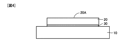
Fig. 4 is a schematic cross sectional view for illustrating the method for
manufacturing the silicon carbide substrate.
Fig. 5 is a schematic cross sectional view showing another structure of the
silicon carbide substrate.
Fig. 6 is a schematic plan view showing the another structure of the silicon
carbide substrate.
Fig. 7 is a schematic cross sectional view showing still another structure of
the
silicon carbide substrate.
Fig. 8 is a schematic cross sectional view showing a structure of a vertical
type
MOSFET.
Fig. 9 is a flowchart schematically showing a method for manufacturing the
vertical type MOSFET.
Fig. 10 is a schematic cross sectional view for illustrating the method for
manufacturing the vertical type MOSFET.
-15-
CA 02759861 2011-10-24 110277:910431
Fig. 1 1 is a schematic cross sectional view for illustrating the method for
manufacturing the vertical type MOSFET.
Fig. 12 is a schematic cross sectional view for illustrating the method for
manufacturing the vertical type MOSFET.
Fig. 13 is a schematic cross sectional view for illustrating the method for
manufacturing the vertical type MOSFET.
DESCRIPTION OF EMBODIMENTS
The following describes embodiments of the present invention with reference to
figures. It should be noted that in the below-mentioned figures, the same or
corresponding portions are given the same reference characters and are not
described
repeatedly.
(First Embodiment)
Referring to Fig. 1, silicon carbide substrate 1 in the present embodiment
includes: a base layer 10 made of silicon carbide; an intermediate layer 40
formed on
and in contact with base layer 10; and a SiC layer 20 made of single-crystal
silicon
carbide and disposed on and in contact with intermediate layer 40.
Intermediate layer
40 contains silicon carbide at least at its region adjacent to base layer 10
and its region
adjacent to SiC layer 20, and connects base layer 10 and SiC layer 20 to each
other.
The silicon carbide in each of the region adjacent to base layer 10 and the
region
adjacent to SiC layer 20 may be amorphous.
Then, when an epitaxial growth layer 60 made of single-crystal silicon carbide
is formed on main surface 20A of SiC layer 20 opposite to base layer 10 as
shown in
Fig. 2, stacking faults that can be generated in base layer 10 are not
propagated to
epitaxial growth layer 60. Accordingly, stacking fault density in epitaxial
growth layer
60 can be readily made smaller than that in base layer 10.
In silicon carbide substrate I in the present embodiment, SiC layer 20, which
is
made of single-crystal silicon carbide different from that of base layer 10,
is connected
onto base layer 10. Hence, for example, a low-quality silicon carbide crystal
having a
-16-
CA 02759861 2011-10-24 110277:910431
large defect density is processed to have a shape and a size suitable for the
process of
manufacturing a semiconductor device and is then employed as base layer 10. On
the
other hand, a high-quality silicon carbide single-crystal not having a shape
suitable for
the process of manufacturing a semiconductor device can be disposed on base
layer 10
as SiC layer 20. This silicon carbide substrate 1 is uniformly shaped and
sized
appropriately, thereby achieving efficient manufacturing of semiconductor
devices.
Further, because the high-quality silicon carbide single-crystal having a
difficulty in
being processed into a shape suitable for the process of manufacturing can be
used as
SiC layer 20 in silicon carbide substrate I to manufacture a semiconductor
device,
thereby effectively utilizing the silicon carbide single-crystal. Further, in
silicon
carbide substrate 1, base layer 10 and SiC layer 20 are unified by being
connected to
each other by intermediate layer 40 containing silicon carbide at its regions
adjacent to
base layer 10 and adjacent to SiC layer 20. Hence, silicon carbide substrate 1
can be
handled as one freestanding substrate. As such, silicon carbide substrate I
described
above allows for reduced cost in manufacturing semiconductor devices. Because
intermediate layer 40 thus includes silicon carbide at least at its regions
adjacent to base
layer 10 and adjacent to SiC layer 20, base layer 10 and SiC layer 20 are
connected to
each other more firmly.
Here, base layer 10 can adopt a structure from various structures as long as
it is
made of silicon carbide. For example, base layer 10 may be of, for example,
polycrystal silicon carbide or a sintered compact of silicon carbide.
Alternatively,
base layer 10 may be made of single-crystal silicon carbide. In this case, it
is
preferable that no micro pipes in base layer 10 are propagated to SiC layer
20. Further,
in the case where silicon carbide substrate I is employed to manufacture a
semiconductor device in which a current flows in the thickness direction of
silicon
carbide substrate 1, base layer 10 preferably has a small resistivity.
Specifically, base
layer 10 preferably has a resistivity of 50 mf2cm or smaller, more preferably,
10 mt2cm
or smaller.
-17-
CA 02759861 2011-10-24 110277:910431
In the case where single-crystal silicon carbide containing relatively many
defects such as micro pipes is employed as base layer 10, a high-quality
epitaxial
growth layer can be formed on SiC layer 20 by preventing the micro pipes
formed in
base layer 10 from being propagated to SiC layer 20. Silicon carbide substrate
1 in the
present embodiment can be fabricated by connecting SiC layer 20, which has not
been
grown on base layer 10 and has grown separately therefrom, onto base layer 10.
Hence, it is easy to prevent the micro pipes formed in base layer 10 from
being
propagated to SiC layer 20.
Further, in the case where base layer 10 is made of single-crystal silicon
carbide,
it is preferable that the main surface of base layer 10, which faces SiC layer
20 with
intermediate layer 40 interposed therebetween, has the same plane orientation
as that of
the main surface of SiC layer 20. This suppresses stress resulting from
anisotropy in
thermal expansion coefficient to exert between base layer 10 and SiC layer 20.
Further, in silicon carbide substrate 1 described above, main surface 20A of
SiC
substrate 20 opposite to base layer 10 may have an off angle of not less than
50 and
not more than 65 relative to the {0001 } plane. Accordingly, when fabricating
a
MOSFET using silicon carbide substrate 1, formation of interface states is
reduced
around an interface between an epitaxial growth layer and an oxide film
thereof, i.e., a
location where a channel region is formed. In this way, the MOSFET fabricated
has
reduced on-resistance.
Further, in silicon carbide substrate 1, the off orientation of main surface
20A
may form an angle of 5 or smaller relative to the <1-100> direction. The <1-
100>
direction is a representative off orientation in a silicon carbide substrate.
Variation in
the off orientation resulting from variation in a slicing process of the
process of
manufacturing the substrate is adapted to be 5 or smaller, which allows an
epitaxial
growth layer to be formed readily on silicon carbide substrate 1.
Further, in the silicon carbide substrate, main surface 20A may have an off
angle of not less than -3 and not more than 5 relative to the {03-38} plane
in the <1-
-18-
CA 02759861 2011-10-24 110277:910431
100> direction. Accordingly, channel mobility can be further improved in the
case
where a MOSFET is fabricated using silicon carbide substrate 1.
Meanwhile, in silicon carbide substrate 1, the off orientation of main surface
20A may form an angle of 5 or smaller relative to the <11-20> direction. The
<11-
20> direction is a representative off orientation in a silicon carbide
substrate, as with
the <1-100> direction. Variation in the off orientation resulting from
variation in a
slicing process of the process of manufacturing the substrate is adapted to be
5 ,
which allows an epitaxial growth layer to be formed readily on silicon carbide
substrate
1.
Further, in silicon carbide substrate 1, main surface 20A may have an off
angle
of not less than 1 0 and not more than 60 relative to the {0001 } plane. This
allows a
silicon carbide single-crystal usable as SiC layer 20 to be obtained
effectively, and
facilitates formation of a high-quality epitaxial growth layer on SiC layer
20.
Further, for ease of handling as a freestanding substrate, silicon carbide
substrate I preferably has a thickness of 300 m or greater. Further, when
silicon
carbide substrate 1 is employed to fabricate a power device, SiC layer 20
preferably has
a polytype of 4H.
Further, in silicon carbide substrate 1, main surface 20A of SiC layer 20
opposite to base layer 10 is preferably polished. This allows for formation of
a high-
quality epitaxial growth layer on main surface 20A. As a result, a
semiconductor
device can be manufactured which includes the high-quality epitaxial growth
layer as
an active layer, for example. Namely, by employing such a structure, silicon
carbide
substrate 1 can be obtained which allows for manufacturing of a high-quality
semiconductor device including the epitaxial layer formed on SiC layer 20.
The following describes an exemplary method for manufacturing silicon carbide
substrate 1 described above. Referring to Fig. 3, in the method for
manufacturing the
silicon carbide substrate in the present embodiment, first, as a step (S 10),
a substrate
preparing step is performed. In this step (S 10), referring to Fig. 4, a base
substrate 10
-19-
CA 02759861 2011-10-24 110277:910431
formed of silicon carbide and a SiC substrate 20 formed of single-crystal
silicon carbide
are prepared. SiC substrate 20 has the main surface, which will be main
surface 20A
of SiC layer 20 that will be obtained by this manufacturing method (see Fig.
1).
Hence, on this occasion, the plane orientation of the main surface of SiC
substrate 20 is
selected in accordance with desired plane orientation of main surface 20A.
Here, for
example, a SiC substrate 20 having a main surface corresponding to the {03-38}
plane
is prepared.
Meanwhile, for base substrate 10, a substrate having an impurity density
greater
than that of SiC substrate 20 is employed, such as a substrate having an
impurity
density greater than 2 x 10' 9 cm-3. Here, the term "impurity" refers to an
impurity
introduced to generate majority carriers in the semiconductor substrates,
i.e., base
substrate 10 and SiC substrate 20. A usable example thereof is nitrogen.
Further,
base substrate 10 preferably has a diameter of 2 inches or greater, more
preferably, of 6
inches or greater in order to achieve efficient fabrication of semiconductor
devices
using silicon carbide substrate 1. Further, in order to prevent generation of
cracks
between base substrate 10 and SiC substrate 20 in the process of manufacturing
semiconductor devices using silicon carbide substrate 1, it is preferable to
reduce a
difference in thermal expansion coefficient therebetween. Further, in order to
reduce a
difference between base substrate 10 and SiC substrate 20 in physical
properties such as
thermal expansion coefficient, base substrate 10 and SiC substrate 20
preferably have
the same crystal structure (the same polytype).
Next, a substrate smoothing step is performed as a step (S20). In this step
(S20), the respective main surfaces (connection surface) of base substrate 10
and SiC
substrate 20, which are to be disposed face to face with each other with a Si
film
interposed therebetween in a subsequent step (S40), are smoothed by polishing,
for
example. It should be noted that although this step (S20) is not an essential
step, by
performing this step, the Si film will be formed uniformly in a below-
described step
(S30) to allow base substrate 10 and SiC substrate 20 to be connected to each
other
-20-
CA 02759861 2011-10-24 110277:910431
more securely in a step (S50). Further, variation of the thickness of each of
base
substrate 10 and SiC substrate 20 (difference between the maximum value and
the
minimum value of the thickness) is preferably reduced as much as possible,
specifically,
is preferably 10 m or smaller.
Meanwhile, step (S20) may be omitted, i.e., step (S30) may be performed
without polishing the main surfaces of base substrate 10 and SiC substrate 20,
which
are to face each other. This reduces manufacturing cost of silicon carbide
substrate 1.
Further, for removal of damaged layers located in surfaces formed by slicing
upon
fabrication of base substrate 10 and SiC substrate 20, a step of removing the
damaged
layers may be performed by, for example, etching instead of step (S20) or
after step
(S20), and then step (S30) described below may be performed.
Next, a Si film forming step is performed as step (S30). In this step (S30),
referring to Fig. 4, Si film 30 made of silicon is formed on the main surface
of base
substrate 10. Si film 30 can be formed using a method such as a sputtering
method, a
deposition method, a liquid phase epitaxy, or a vapor phase epitaxy. Further,
in
forming Si film 30, nitrogen, phosphorus, aluminum, boron, or the like can be
doped as
an impurity. Further, Si film 30 may be adapted to contain titanium to improve
solid
solubility of carbon in Si film 30 to facilitate conversion thereof into
silicon carbide in
the below-described step (S50).
Next, a stacking step is performed as step (S40). In this step (S40),
referring to
Fig. 4, SiC substrate 20 is placed on and in contact with Si film 30 formed on
and in
contact with the main surface of base substrate 10, thereby fabricating a
stacked
substrate.
Next, as step (S50), a connecting step is performed. In step (S50), base
substrate 10 and SiC substrate 20 are connected to each other by heating the
stacked
substrate. More specifically, for example, the stacked substrate is heated for
not less
than 1 hour and not more than 30 hours to fall within a range of temperature
from
1300 C to 1 800 C. In this way, carbon is supplied from base substrate 10 and
SiC
-21-
= f CA 02759861 2011-10-24 110277:910431
substrate 20 to Si film 30, thereby converting at least portions of Si film 30
into silicon
carbide. By performing the heating under a gas containing carbon atoms, for
example,
under an atmosphere including a hydrocarbon gas such as propane, ethane, or
ethylene,
carbon is supplied from the atmosphere to Si film 30 to facilitate the
conversion of
silicon constituting Si film 30 into silicon carbide. By heating the stacked
substrate in
this way, at least the region in contact with base substrate 10 and the region
in contact
with SiC substrate 20 in Si film 30 are converted into silicon carbide,
thereby
connecting base substrate 10 and SiC substrate 20 to each other. As a result,
silicon
carbide substrate I shown in Fig. I is obtained. Further, the atmosphere upon
the
heating in step (S50) may be inert gas atmosphere. In the case where the
atmosphere
is the inert gas atmosphere, the inert gas atmosphere preferably contains at
least one
selected from a group consisting of argon, helium, and nitrogen. Further, in
this step
(S50), the stacked substrate may be heated in an atmosphere obtained by
reducing
pressure of the atmospheric air. This reduces manufacturing cost of silicon
carbide
substrate 1.
Thus, in the method for manufacturing silicon carbide substrate I in the
present
embodiment, SiC substrate 20 made of single-crystal silicon carbide different
from that
of base substrate 10 is connected onto base substrate 10. As such, base
substrate 10
formed of an inexpensive, low-quality silicon carbide crystal having a large
defect
density can be processed to have a shape and a size suitable for manufacturing
of
semiconductor devices, whereas a high-quality silicon carbide single-crystal
not having
a shape and the like suitable for manufacturing of semiconductor devices can
be
disposed as SiC substrate 20 on base substrate 10. Silicon carbide substrate I
manufactured through such a process has the predetermined uniform shape and
size.
This allows for efficient manufacturing of semiconductor devices. Further,
silicon
carbide substrate 1 manufactured through such a process utilizes such a high-
quality
SiC substrate 20 (SiC layer 20) to manufacture a semiconductor device, thereby
effectively utilizing silicon carbide single-crystal. Further, in the method
for
-22-
CA 02759861 2011-10-24 110277:910431
manufacturing silicon carbide substrate 1 in the present invention, base
substrate 10 and
SiC substrate 20 are firmly connected to each other by intermediate layer 40
formed by
converting at least the portions of Si film 30 into silicon carbide. Hence,
silicon
carbide substrate 1 can be handled as one freestanding substrate. As such,
according
to the method for manufacturing silicon carbide substrate 1 in the present
embodiment,
there can be manufactured a silicon carbide substrate I that allows for
reduced cost of
manufacturing semiconductor devices using silicon carbide substrate 1.
Further, by epitaxially growing single-crystal silicon carbide on silicon
carbide
substrate 1 to form an epitaxial growth layer 60 on main surface 20A of SiC
substrate
20, a silicon carbide substrate 2 shown in Fig. 2 can be manufactured.
Here, in step (S30), the Si film formed preferably has a thickness of not less
than 10 nm and not more than 1 m. If the thickness of Si film 30 formed on
base
substrate 10 is less than 10 nm and surface smoothness of each of the surfaces
of base
substrate 10 and SiC substrate 20 is not sufficiently high, Si film 30 to be
formed
between base substrate 10 and SiC substrate 20 becomes discontinuous, which
may
lead to failure in achieving firm connection between base substrate 10 and SiC
substrate
20. In contrast, if the thickness of Si film 30 is more than I m, the
thickness of
intermediate layer 40 in the thickness of silicon carbide substrate I becomes
large.
This may result in decreased characteristics particularly when fabricating a
vertical type
device in which a current flows in the thickness direction of silicon carbide
substrate 1.
Thus, Si film 30 formed preferably has a thickness of not less than 10 nm and
not more
than 1 m.
Further, in step (S40), the stacked substrate is preferably fabricated such
that the
plane orientations of the main surfaces of base substrate 10 and SiC substrate
20, which
face each other with Si film 30 interposed therebetween, coincide with each
other.
This suppresses stress resulting from anisotropy in thermal expansion
coefficient to
exert between base substrate 10 and SiC substrate 20.
Further, in step (S50), Si film 30 (intermediate layer 40) may be doped with a
- 23 -
CA 02759861 2011-10-24 110277:910431
desired impurity by adding nitrogen, trimethylaluminum, diborane, phosphine,
or the
like in the atmosphere in which the stacked substrate is heated.
In the above-described embodiment, it has been illustrated that: in the
stacked
substrate fabricated in step (S40), main surface 20A of SiC substrate 20
opposite to
base substrate 10 has an off orientation corresponding to the <1-100>
direction, and
main surface 20A thereof corresponds to the {03-38} plane. However, instead of
this,
the main surface may have an off orientation forming an angle of 5 or smaller
relative
to the <11-20> direction. Further, main surface 20A may have an off angle of
not less
than 1 and not more than 60 relative to the {0001 } plane.
Further, the above-described method for manufacturing silicon carbide
substrate
1 in the present embodiment may further include a step of polishing the main
surface of
SiC substrate 20 that corresponds to main surface 20A of SiC substrate 20
opposite to
base substrate 10 in the stacked substrate. Accordingly, a silicon carbide
substrate I is
manufactured in which main surface 20A of SiC layer 20 opposite to base layer
10 has
been polished. Here, the step of polishing may be performed before or after
connecting base substrate 10 and SiC substrate 20 to each other, as long as
the step of
polishing is performed after step (S 10).
(Second Embodiment)
The following describes another embodiment of the present invention, i.e., a
second embodiment. Referring to Fig. 5, Fig. 6, and Fig. 1, a silicon carbide
substrate
I in the second embodiment has basically the same configuration and provides
basically
the same effects as those of silicon carbide substrate 1 in the first
embodiment.
However, silicon carbide substrate 1 in the second embodiment is different
from that of
the first embodiment in that a plurality of SiC layers 20 are arranged side by
side when
viewed in a planar view.
Namely, referring to Fig. 5 and Fig. 6, in silicon carbide substrate 1 of the
second embodiment, the plurality of SiC layers 20 are arranged side by side
when
viewed in a planar view. In other words, the plurality of SiC layers 20 are
arranged
-24-
' = ' CA 02759861 2011-10-24 110277:910431
along main surface IOA of base layer 10. More specifically, the plurality of
SiC layers
20 are arranged in the form of a matrix on base layer 10 such that adjacent
SiC layers
20 are in contact with each other. Accordingly, silicon carbide substrate I of
the
present embodiment can be handled as a substrate having high-quality SiC
layers 20
and a large diameter. Utilization of such a silicon carbide substrate 1 allows
for
efficient manufacturing process of semiconductor devices. It should be noted
that
silicon carbide substrate I in the second embodiment can be manufactured in a
similar
way to that in the first embodiment by arranging the plurality of SiC
substrates 20 side
by side on Si film 30 in step (S40) in the first embodiment. It should be
noted that
there may be formed a space between adjacent SiC layers (SiC substrates) 20.
The
space is preferably 100 m or smaller, more preferably, 10 m or smaller.
Further, in the second embodiment, it has been illustrated that the plurality
of
SiC layers 20 each having a planar shape of square (quadrangle) are disposed
on base
layer 10, but the shape of each of SiC layers 20 is not limited to this.
Specifically,
referring to Fig. 7, the planar shapes of SiC layers 20 can be any shapes such
as a
hexagon shape, a trapezoidal shape, a rectangular shape, and a circular shape,
or may be
a combination thereof.
(Third Embodiment)
As a third embodiment, the following describes one exemplary semiconductor
device fabricated using the above-described silicon carbide substrate of the
present
invention. Referring to Fig. 8, a semiconductor device 101 according to the
present
invention is a DiMOSFET (Double Implanted MOSFET) of vertical type, and has a
substrate 102, a buffer layer 121, a breakdown voltage holding layer 122, p
regions 123,
n+ regions 124, p+ regions 125, an oxide film 126, source electrodes 111,
upper source
electrodes 127, a gate electrode 110, and a drain electrode 112 formed on the
backside
surface of substrate 102. Specifically, buffer layer 121 made of silicon
carbide is
formed on the front-side surface of substrate 102 made of silicon carbide of n
type
conductivity. Employed as substrate 102 is a silicon carbide substrate of the
present
- 25 -
CA 02759861 2011-10-24 110277:910431
invention, inclusive of silicon carbide substrate I described in each of the
first and
second embodiments. In the case where silicon carbide substrate 1 in each of
the first
and second embodiments is employed, buffer layer 121 is formed on SiC layer 20
of
silicon carbide substrate 1. Buffer layer 121 has n type conductivity, and has
a
thickness of, for example, 0,5 m. Further, impurity with n type conductivity
in buffer
layer 121 has a density of, for example, 5 x 1017 cm-3. Formed on buffer layer
121 is
breakdown voltage holding layer 122. Breakdown voltage holding layer 122 is
made
of silicon carbide of n type conductivity, and has a thickness of 10 m, for
example.
Further, breakdown voltage holding layer 122 includes an impurity of n type
conductivity at a density of, for example, 5 X 1015 cm-3.
Breakdown voltage holding layer 122 has a surface in which p regions 123 of p
type conductivity are formed with a space therebetween. In each of p regions
123, an
n+ region 124 is formed at the surface layer of p region 123. Further, at a
location
adjacent to n+ region 124, a p+ region 125 is formed. Oxide film 126 is formed
to
extend on n+ region 124 in one p region 123, p region 123, an exposed portion
of
breakdown voltage holding layer 122 between the two p regions 123, the other p
region
123, and n+ region 124 in the other p region 123. On oxide film 126, gate
electrode
110 is formed. Further, source electrodes 11 1 are formed on n+ regions 124
and p+
regions 125. On source electrodes 111, upper source electrodes 127 are formed.
Moreover, drain electrode 112 is formed on the backside surface of substrate
102, i.e.,
the surface opposite to its front-side surface on which buffer layer 121 is
formed.
Employed as substrate 102 in semiconductor device 101 of the present
embodiment is a silicon carbide substrate of the present invention such as
silicon
carbide substrate 1 described above in the first and second embodiments. Here,
as
described above, the silicon carbide substrate of the present invention allows
for
reduced manufacturing cost of semiconductor devices. Hence, semiconductor
device
101 is manufactured with the reduced manufacturing cost.
The following describes a method for manufacturing semiconductor device 101
-26-
CA 02759861 2011-10-24 110277:910431
shown in Fig. 8, with reference to Fig. 9-Fig. 13. Referring to Fig. 9, first,
a substrate
preparing step (S 110) is performed. Prepared here is, for example, substrate
102,
which is made of silicon carbide and has its main surface corresponding to the
(03-38).
plane (see Fig. 10). As substrate 102, there is prepared a silicon carbide
substrate of
the present invention, inclusive of silicon carbide substrate I manufactured
in
accordance with each of the manufacturing methods described in the first and
second
embodiments.
Alternatively, as substrate 102 (see Fig. 10), a substrate may be employed
which
has n type conductivity and has a substrate resistance of 0.02 acm.
Next, as shown in Fig. 9, an epitaxial layer forming step (S120) is performed.
Specifically, buffer layer 121 is formed on the front-side surface of
substrate 102.
Buffer layer 121 is formed on SiC layer 20 (see Fig. 1 and Fig. 5) of silicon
carbide
substrate 1 employed as substrate 102. As buffer layer 121, an epitaxial layer
is
formed which is made of silicon carbide of n type conductivity and has a
thickness of
0.5 m, for example. Buffer layer 121 has a conductive impurity at a density
of, for
example, 5 x 1017 cm"3. Then, on buffer layer 121, breakdown voltage holding
layer
122 is formed as shown in Fig. 10. As breakdown voltage holding layer 122, a
layer
made of silicon carbide of n type conductivity is formed using an epitaxial
growth
method. Breakdown voltage holding layer 122 can have a thickness of, for
example,
10 m. Further, breakdown voltage holding layer 122 includes an impurity of n
type
conductivity at a density of, for example, 5 x 1015 cm-3.
Next, as shown in Fig. 9, an implantation step (S130) is performed.
Specifically, an impurity of p type conductivity is implanted into breakdown
voltage
holding layer 122 using, as a mask, an oxide film formed through
photolithography and
etching, thereby forming p regions 123 as shown in Fig. 11. Further, after
removing
the oxide film thus used, an oxide film having a new pattern is formed through
photolithography and etching. Using this oxide film as a mask, a conductive
impurity
of n type conductivity is implanted into predetermined regions to form n+
regions 124.
-27-
CA 02759861 2011-10-24 110277:910431
In a similar way, a conductive impurity of p type conductivity is implanted to
form p+
regions 125. As a result, the structure shown in Fig. 11 is obtained.
After such an implantation step, an activation annealing process is performed.
This activation annealing process can be performed under conditions that, for
example,
argon gas is employed as atmospheric gas, heating temperature is set at 1700
C, and
heating time is set at 30 minutes.
Next, a gate insulating film forming step (S 140) is performed as shown in
Fig. 9.
Specifically, as shown in Fig. 12, oxide film 126 is formed to cover breakdown
voltage
holding layer 122, p regions 123, n+ regions 124, and p regions 125. As a
condition
for forming oxide film 126, for example, dry oxidation (thermal oxidation) may
be
performed. The dry oxidation can be performed under conditions that the
heating
temperature is set at 1200 C and the heating time is set at 30 minutes.
Thereafter, a nitrogen annealing step (S 150) is performed as shown in Fig. 9.
Specifically, an annealing process is performed in atmospheric gas of nitrogen
monoxide (NO). Temperature conditions for this annealing process are, for
example,
as follows: the heating temperature is 1100 C and the heating time is 120
minutes. As
a result, nitrogen atoms are introduced into a vicinity of the interface
between oxide
film 126 and each of breakdown voltage holding layer 122, p regions 123, n+
regions
124, and p+ regions 125, which are disposed below oxide film 126. Further,
after the
annealing step using the atmospheric gas of nitrogen monoxide, additional
annealing
may be performed using argon (Ar) gas, which is an inert gas. Specifically,
using the
atmospheric gas of argon gas, the additional annealing may be performed under
conditions that the heating temperature is set at 1 100 C and the heating time
is set at 60
minutes.
Next, as shown in Fig. 9, an electrode forming step (S 160) is performed.
Specifically, a resist film having a pattern is formed on oxide film 126 by
means of the
photolithography method. Using the resist film as a mask, portions of the
oxide film
above n+ regions 124 and p+ regions 125 are removed by etching. Thereafter, a
-28-
CA 02759861 2011-10-24 110277:910431
conductive film such as a metal is formed on the resist film and formed in
openings of
oxide film 126 in contact with n+ regions 124 and p+ regions 125. Thereafter,
the
resist film is removed, thus removing the conductive film's portions located
on the
resist film (lift-off). Here, as the conductor, nickel (Ni) can be used, for
example.
As a result, as shown in Fig. 13, source electrodes Ill and drain electrode
112 can be
obtained. It should be noted that on this occasion, heat treatment for
alloying is
preferably performed. Specifically, using atmospheric gas of argon (Ar) gas,
which is
an inert gas, the heat treatment (alloying treatment) is performed with the
heating
temperature being set at 950 C and the heating time being set at 2 minutes.
Thereafter, on source electrodes 111, upper source electrodes 127 (see Fig. 8)
are formed. Further, drain electrode 112 is formed on the backside surface of
substrate 102 (see Fig. 8). Further, gate electrode 110 (see Fig. 8) is formed
on oxide
film 126. In this way, semiconductor device 101 shown in Fig. 8 can be
obtained.
Namely, semiconductor device 101 is fabricated by forming the epitaxial layer
and the
electrodes on SiC layer 20 of silicon carbide substrate 1.
It should be noted that in the third embodiment, the vertical type MOSFET has
been illustrated as one exemplary semiconductor device that can be fabricated
using the
silicon carbide substrate of the present invention, but the semiconductor
device that can
be fabricated is not limited to this. For example, various types of
semiconductor
devices can be fabricated using the silicon carbide substrate of the present
invention,
such as a JFET (Junction Field Effect Transistor), an IGBT (Insulated Gate
Bipolar
Transistor), and a Schottky barrier diode. Further, the third embodiment has
illustrated a case where the semiconductor device is fabricated by forming the
epitaxial
layer, which serves as an active layer, on the silicon carbide substrate
having its main
surface corresponding to the (03-38) plane. However, the crystal plane that
can be
adopted for the main surface is not limited to this and any crystal plane
suitable for the
purpose of use and including the (0001) plane can be adopted for the main
surface.
[Example]
-29-
74 CA 02759861 2011-10-24 110277:910431
The following describes an example of the present invention. An experiment
was conducted to inspect electric characteristics in the intermediate layer
(connection
interface) of an actually fabricated silicon carbide substrate of the present
invention.
The experiment was conducted in the following manner.
First, a silicon carbide substrate of the present invention was fabricated as
a
sample. The silicon carbide substrate was fabricated in the same manner as in
the first
embodiment. Specifically, a base substrate and a SiC substrate were prepared.
Employed as the base substrate was a substrate having a shape with a diameter
4) of 4
inches and a thickness of 300 m, made of single-crystal silicon carbide with
polytype
of 4H, and having a main surface corresponding to the (03-38) plane. Further,
the
base substrate had n type conductivity, and had an n type impurity density of
I X 1020
cm-3. Further, the base substrate had a micro pipe density of I X 104 em"2,
and had a
stacking fault density of I X 105 cm-1.
Employed as the SiC substrate was a substrate having a planar shape of square
with each side of 20 mm, having a thickness of 300 m, made of single-crystal
silicon
carbide with a polytype of 4H, and having a main surface corresponding to the
(03-38)
plane. Further, the SiC substrate had n type conductivity, and had an n type
impurity
density of 1 X 10' 9 em-3. Further, the SiC substrate had a micro pipe density
of 0.2 cm-
2 and had a stacking fault density less than 1 cm-1.
Next, on the base substrate, a Si film having a thickness of 100 nm was formed
using the sputtering method. Thereafter, the SiC substrate was placed on the
Si film to
fabricate a stacked substrate. Then, this stacked substrate was heated at 1500
C for 3
hours, thereby converting at least portions of the Si film into silicon
carbide to connect
the base substrate and the SiC substrate to each other. The atmosphere during
the
heating was a mixed gas of hydrogen gas and propane, and has a pressure of 1 x
103 Pa.
Further, the flow rate of the hydrogen gas was set at 3 slm, and the flow rate
of propane
was set at 80 sccm. It should be noted that the flow rate of the hydrogen gas
can be set
at 1 to 10 slm, and the flow rate of propane can be set at 50 to 500 seem.
With the
-30-
CA 02759861 2011-10-24 110277:910431
above-described procedure, the silicon carbide substrate serving as the sample
was
fabricated.
Next, the main surface of the silicon carbide substrate obtained was polished
to
achieve a uniform thickness, whereby variation of the thickness (difference
between the
maximum value and the minimum value of the thickness of the silicon carbide
substrate) became 5 m. Further, ohmic electrodes were formed on both the main
surfaces of the silicon carbide substrate. The ohmic electrodes were formed by
forming nickel films on the main surfaces thereof and heating them for
silicidation.
The heat treatment for silicidation can be performed by heating them in an
inert gas
atmosphere to a temperature of not less than 900 C and not more than 1 100 C
for not
less than 10 minutes and not more than 10 hours. In this experiment, the heat
treatment was performed by heating them in an argon atmosphere under an
atmospheric
pressure to 1000 C for 1 hour. Then, a voltage was applied between the ohmic
electrodes to inspect electric characteristics of the connection interface
(intermediate
layer formed by converting at least portions of the Si film into silicon
carbide).
As a result, it was confirmed that ohmic characteristics were obtained in the
connection interface. From this, it was confirmed that according to the method
for
manufacturing the silicon carbide substrate of the present invention, the
plurality of
substrates made of silicon carbide can be connected to each other while
securing ohmic
characteristics in the thickness direction thereof.
The silicon carbide substrate of the present invention can be used to
fabricate a
semiconductor device as described above in the third embodiment. Namely, in
the
semiconductor device of the present invention, the epitaxial growth layer is
formed as
an active layer on the silicon carbide substrate manufactured using the method
for
manufacturing the silicon carbide substrate in the present invention.
Explaining from
a different point of view, in the semiconductor device of the present
invention, the
epitaxial growth layer is formed on the silicon carbide substrate of the
present invention
as an active layer. More specifically, the semiconductor device of the present
-31-
CA 02759861 2011-10-24 110277:910431
invention includes: the silicon carbide substrate of the present invention;
the epitaxial
growth layer formed on the silicon carbide substrate; and the electrodes
formed on the
epitaxial growth layer. Namely, the semiconductor device of the present
invention
includes: the base layer made of silicon carbide; the intermediate layer
formed on and in
contact with the base layer; the SiC layer made of single-crystal silicon
carbide and
disposed on and in contact with the intermediate layer; the epitaxial growth
layer
formed on the SiC layer; and the electrodes formed on the epitaxial growth
layer. In
addition, the intermediate layer contains silicon carbide at least at its
region adjacent to
the base layer and its region adjacent to the SiC layer, and connects the base
layer and
the SiC layer to each other.
The embodiments and example disclosed herein are illustrative and non-
restrictive in any respect. The scope of the present invention is defined by
the terms of
the claims, rather than the embodiments described above, and is intended to
include any
modifications within the scope and meaning equivalent to the terms of the
claims.
INDUSTRIAL APPLICABILITY
A method for manufacturing a silicon carbide substrate, and the silicon
carbide
substrate in the present invention are particularly advantageously applicable
to a
method for manufacturing a silicon carbide substrate, and the silicon carbide
substrate,
each of which achieves reduced cost of manufacturing a semiconductor device
using
the silicon carbide substrate.
REFERENCE SIGNS LIST
1, 2: silicon carbide substrate; 10: base layer (base substrate); 20: SiC
layer (SiC
substrate); 20A: main surface; 30: Si film; 40: intermediate layer; 101:
semiconductor
device; 102: substrate; 110: gate electrode; I11: source electrode; 112: drain
electrode;
121: buffer layer; 122: breakdown voltage holding layer; 123: p region; 124:
n+ region;
1,25: p+ region; 126: oxide film; 127: upper source electrode.
-32-