Note: Descriptions are shown in the official language in which they were submitted.
CA 02761428 2011-11-08 110034 : 910089
DESCRIPTION
TITLE OF INVENTION
Silicon Carbide Substrate, Semiconductor Device, and Method of
Manufacturing Silicon Carbide Substrate
TECHNICAL FIELD
The present invention relates to a silicon carbide substrate, a semiconductor
device, and a method of manufacturing a silicon carbide substrate, and more
particularly to a silicon carbide substrate allowing reduction in cost for
manufacturing a
semiconductor device including a silicon carbide substrate and a method of
manufacturing the same, as well as a semiconductor device of which
manufacturing
cost has been reduced.
BACKGROUND ART
In recent years, in order to achieve a higher breakdown voltage and lower loss
of
a semiconductor device, use thereof in an environment at high temperature and
the like,
silicon carbide has increasingly been adopted as a material for a
semiconductor device.
Silicon carbide is a wide band-gap semiconductor greater in band gap than
silicon
conventionally widely used as a material for a semiconductor device.
Therefore, by
adopting silicon carbide as a material for a semiconductor device, a higher
breakdown
voltage, a lower ON resistance of a semiconductor device and the like can be
achieved.
In addition, a semiconductor device adopting silicon carbide as a material is
also more
advantageous than a semiconductor device adopting silicon as a material in
that
deterioration in its characteristics at the time when it is used in an
environment at high
temperature is less.
Under such circumstances, various studies have been conducted on a method of
manufacturing silicon carbide crystal and a silicon carbide substrate used for
manufacturing a semiconductor device, and various ideas have been proposed
(see, for
example, M. Nakabayashi et al., "Growth of Crack-free 100 mm-diameter 4H-SiC
- I -
i
CA 02761428 2011-11-08 110034:910089
Crystals with Low Micropipe Densities," Mater. Sci. Forum, vols. 600-603,
2009, pp.
3-6 (NPL 1)).
CITATION LIST
NON PATENT LITERATURE
NPL 1: M. Nakabayashi et al., "Growth of Crack-free 100 mm-diameter 4H-SiC
Crystals with Low Micropipe Densities," Mater. Sci. Forum, vols. 600-603,
2009, pp.
3-6
SUMMARY OF INVENTION
TECHNICAL PROBLEM
Silicon carbide, however, is not in a liquid phase at a normal pressure. In
addition, a crystal growth temperature is very high, i.e., 2000 C or higher,
and control
of a growth condition or stable control is difficult. Therefore, it is
difficult to obtain
large-diameter silicon carbide single crystal while maintaining high quality,
and it is not
easy to obtain a high-quality silicon carbide substrate having a large
diameter. Owing
to difficulty in fabrication of a silicon carbide substrate having a large
diameter, not
only cost for manufacturing a silicon carbide substrate increases but also the
number of
products per one batch is small in manufacturing semiconductor devices
including the
silicon carbide substrates, and hence cost for manufacturing semiconductor
devices
increases. By making effective use of silicon carbide single crystal high in
manufacturing cost as a substrate, it is expected that cost for manufacturing
a
semiconductor device can be reduced.
An object of the present invention is to provide a silicon carbide substrate
allowing reduction in cost for manufacturing a semiconductor device including
a silicon
carbide substrate and a method of manufacturing the same, as well as a
semiconductor
device of which manufacturing cost has been reduced.
SOLUTION TO PROBLEM
A silicon carbide substrate according to the present invention includes a base
substrate composed of silicon carbide and an SiC layer composed of single
crystal
-2-
CA 02761428 2011-11-08 110034:910089
silicon carbide different from the base substrate and arranged on the base
substrate in
contact therewith.
As described above, it is difficult to obtain large-diameter silicon carbide
single
crystal of high quality. On the other hand, for efficient manufacturing in a
process for
manufacturing semiconductor devices each including a silicon carbide
substrate,
substrates uniform in prescribed shape and size are required. Therefore, even
when
silicon carbide single crystal of high quality (for example, silicon carbide
single crystal
low in fault density) is obtained, effective use of a region that cannot be
worked to a
prescribed shape or the like by cutting or the like may not be made.
In contrast, in the silicon carbide substrate according to the present
invention, an
SiC layer composed of single crystal silicon carbide different from the base
substrate is
arranged on the base substrate. Therefore, for example, a base substrate
composed of
silicon carbide crystal high in fault density and low in quality can be worked
to the
prescribed shape and size above so that silicon carbide single crystal not
having a
desired shape or the like although having high quality can be arranged on the
base
substrate as an SiC layer. Such silicon carbide substrates are uniform in
prescribed
shape and size, and thus more efficient manufacturing of semiconductor devices
can be
achieved. In addition, since semiconductor devices can be manufactured with
the use
of high-quality SiC layers for such silicon carbide substrates, effective use
of silicon
carbide single crystal can be made. Consequently, according to the silicon
carbide
substrate in the present invention, a silicon carbide substrate allowing
reduction in cost
for manufacturing a semiconductor device including a silicon carbide substrate
can be
provided. Here, such a state that the SiC layer above is composed of single
crystal
silicon carbide different from the base substrate includes a case where the
base
substrate is composed of silicon carbide other than single crystal, such as
polycrystalline and amorphous silicon carbide, and a case where the base
substrate is
composed of single crystal silicon carbide and made of crystal different from
the SiC
layer. A state in which the base substrate and the SiC layer are composed of
crystals
-3-
i
CA 02761428 2011-11-08 110034 : 910089
different from each other means a state that a boundary is present between the
base
substrate and the SiC layer, and for example, fault density is different
between one side
and the other side of the boundary. Here, fault density may be discontinuous
at the
boundary.
In the silicon carbide substrate above, preferably, the base substrate is
composed
of single crystal silicon carbide. The SiC layer is lower in micropipe density
than the
base substrate.
In addition, in the silicon carbide substrate above, preferably, the base
substrate
is composed of single crystal silicon carbide. The SiC layer is preferably
lower in
dislocation density than the base substrate. More specifically, in the silicon
carbide
substrate above, preferably, the base substrate is composed of single crystal
silicon
carbide. Then, the SiC layer is lower in threading screw dislocation density
than the
base substrate.
In addition, in the silicon carbide substrate above, preferably, the base
substrate
is composed of single crystal silicon carbide. The SiC layer is lower in
threading edge
dislocation density than the base substrate.
In addition, in the silicon carbide substrate above, preferably, the base
substrate
is composed of single crystal silicon carbide. The SiC layer is lower in basal
plane
dislocation density than the base substrate.
In addition, in the silicon carbide substrate above, preferably, the base
substrate
is composed of single crystal silicon carbide. The SiC layer is lower in
composite
dislocation density than the base substrate.
In addition, in the silicon carbide substrate above, preferably, the base
substrate
is composed of single crystal silicon carbide. The SiC layer is lower in
stacking fault
density than the base substrate.
In addition, in the silicon carbide substrate above, preferably, the base
substrate
is composed of single crystal silicon carbide. The SiC layer is lower in point
defect
density than the base substrate.
-4-
i
CA 02761428 2011-11-08 110034:910089
As described above, a silicon carbide substrate allowing manufacturing of a
semiconductor device of high quality can be obtained by arranging an SiC layer
lower
than the base substrate in fault density such as micropipe density,
dislocation density
(threading screw dislocation density, threading edge dislocation density,
basal plane
dislocation density, composite dislocation density, stacking fault density,
point defect
density), or the like.
In the silicon carbide substrate above, preferably, the base substrate is
composed
of single crystal silicon carbide. The SiC layer is smaller in a full width at
half
maximum of X-ray rocking curve than the base substrate. Thus, a silicon
carbide
substrate allowing manufacturing of a semiconductor device of high quality can
be
obtained by arranging an SiC layer smaller in a full width at half maximum of
X-ray
rocking curve, that is, higher in crystallinity, than the base substrate.
In the silicon carbide substrate above, the base substrate may include a
single
crystal layer composed of single crystal silicon carbide so as to include a
main surface
on a side facing the SiC layer. By doing so, in manufacturing a semiconductor
device
including a silicon carbide substrate, such a state of a large thickness as
readily being
handled is maintained in an early stage of a manufacturing process, and during
the
manufacturing process, a region of the base substrate other than a single
crystal layer is
removed to allow only the single crystal layer of the base substrate to remain
in the
inside of the semiconductor device. Thus, a semiconductor device of high
quality can
be manufactured while handling of a silicon carbide substrate in the
manufacturing
process is facilitated.
In the silicon carbide substrate above, preferably, the SiC layer is lower in
micropipe density than the single crystal layer above.
In addition, in the silicon carbide substrate above, preferably, the SiC layer
is
lower in dislocation density than the single crystal layer above. More
specifically, in
the silicon carbide substrate above, preferably, the SiC layer is lower in
threading screw
dislocation density than the single crystal layer above.
-5-
i
CA 02761428 2011-11-08 110034;910089
In addition, in the silicon carbide substrate above, preferably, the SiC layer
is
lower in threading edge dislocation density than the single crystal layer
above.
In addition, in the silicon carbide substrate above, preferably, the SiC layer
is
lower in basal plane dislocation density than the single crystal layer above.
In addition, in the silicon carbide substrate above, preferably, the SiC layer
is
lower in composite dislocation density than the single crystal layer above.
In addition, in the silicon carbide substrate above, preferably, the SiC layer
is
lower in stacking fault density than the single crystal layer above.
In addition, in the silicon carbide substrate above, preferably, the SiC layer
is
lower in point defect density than the single crystal layer above.
Thus, a silicon carbide substrate allowing manufacturing of a semiconductor
device of high quality can be obtained by arranging an SiC layer lower than
the single
crystal layer of the base substrate in fault density such as micropipe
density, dislocation
density (threading screw dislocation density, threading edge dislocation
density, basal
plane dislocation density, composite dislocation density, stacking fault
density, point
defect density), or the like.
In the silicon carbide substrate above, preferably, the SiC layer is smaller
in a
full width at half maximum of X-ray rocking curve than the single crystal
layer above.
Thus, a silicon carbide substrate allowing manufacturing of a semiconductor
device of
high quality can be obtained by arranging an SiC layer smaller in a full width
at half
maximum of X-ray rocking curve, that is, higher in crystallinity, than the
single crystal
layer of the base substrate.
In the silicon carbide substrate above, impurity density in the base substrate
can
be not lower than 5x 1018 cm-3. Thus, carrier density in the base substrate
increases so
that a silicon carbide substrate suitable for manufacturing, for example, a
vertical
semiconductor device in which an electrode is formed on a main surface of the
base
substrate opposite to the side where the SiC layer is formed and a current
path crosses
the base substrate in a direction of thickness, can be obtained.
-6-
i
CA 02761428 2011-11-08 110034:910089
In the silicon carbide substrate above, the base substrate can have
resistivity not
lower than lx 105 Qcm. Thus, a resistance value of the base substrate
increases, and a
silicon carbide substrate suitable for manufacturing, for example, a
semiconductor
device which is a lateral semiconductor device in which a current flows in a
direction
along a main surface of the base substrate and is required to adapt to a
higher frequency
can be obtained.
In the silicon carbide substrate above, a plurality of SiC layers above may be
stacked. Thus, a silicon carbide substrate including SiC layers in accordance
with an
intended structure of a semiconductor device can be obtained.
In the silicon carbide substrate above, preferably, a plurality of SiC layers
are
two-dimensionally arranged in alignment. Giving the description from a
different
point of view, a plurality of SiC layers are preferably arranged in alignment
along a
main surface of the base substrate. As described above, it is difficult to
obtain large-
diameter silicon carbide single crystal of high quality. In contrast, a
plurality of SiC
layers taken from silicon carbide single crystal of high quality are two-
dimensionally
arranged in alignment on the base substrate of a large diameter, so that a
silicon carbide
substrate that can be handled as a large-diameter substrate having SiC layers
of high
quality can be obtained. Then, by using this silicon carbide substrate,
efficiency in a
process for manufacturing a semiconductor device can be improved. In order to
improve efficiency in a process for manufacturing a semiconductor device, SiC
layers
adjacent to each other among the plurality of SiC layers above are preferably
arranged
in contact with each other. More specifically, for example, the plurality of
SiC layers
above are preferably two-dimensionally paved in matrix. In addition, end
surfaces of
respective adjacent SiC layers are preferably substantially perpendicular to
the main
surface of the SiC layer. Thus, a silicon carbide substrate can readily be
manufactured.
Here, it can be determined that the end surface above is substantially
perpendicular to
the main surface, for example, if an angle between the end surface above and
the main
surface is not smaller than 85 and not greater than 95 .
-7-
CA 02761428 2011-11-08 110034 : 910089
In the silicon carbide substrate above, a main surface of the SiC layer
opposite
to the base substrate has an off angle with respect to a plane orientation
{0001 } not
smaller than 50 and not greater than 65 .
Hexagonal silicon carbide single crystal is grown in a <0001> direction, so
that
single crystal of high quality can efficiently be fabricated. Then, a silicon
carbide
substrate having a {0001 } plane as the main surface can efficiently be taken
from
silicon carbide single crystal grown in the <0001> direction. Meanwhile, in
some
cases, a semiconductor device of high performance can be manufactured with a
silicon
carbide substrate including a main surface having an off angle with respect to
plane
orientation {0001 } not smaller than 50 and not greater than 65 , such as a
main surface
having a plane orientation {03-38}. When a silicon carbide substrate including
a main
surface having an off angle with respect to plane orientation {0001 } not
smaller than
50 and not greater than 65 is taken from silicon carbide single crystal
grown in the
<0001> direction, however, effective use of many portions in silicon carbide
single
crystal is not made.
In contrast, according to the silicon carbide substrate in the present
invention
above, since silicon carbide single crystal indefinite in shape can be used as
an SiC
layer, effective use of silicon carbide single crystal can be made even though
the main
surface of the SiC layer has an off angle with respect to plane orientation
{0001 } not
smaller than 50 and not greater than 65 . In addition, by two-dimensionally
arranging a plurality of SiC layers in alignment, a large-diameter silicon
carbide
substrate having a main surface of which off angle with respect to plane
orientation
{0001 } is not smaller than 50 and not greater than 65 , which makes it
difficult to
achieve a large diameter, such as a main surface having plane orientation {03-
38}, can
readily be obtained.
In the silicon carbide substrate above, an angle between an off orientation of
the
main surface above and a <1-100> direction maybe not greater than 5 . The <1-
100>
direction is a representative off orientation in a silicon carbide substrate.
By setting
-8-
CA 02761428 2011-11-08 110034:910089
variation in off orientation originating from variation or the like in slice
working in the
process for manufacturing a substrate to 5 or smaller, formation or the like
of an
epitaxially grown layer on a silicon carbide substrate can be facilitated.
In the silicon carbide substrate above, an off angle of the main surface above
with respect to a {03-38} plane in the <1-100> direction can be not smaller
than -3
and not greater than 5 . Thus, channel mobility in a case where a MOSFET or
the like
is fabricated with a silicon carbide substrate can further be improved. Here,
the reason
why an off angle with respect to plane orientation {03-38} is set to -3 or
greater and
+5 or smaller is based on the fact that particularly high channel mobility
was obtained
in this range as a result of examination of relation between channel mobility
and the off
angle.
The "off angle with respect to the {03-38} plane in the <1-100> direction"
refers to an angle formed by an orthogonal projection of a normal line of the
main
surface above to a projection plane defined by the <1-100> direction and the
<0001>
direction, and a normal line of the {03-38} plane. The sign of positive value
corresponds to a case where the orthogonal projection approaches in parallel
with the
<1-100> direction, whereas the sign of negative value corresponds to a case
where the
orthogonal projection approaches in parallel with the <0001> direction.
It is noted that, more preferably, the plane orientation of the main surface
above
is substantially {03-38}, and further preferably, the plane orientation of the
main
surface above is {03-38}. Here, the plane orientation of the main surface
being
substantially {03-38} means that the plane orientation of the main surface of
the
substrate is included in a range of off angles in which the plane orientation
can be
regarded substantially as {03-38} in consideration of working accuracy or the
like of
the substrate, and the range of off angles in this case is a range, for
example, of off
angles 2 with respect to {03-38}. Channel mobility described above can thus
further be improved.
In the silicon carbide substrate above, an angle between an off orientation of
the
-9-
CA 02761428 2011-11-08 110034 : 910089
main surface above and a <11-20> direction may be not greater than 5 .
Likewise the
<1-100> direction above, the <11-20> direction is a representative off
orientation in a
silicon carbide substrate. By setting variation in off orientation originating
from
variation or the like in slice working in the process for manufacturing a
substrate to 5 ,
formation or the like of an epitaxially grown layer on a silicon carbide
substrate can be
facilitated.
In the silicon carbide substrate above, preferably, a main surface of the SiC
layer
opposite to the base substrate is polished. Thus, an epitaxially grown layer
of high
quality can be formed on a main surface of the SiC layer opposite to the base
substrate.
Consequently, a semiconductor device including the epitaxially grown layer of
high
quality, for example, as an active layer, can be manufactured. Namely, by
adopting
such a structure, a silicon carbide substrate allowing manufacturing of a high-
quality
semiconductor device including an epitaxial layer formed on the SiC layer can
be
obtained.
A semiconductor device according to the present invention includes a silicon
carbide substrate, an epitaxially grown layer formed on the silicon carbide
substrate,
and an electrode formed on the epitaxially grown layer. Then, the silicon
carbide
substrate is the silicon carbide substrate according to the present invention
above.
According to the semiconductor device of the present invention, by including
the
silicon carbide substrate according to the present invention above, a
semiconductor
device of which manufacturing cost has been reduced can be provided.
A method of manufacturing a silicon carbide substrate according to the present
invention includes the steps of preparing a base substrate composed of silicon
carbide
and an SiC substrate composed of single crystal silicon carbide, fabricating a
stack
substrate by placing the SiC substrate on a main surface of the base substrate
in contact
therewith, and bonding the base substrate and the SiC substrate to each other
by heating
the stack substrate. Thus, the silicon carbide substrate according to the
present
invention above can readily be manufactured.
-10-
CA 02761428 2011-11-08 110034 : 910089
In the method of manufacturing a silicon carbide substrate above, preferably,
in
the stack substrate above, a gap formed between the base substrate and the SiC
substrate is not greater than 100 m.
The base substrate and the SiC substrate have slight warpage or waviness even
though their planarity is high. Therefore, a gap is formed between the base
substrate
and the SiC substrate in the stack substrate. The present inventor's studies
revealed
that this gap exceeding 100 m leads to a non-uniform bonding state between
the base
substrate and the SiC substrate. Therefore, uniform bonding between the base
substrate and the SiC substrate can be achieved by setting a gap formed
between the
base substrate and the SiC substrate to 100 m or smaller.
In the method of manufacturing a silicon carbide substrate above, preferably,
in
the step of bonding the base substrate and the SiC substrate to each other,
the stack
substrate is heated to a temperature range not lower than a sublimation
temperature of
silicon carbide. Thus, the base substrate and the SiC substrate can more
reliably be
bonded to each other. Here, the "temperature range not lower than a
sublimation
temperature of silicon carbide" does not necessarily have to be a temperature
range not
lower than a sublimation point temperature of silicon carbide, but it should
only be a
temperature range in which a phenomenon of sublimation of silicon carbide
occurs,
such as a temperature range not lower than 1800 C.
The method of manufacturing a silicon carbide substrate above preferably
further includes the step of planarizing respective main surfaces of the base
substrate
and the SiC substrate to be in contact with each other in the step of
fabricating a stack
substrate, prior to the step of fabricating a stack substrate. By planarizing
the surface
to become a bonding surface between the base substrate and the SiC substrate
in
advance, the base substrate and the SiC substrate can more reliably be bonded
to each
other.
In the method of manufacturing a silicon carbide substrate above, the step of
fabricating a stack substrate may be performed without polishing respective
main
-11-
CA 02761428 2011-11-08 110034 : 910089
surfaces of the base substrate and the SiC substrate to be in contact with
each other in
the step of fabricating a stack substrate, prior to the step of fabricating a
stack substrate.
Thus, cost for manufacturing a silicon carbide substrate can be reduced. In
particular,
as the stack substrate is heated to a temperature range not lower than a
sublimation
temperature of silicon carbide in the step of bonding the base substrate and
the SiC
substrate to each other, the base substrate and the SiC substrate can readily
be bonded
to each other even though the base substrate and the SiC substrate are not
polished.
Here, main surfaces of the base substrate and the SiC substrate to be in
contact with
each other in the step of fabricating a stack substrate do not have to be
polished as
described above. From a point of view of removal of a damaged layer around the
surface caused by slicing during fabrication of a substrate, however, the step
of
fabricating a stack substrate above is preferably performed after the step of
removing
the damaged layer, for example, by etching, is performed.
In the method of manufacturing a silicon carbide substrate above, a plurality
of
SiC substrates may be stacked on the base substrate in the step of fabricating
a stack
substrate. Thus, a silicon carbide substrate formed by stacking a plurality of
SiC
layers can be manufactured.
In the method of manufacturing a silicon carbide substrate above, in the step
of
fabricating a stack substrate, a plurality of SiC substrates may two-
dimensionally be
placed in alignment. Giving the description from a different point of view, a
plurality
of SiC substrates may be placed in alignment along a main surface of the base
substrate.
Thus, a silicon carbide substrate that can be handled as a large-diameter
substrate
having SiC layers of high quality can be manufactured.
The method of manufacturing a silicon carbide substrate above may further
include the steps of fabricating a second stack substrate by stacking another
SiC
substrate on the SiC substrate, and bonding the stack substrate and another
SiC
substrate above to each other by heating the second stack substrate, after the
step of
bonding the base substrate and the SiC substrate to each other. A silicon
carbide
-12-
CA 02761428 2011-11-08 110034:910089
substrate in which a plurality of SiC layers are stacked can readily be
manufactured by
repeatedly performing the step of placing the SiC substrate and the step of
bonding the
SiC substrate.
In the method of manufacturing a silicon carbide substrate above, in the step
of
fabricating a second stack substrate, a plurality of other SiC substrates
above may two-
dimensionally be placed in alignment. Giving the description from a different
point of
view, other SiC substrates above may be placed in alignment along the main
surface of
the base substrate. Thus, a silicon carbide substrate that can be handled as a
large-
diameter substrate having a plurality of SiC layers of high quality can be
manufactured.
In the method of manufacturing a silicon carbide substrate above, the step of
fabricating a second stack substrate above may be performed without polishing
respective main surfaces of the SiC substrate and another SiC substrate to be
in contact
with each other in the step of fabricating a second stack substrate, prior to
the step of
fabricating a second stack substrate. Thus, cost for manufacturing a silicon
carbide
substrate can be reduced.
In the method of manufacturing a silicon carbide substrate above, in the step
of
fabricating a stack substrate, a main surface of the SiC substrate opposite to
the base
substrate may have an off angle with respect to a {0001 } plane not smaller
than 50 and
not greater than 65 . Thus, a silicon carbide substrate of which main surface
of the
SiC layer opposite to the base substrate has an off angle with respect to the
100011
plane not smaller than 50 and not greater than 65 can readily be
manufactured.
In the method of manufacturing a silicon carbide substrate above, in the step
of
fabricating a stack substrate, an angle between an off orientation of the main
surface of
the SiC substrate opposite to the base substrate and a <1-100> direction may
be not
greater than 5 . Thus, formation or the like of an epitaxially grown layer on
a
fabricated silicon carbide substrate can be facilitated.
In the method of manufacturing a silicon carbide substrate above, in the step
of
fabricating a stack substrate, an off angle of the main surface of the SiC
substrate
- 13 -
i
CA 02761428 2011-11-08 110034 : 910089
opposite to the base substrate with respect to a {03-38} plane in the <1-100>
direction
may be not smaller than -3 and not greater than 5 . Thus, channel mobility in
a case
where a MOSFET or the like is fabricated with a manufactured silicon carbide
substrate
can further be improved.
In the method of manufacturing a silicon carbide substrate above, in the step
of
fabricating a stack substrate, an angle between an off orientation of the main
surface of
the SiC substrate opposite to the base substrate and a <11-20> direction may
be not
greater than 5 . Thus, formation or the like of an epitaxially grown layer on
a
fabricated silicon carbide substrate can be facilitated.
In the method of manufacturing a silicon carbide substrate above, in the step
of
bonding the base substrate and the SiC substrate to each other, the stack
substrate may
be heated in an atmosphere obtained by reducing a pressure of an ambient air
atmosphere. Thus, cost for manufacturing a silicon carbide substrate can be
reduced.
In the method of manufacturing a silicon carbide substrate above, in the step
of
bonding the base substrate and the SiC substrate to each other, the stack
substrate above
may be heated at a pressure higher than 10-1 Pa and lower than 104 Pa. Thus,
bonding
above can be achieved with a simplified apparatus and an atmosphere for
carrying out
bonding in a relatively short period of time can be obtained, and thus cost
for
manufacturing a silicon carbide substrate can be reduced.
The method of manufacturing a silicon carbide substrate above may further
include the step of polishing a main surface of the SiC substrate
corresponding to a
main surface of the SiC substrate opposite to the base substrate in the stack
substrate.
Thus, an epitaxially grown layer of high quality can be formed on a main
surface of the
SiC layer (SiC substrate) opposite to the base substrate. Consequently, a
semiconductor device including the epitaxially grown layer of high quality,
for example,
as an active layer, can be manufactured. Namely, by adopting such a step, a
silicon
carbide substrate allowing manufacturing of a high-quality semiconductor
device
including an epitaxial layer formed on the SiC layer above can be obtained.
Here, the
-14-
CA 02761428 2011-11-08 110034:910089
main surface of the SiC substrate may be polished after the base substrate and
the SiC
substrate are bonded to each other, or it may be polished before the step of
fabricating a
stack substrate by polishing in advance the main surface of the SiC substrate
to serve as
the main surface opposite to the base substrate in the stack substrate above.
ADVANTAGEOUS EFFECTS OF INVENTION
As is clear from the description above, according to the silicon carbide
substrate
and the method of manufacturing the same of the present invention, a silicon
carbide
substrate allowing reduction in cost for manufacturing a semiconductor device
including a silicon carbide substrate and a method of manufacturing the same
can be
provided. In addition, according to a semiconductor device of the present
invention, a
semiconductor device of which manufacturing cost has been reduced can be
provided.
BRIEF DESCRIPTION OF DRAWINGS
Fig. 1 is a schematic cross-sectional view showing a structure of a silicon
carbide substrate.
Fig. 2 is a flowchart showing an outline of a method of manufacturing a
silicon
carbide substrate.
Fig. 3 is a schematic cross-sectional view showing a structure of a silicon
carbide substrate.
Fig. 4 is a flowchart showing an outline of a method of manufacturing a
silicon
carbide substrate.
Fig. 5 is a schematic cross-sectional view showing a structure of a silicon
carbide substrate.
Fig. 6 is a schematic plan view showing a structure of a silicon carbide
substrate.
Fig. 7 is a schematic cross-sectional view showing a structure of a vertical
MOSFET.
Fig. 8 is a flowchart showing an outline of a method of manufacturing a
vertical
MOSFET.
Fig. 9 is a schematic cross-sectional view for illustrating the method of
- 15 -
i
CA 02761428 2011-11-08 110034:910089
manufacturing a vertical MOSFET.
Fig. 10 is a schematic cross-sectional view for illustrating the method of
manufacturing a vertical MOSFET.
Fig. 11 is a schematic cross-sectional view for illustrating the method of
manufacturing a vertical MOSFET.
Fig. 12 is a schematic cross-sectional view for illustrating the method of
manufacturing a vertical MOSFET.
Fig. 13 is a schematic cross-sectional view showing a position of EBSD
analysis.
Fig. 14 shows an EBSD pattern at a position A in Fig. 13.
Fig. 15 shows an EBSD pattern at a position B in Fig. 13.
DESCRIPTION OF EMBODIMENTS
An embodiment of the present invention will be described hereinafter with
reference to the drawings. In the drawings below, the same or corresponding
elements
have the same reference characters allotted and description thereof will not
be repeated.
(First Embodiment)
Initially, a structure of a silicon carbide substrate in a first embodiment
representing one embodiment of the present invention will be described.
Referring to
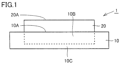
Fig. 1, a silicon carbide substrate 1 in the present embodiment includes a
base substrate
10 composed of silicon carbide and an SiC layer 20 composed of single crystal
silicon
carbide different from base substrate 10 and arranged on base substrate 10 in
contact
therewith.
With such a structure, in silicon carbide substrate 1, base substrate 10
composed
of silicon carbide crystal, for example, high in fault density and low in
quality can be
worked to prescribed shape and size so that silicon carbide single crystal not
having a
desired shape or the like although being of high quality can be arranged on
base
substrate 10 as SiC layer 20. Such silicon carbide substrates 1 are uniform in
prescribed shape and size, and thus more efficient manufacturing of a
semiconductor
device can be achieved. In addition, since semiconductor devices can be
-16-
CA 02761428 2011-11-08 110034:910089
manufactured with the use of SiC layers 20 of high quality for silicon carbide
substrates
1, effective use of silicon carbide single crystal can be made. Consequently,
silicon
carbide substrate 1 in the present embodiment is a silicon carbide substrate
allowing
reduction in cost for manufacturing a semiconductor device.
Here, in silicon carbide substrate 1, base substrate 10 is preferably composed
of
single crystal silicon carbide. Thus, difference in various physical property
values
from SiC layer 20 composed of single crystal silicon carbide becomes small,
and hence
a silicon carbide substrate stable in particular in a process for
manufacturing a
semiconductor device under various environments is obtained.
In silicon carbide substrate 1 above, preferably, SiC layer 20 is lower in
micropipe density than base substrate 10. In addition, in silicon carbide
substrate 1,
preferably, SiC layer 20 is lower in threading screw dislocation density than
base
substrate 10. In addition, in silicon carbide substrate 1, preferably, SiC
layer 20 is
lower in threading edge dislocation density than base substrate 10. In
addition, in
silicon carbide substrate 1, preferably, SiC layer 20 is lower in basal plane
dislocation
density than base substrate 10. In addition, in silicon carbide substrate 1,
preferably,
SiC layer 20 is lower in composite dislocation density than base substrate 10.
In
addition, in silicon carbide substrate 1, preferably, SiC layer 20 is lower in
stacking
fault density than base substrate 10. In addition, in silicon carbide
substrate 1,
preferably, SiC layer 20 is lower in point defect density than base substrate
10.
Silicon carbide substrate I allowing manufacturing of a semiconductor device
of high
quality can be obtained by thus arranging SiC layer 20 lower in fault density
than base
substrate 10. Further, in silicon carbide substrate 1, preferably, SiC layer
20 is smaller
in a full width at half maximum of X-ray rocking curve than SiC layer 20.
Thus,
silicon carbide substrate I allowing manufacturing of a semiconductor device
of high
quality can be obtained by arranging SiC layer 20 smaller in a full width at
half
maximum of X-ray rocking curve, that is, higher in crystallinity, than base
substrate 10.
Referring again to Fig. 1, in silicon carbide substrate 1, base substrate 10
may
-17-
CA 02761428 2011-11-08 110034 : 910089
include a single crystal layer I OB composed of single crystal silicon carbide
so as to
include a main surface IOA on the side facing SiC layer 20. By doing so, in
manufacturing a semiconductor device including silicon carbide substrate 1,
such a
state of a large thickness as readily being handled is maintained in an early
stage of the
manufacturing process, and during the manufacturing process, a region IOC of
the base
substrate other than single crystal layer l OB is removed to allow only single
crystal
layer l OB of base substrate 10 to remain in the inside of the semiconductor
device.
Thus, a semiconductor device of high quality can be manufactured while
handling of
silicon carbide substrate 1 in the manufacturing process is facilitated.
In addition, in silicon carbide substrate 1, SiC layer 20 is preferably lower
in
micropipe density than single crystal layer IOB. In addition, in silicon
carbide
substrate 1, preferably, SiC layer 20 is lower in threading screw dislocation
density than
single crystal layer I OB. In addition, in silicon carbide substrate 1,
preferably, SiC
layer 20 is lower in threading edge dislocation density than single crystal
layer I OB.
In addition, in silicon carbide substrate 1, preferably, SiC layer 20 is lower
in basal
plane dislocation density than single crystal layer l OB above. In addition,
in silicon
carbide substrate I above, preferably, SiC layer 20 is lower in composite
dislocation
density than single crystal layer l OB. In addition, in silicon carbide
substrate 1,
preferably, SiC layer 20 is lower in stacking fault density than single
crystal layer l OB.
In addition, in silicon carbide substrate 1, preferably, SiC layer 20 is lower
in point
defect density than single crystal layer I OB. Thus, silicon carbide substrate
1 allowing
manufacturing of a semiconductor device of high quality can be obtained by
arranging
SiC layer 20 lower in fault density than single crystal layer l OB of base
substrate 10.
In addition, in silicon carbide substrate 1, preferably, SiC layer 20 is
smaller in a
full width at half maximum of X-ray rocking curve than single crystal layer I
OB.
Thus, silicon carbide substrate 1 allowing manufacturing of a semiconductor
device of
high quality can be obtained by arranging SiC layer 20 smaller in a full width
at half
maximum of X-ray rocking curve, that is, higher in crystallinity, than single
crystal
- 18 -
CA 02761428 2011-11-08 110034 : 910089
layer l OB of base substrate 10.
In silicon carbide substrate I in the present embodiment, impurity density in
base substrate 10 can be not lower than 5x10¹⁸ CM-3 . Thus, carrier density in
base
substrate 10 increases and silicon carbide substrate I suitable for
manufacturing a
vertical semiconductor device can be obtained. In addition, impurity
concentration in
base substrate 10 can be higher than 2x 1019 cm 3. Then, impurity
concentration in
SiC layer 20 can be higher than 5x 10¹⁸ CM -3 and lower than 2x 10¹⁹ CM-3 .
Thus,
resistivity in a direction of thickness can be lowered while suppressing
generation of
stacking faults caused by heat treatment.
In silicon carbide substrate 1 in the present embodiment, resistivity of base
substrate 10 can be not lower than lx 105 Q=cm. Thus, a resistance value of
base
substrate 10 increases and silicon carbide substrate I suitable for
manufacturing a
lateral semiconductor device required to adapt to a higher frequency can be
obtained.
In silicon carbide substrate I in the present embodiment, a main surface 20A
of
SiC layer 20 opposite to base substrate 10 may have an off angle with respect
to a plane
orientation {0001 } not smaller than 50 and not greater than 65 . Thus,
silicon
carbide substrate 1 allowing manufacturing of a high-performance semiconductor
device while making effective use of silicon carbide single crystal can be
obtained.
In silicon carbide substrate 1, an angle between an off orientation of main
surface 20A and a <1-100> direction may be not greater than 5 . The <1-100>
direction is a representative off orientation in the silicon carbide
substrate. By setting
variation in off orientation originating from variation or the like in slice
working in the
process for manufacturing silicon carbide substrate 1 to 5 or smaller,
formation or the
like of an epitaxially grown layer on silicon carbide substrate 1 (on main
surface 20A)
can be facilitated. Further, in silicon carbide substrate 1, an off angle of
main surface
20A with respect to a {03-38} plane in the <1-100> direction can be not
smaller than
-3 and not greater than 5 . Thus, channel mobility in a case where a MOSFET
or the
like is fabricated with silicon carbide substrate 1 can further be improved.
-19-
CA 02761428 2011-11-08 110034:910089
Meanwhile, in silicon carbide substrate 1, an angle between an off orientation
of
main surface 20A and a <11-20> direction may be not greater than 5 . Likewise
the
<1-100> direction above, the <1 1-20> direction is a representative off
orientation in a
silicon carbide substrate. By setting variation in off orientation originating
from
variation or the like in slice working in the process for manufacturing
silicon carbide
substrate 1 to 5 , formation or the like of an epitaxially grown layer on SiC
layer 20
can be facilitated.
In silicon carbide substrate 1 in the present embodiment, preferably, main
surface 20A of SiC layer 20 opposite to base substrate 10 is polished. Thus,
an
epitaxially grown layer of high quality can be formed on main surface 20A.
Consequently, a semiconductor device including the epitaxially grown layer of
high
quality, for example, as an active layer, can be manufactured. Namely, by
adopting
such a structure, silicon carbide substrate 1 allowing manufacturing of a high-
quality
semiconductor device including an epitaxial layer formed on SiC layer 20 can
be
obtained.
A method of manufacturing silicon carbide substrate 1 above will now be
described. Referring to Fig. 2, in the method of manufacturing a silicon
carbide
substrate in the present embodiment, initially, a substrate preparation step
is performed
as the step (S 10). In this step (S 10), base substrate 10 composed of silicon
carbide
and SiC substrate 20 composed of single crystal silicon carbide are prepared.
Then, a substrate planarization step is performed as the step (S20). In this
step
(S20), respective main surfaces (bonding surfaces) of base substrate 10 and
SiC
substrate 20 to be in contact with each other in the step (S30) which will be
described
later are planarized, for example, by polishing. Though this step (S20) is not
an
essential step, a size of a gap between base substrate 10 and SiC substrate 20
opposed
to each other becomes uniform by performing this step and hence uniformity in
reaction
(bonding) in the bonding surface in the step (S40) which will be described
later is
improved. Consequently, base substrate 10 and SiC substrate 20 can more
reliably be
-20-
i
CA 02761428 2011-11-08 110034 : 910089
bonded to each other. In addition, in order to further reliably bond base
substrate 10
and the SiC substrate to each other, surface roughness Ra of the bonding
surface above
is preferably less than 100 nm and preferably less than 50 nm. Moreover, by
setting
surface roughness Ra of the bonding surface to less than 10 nm, further
reliable
bonding can be achieved.
On the other hand, the step (S20) may be omitted and the step (S30) may be
performed without polishing respective main surfaces of base substrate 10 and
SiC
substrate 20 to be in contact with each other. Cost for manufacturing silicon
carbide
substrate 1 can thus be reduced. Further, from a point of view of removal of a
damaged layer around the surface caused by slicing or the like at the time of
fabrication
of base substrate 10 and SiC substrate 20, for example, the step of removing
the
damaged layer by etching may be performed instead of or after the step (S20)
above,
and then the step (S30) which will be described later may be performed.
Then, a stacking step is performed as the step (S30). In this step (S30), SiC
substrate 20 is placed on the main surface of base substrate 10 in contact
therewith so
that a stack substrate is fabricated. Here, in this step (S30), main surface
20A of SiC
substrate 20 opposite to base substrate 10 may have an off angle with respect
to the
{0001 } plane not smaller than 50 and not greater than 65 . Thus, silicon
carbide
substrate 1 in which main surface 20A of SiC layer 20 has an off angle with
respect to
the {0001 } plane not smaller than 50 and not greater than 65 can readily be
manufactured. In addition, in step (S30), an angle between an off orientation
of main
surface 20A above and the <1-100> direction maybe not greater than 5 . Thus,
formation or the like of an epitaxially grown layer on fabricated silicon
carbide
substrate 1 (on main surface 20A) can be facilitated. Further, in step (S30),
an off
angle of main surface 20A with respect to a {03-38} plane in the <1-100>
direction
may be not smaller than -3 and not greater than 5 . Thus, channel mobility in
a case
where a MOSFET or the like is fabricated with manufactured silicon carbide
substrate I
can further be improved.
-21-
CA 02761428 2011-11-08 110034 :910089
Meanwhile, in the step (S30), an angle between an off orientation of main
surface 20A and a <11-20> direction may be not greater than 5 . Thus,
formation or
the like of an epitaxially grown layer on fabricated silicon carbide substrate
1 can be
facilitated.
Then, a bonding step is performed as the step (S40). In this step (S40), base
substrate 10 and SiC substrate 20 are bonded to each other by heating the
stack
substrate above. Through the process above, silicon carbide substrate 1 in the
first
embodiment including bonded SiC substrate 20 as SiC layer 20 can readily be
manufactured. In this step (S40), the stack substrate above may be heated in
an
atmosphere obtained by reducing a pressure of an ambient air atmosphere. Thus,
cost
for manufacturing silicon carbide substrate I can be reduced.
Here, in the stack substrate fabricated in the step (S30), a gap formed
between
base substrate 10 and SiC substrate 20 is preferably not greater than 100 m.
Thus,
uniform bonding between base substrate 10 and SiC substrate 20 can be achieved
in the
step (S40).
In the step (S40) above, the stack substrate above is preferably heated to a
temperature range not lower than a sublimation temperature of silicon carbide.
Thus,
base substrate 10 and SiC substrate 20 can more reliably be bonded to each
other. In
particular, by setting a gap formed between base substrate 10 and SiC
substrate 20 to
100 m or smaller in the stack substrate, equal bonding by sublimation of SiC
can be
achieved.
A temperature for heating the stack substrate in the step (S40) is preferably
not
lower than 1800 C and not higher than 2500 C. When a heating temperature is
lower
than 1800 C, it takes long time to achieve bonding between base substrate 10
and SiC
substrate 20 and efficiency in manufacturing silicon carbide substrate I is
lowered.
On the other hand, when a heating temperature exceeds 2500 C, respective
surfaces of
base substrate 10 and SiC substrate 20 roughen and more crystal defects in
fabricated
silicon carbide substrate 1 are likely. In order to improve manufacturing
efficiency
-22-
i
CA 02761428 2011-11-08 110034:910089
while generation of defects in silicon carbide substrate I is further
suppressed, a
temperature for heating the stack substrate in the step (S40) is preferably
not lower than
1900 C and not higher than 2100 C. In addition, by setting a pressure of an
atmosphere during heating in the step (S40) to 10-5 Pa or higher and 106 Pa or
lower,
bonding above can be carried out with a simplified apparatus. Moreover, in
this step
(S40), the stack substrate above may be heated at a pressure higher than 10-1
Pa and
lower than 104 Pa. Thus, bonding above can be carried out with a simplified
apparatus
and an atmosphere for carrying out bonding can be obtained in a relatively
short period
of time, and thus cost for manufacturing silicon carbide substrate I can be
reduced.
Further, an atmosphere during heating in the step (S40) may be an inert gas
atmosphere.
In adopting an inert gas atmosphere as the atmosphere, an inert gas atmosphere
containing at least one selected from the group consisting of argon, helium
and nitrogen
is preferred.
The method of manufacturing silicon carbide substrate 1 in the present
embodiment may further include the step of polishing a main surface of SiC
substrate
corresponding to main surface 20A of SiC substrate 20 opposite to base
substrate 10
in the stack substrate. Thus, silicon carbide substrate 1 in which main
surface 20A of
SiC layer 20 opposite to base substrate 10 is polished can be manufactured.
Here, the
polishing step may be performed before or after bonding between base substrate
10 and
20 SiC substrate 20, so long as it is performed after the step (S 10).
(Second Embodiment)
A second embodiment representing another embodiment of the present
invention will now be described. Referring to Fig. 3, basically, silicon
carbide
substrate 1 in the second embodiment has a construction similar to that of
silicon
carbide substrate 1 in the first embodiment, achieves a similar effect, and
can be
manufactured similarly. Silicon carbide substrate 1 in the second embodiment,
however, is different from that in the first embodiment in that a plurality of
SiC layers
20 are stacked.
-23-
CA 02761428 2011-11-08 110034:910089
Namely, referring to Fig. 3, silicon carbide substrate I in the second
embodiment includes a plurality of (two in the present embodiment) SiC layers
20 on
base substrate 10. Thus, silicon carbide substrate 1 in the present embodiment
is a
silicon carbide substrate including SiC layers 20 in accordance with an
intended
structure of a semiconductor device. More specifically, for example when
silicon
carbide substrate 1 is used for manufacturing a vertical power device
(vertical
MOSFET; Metal Oxide Semiconductor Field Effect Transistor and the like),
impurity
density in base substrate 10 is preferably increased in order to lower
resistivity in a
direction of stack (a direction of thickness) in silicon carbide substrate I
as much as
possible. On the other hand, as impurity density in base substrate 10 is
higher, a
lattice constant of SiC forming base substrate 10 varies. Therefore, when SiC
substrate 20 significantly lower in impurity density than base substrate 10
high in
impurity density is directly bonded onto base substrate 10, strain or warpage
of obtained
silicon carbide substrate I may be great due to difference in lattice constant
between
base substrate 10 and SiC substrate 20 and density of crystal defects may
become high.
In contrast, by sandwiching another SiC substrate 20 of which impurity density
is
intermediate between base substrate 10 high in impurity density and SiC
substrate 20
low in impurity density to thereby gradually vary a lattice constant in a
direction of
thickness of silicon carbide substrate 1, occurrence of such a problem can be
suppressed.
A method of manufacturing silicon carbide substrate 1 according to the second
embodiment will now be described. Silicon carbide substrate 1 according to the
second embodiment can be carried out as in the first embodiment, by stacking a
plurality of (two) SiC substrates 20 on base substrate 10 in the step (S30) in
the method
of manufacturing silicon carbide substrate I in the first embodiment above. On
the
other hand, by adopting the following manufacturing process, silicon carbide
substrate
1 including a plurality of SiC substrates 20 more securely bonded to one
another can be
manufactured.
Namely, referring to Fig. 4, initially, the steps (S 10) to (S40) are
performed as in
-24-
CA 02761428 2011-11-08 110034 : 910089
the first embodiment. Thereafter, in the step (S50), a second stacking step is
performed. In this step (S50), a second stack substrate is fabricated by
further stacking
another SiC substrate 20 on SiC substrate 20 that was stacked on base
substrate 10 in
the step (S30) and bonded to base substrate 10 in the step (S40).
Then, a second bonding step is performed as the step (S60). In this step
(S60),
the stack substrate and another SiC substrate 20 are bonded to each other by
heating the
second stack substrate above as in the step (S40) above. By thus repeatedly
performing the step of placing (stacking) SiC substrate 20 and bonding SiC
substrate 20,
silicon carbide substrate 1 in which a plurality of SiC layers 20 are stacked
can readily
be manufactured.
In the manufacturing method above, respective main surfaces (bonding
surfaces) of SiC substrates 20 to be in contact with each other in the step
(S50) may be
planarized. Here, in order to more reliably bond SiC substrates 20 to each
other,
surface roughness Ra of the bonding surface above is preferably less than 100
nm and
preferably less than 50 nm. Moreover, by setting surface roughness Ra of the
bonding
surface to less than 10 nm, further reliable bonding can be achieved. On the
other
hand, polishing for planarization above may be omitted and the step (S50) may
be
performed without polishing respective main surfaces of SiC substrates 20 to
be in
contact with each other. Cost for manufacturing silicon carbide substrate I
can thus
be reduced. Further, from a point of view of removal of a damaged layer around
the
surface caused by slicing or the like at the time of fabrication of SiC
substrate 20, for
example, the step of removing the damaged layer by etching may be performed
instead
of or after planarization above, and then the step (S50) may be performed.
(Third Embodiment)
A third embodiment representing yet another embodiment of the present
invention will now be described. Referring to Figs. 5 and 6, basically,
silicon carbide
substrate 1 in the third embodiment has a construction similar to that of
silicon carbide
substrate I in the first embodiment, achieves a similar effect, and can be
manufactured
- 25
CA 02761428 2011-11-08 110034 : 910089
similarly. Silicon carbide substrate 1 in the third embodiment, however, is
different
from that in the first embodiment in that a plurality of SiC layers 20 are two-
dimensionally arranged in alignment.
Namely, referring to Figs. 5 and 6, in silicon carbide substrate 1 in the
third
embodiment, a plurality of (nine in the present embodiment) SiC layers 20 are
two-
dimensionally arranged in alignment. Namely, a plurality of SiC layers 20 are
arranged in alignment along main surface IOA of base substrate 10. More
specifically,
nine SiC layers 20 are arranged in matrix such that SiC layers 20 adjacent on
base
substrate 10 are in contact with one another. Thus, silicon carbide substrate
I in the
present embodiment is silicon carbide substrate 1 that can be handled as a
large-
diameter substrate having high-quality SiC layers 20. Then, by employing this
silicon
carbide substrate 1, a process for manufacturing a semiconductor device can be
more
efficient. Referring again to Fig. 5, respective end surfaces 20B of adjacent
SiC layers
are substantially perpendicular to main surface 20A of SiC layer 20. Thus,
silicon
15 carbide substrate 1 in the present embodiment can readily be manufactured.
It is noted
that silicon carbide substrate I in the third embodiment can be manufactured
as in the
first embodiment by two-dimensionally arranging in alignment a plurality of
SiC
substrates 20 of which end surfaces 20B are substantially perpendicular to
main surface
20A in the step (S30).
20 The structures of the silicon carbide substrates in the second and third
embodiments above may be combined with each other. Specifically, for example,
SiC
layer 20 may be arranged on base substrate 10 and a plurality of SiC layers 20
are two-
dimensionally arranged in alignment on SiC layer 20. Such silicon carbide
substrate I
can be manufactured by two-dimensionally placing in alignment a plurality of
SiC
substrates 20 of which end surfaces 20B are substantially perpendicular to
main surface
20A in the step (S50) in the manufacturing method described with reference to
Fig. 4 in
the second embodiment above.
In silicon carbide substrate 1 in the embodiment above, silicon carbide
forming
-26-
i
CA 02761428 2011-11-08 110034 :910089
SiC layer 20 preferably has a hexagonal crystal structure and the crystal
structure is
more preferably 4H-SiC. In addition, base substrate 10 and SiC layer 20 (in a
case
where a plurality of SiC layers 20 are included, adjacent SiC layers 20 as
well) are
preferably composed of silicon carbide single crystal identical in crystal
structure. By
thus adopting silicon carbide single crystal identical in crystal structure
for base
substrate 10 and SiC layer 20, physical properties such as a coefficient of
thermal
expansion are matched up, and warpage of silicon carbide substrate 1,
separation
between base substrate 10 and SiC layer 20, or occurrence of separation
between SiC
layers 20 during the process for manufacturing a silicon carbide substrate and
a
semiconductor device including the silicon carbide substrate can be
suppressed.
Further, in SiC layer 20 and base substrate 10 (in a case where a plurality of
SiC
layers 20 are included, adjacent SiC layers 20 as well), an angle between c
axes of
silicon carbide single crystals forming them is preferably smaller than 1
and more
preferably smaller than 0.1'. Furthermore, preferably, ac plane of silicon
carbide
single crystal does not rotate in the plane.
Base substrate 10 has a diameter preferably not smaller than 2 inches and more
preferably not smaller than 6 inches. In addition, silicon carbide substrate 1
has a
thickness preferably not smaller than 200 m and not greater than 1000 m, and
more
preferably not smaller than 300 m and not greater than 700 m. Further, SiC
layer
20 has resistivity preferably not higher than 50 mQcm and more preferably not
higher
than 20 mQcm.
(Fourth Embodiment)
One example of a semiconductor device fabricated with the silicon carbide
substrate according to the present invention above will now be described as a
fourth
embodiment. Referring to Fig. 7, a semiconductor device 101 according to the
present
invention is a vertical DiMOSFET (Double Implanted MOSFET), and includes a
substrate 102, a buffer layer 121, a breakdown voltage holding layer 122, a p
region 123,
an n+ region 124, a p region 125, an oxide film 126, a source electrode 11 1
and an
-27-
CA 02761428 2011-11-08 110034 : 910089
upper source electrode 127, a gate electrode 110, and a drain electrode 112
formed on a
back surface side of substrate 102. Specifically, buffer layer 121 composed of
silicon
carbide is formed on a surface of substrate 102 composed of silicon carbide
having an n
conductivity type. A silicon carbide substrate according to the present
invention
including silicon carbide substrate I described in the first to third
embodiments above
is adopted as substrate 102. Then, in a case where silicon carbide substrate 1
in the
first to third embodiments above is adopted, buffer layer 121 is formed on SiC
layer 20
of silicon carbide substrate 1. Buffer layer 121 has an n conductivity type
and a
thickness, for example, of 0.5 m. In addition, density of an n-type
conductive
impurity in buffer layer 121 can be, for example, 5x 1017 cm-3. Breakdown
voltage
holding layer 122 is formed on this buffer layer 121. This breakdown voltage
holding
layer 122 is composed of silicon carbide having an n conductivity type and it
has a
thickness, for example, of 10 m. In addition, such a value as 5x10¹⁵ CM -3
can be
adopted as density of an n-type conductive impurity in breakdown voltage
holding layer
122.
In a surface of this breakdown voltage holding layer 122, p regions 123 having
a
p conductivity type are formed at a distance from one another. In the inside
of p
region 123, n+ region 124 is formed in a surface layer of p region 123. In
addition, p+
region 125 is formed at a position adjacent to this n+ region 124. Oxide film
126 is
formed to extend from n+ region 124 in one p region 123 to p region 123,
breakdown
voltage holding layer 122 exposed between two p regions 123, the other p
region 123,
and n+ region 124 in the other p region 123. Gate electrode l 10 is formed on
oxide
film 126. Further, source electrode 111 is formed on n+ region 124 and p+
region 125.
Upper source electrode 127 is formed on this source electrode 111. Moreover,
in
substrate 102, drain electrode 112 is formed on the back surface which is a
surface
opposite to a front surface where buffer layer 121 is formed.
In semiconductor device 101 in the present embodiment, a silicon carbide
substrate according to the present invention such as silicon carbide substrate
1
-28-
CA 02761428 2011-11-08 110034 : 910089
described in the first to third embodiments above is adopted as substrate 102.
Namely,
semiconductor device 101 includes substrate 102 which is a silicon carbide
substrate,
buffer layer 121 and breakdown voltage holding layer 122 as epitaxially grown
and
formed on substrate 102, and source electrode 111 formed on breakdown voltage
holding layer 122. This substrate 102 is a silicon carbide substrate according
to the
present invention such as silicon carbide substrate 1. Here, as described
above, the
silicon carbide substrate according to the present invention is a silicon
carbide substrate
allowing reduction in cost for manufacturing a semiconductor device.
Therefore,
semiconductor device 101 is a semiconductor device of which manufacturing cost
has
been reduced.
A method of manufacturing semiconductor device 101 shown in Fig. 7 will now
be described with reference to Figs. 8 to 12. Referring to Fig. 8, initially,
a substrate
preparation step (S 110) is performed. Here, substrate 102 (see Fig. 9)
composed of
silicon carbide having, for example, a (03-38) plane as the main surface is
prepared.
The silicon carbide substrate according to the present invention above,
including silicon
carbide substrate I manufactured with the manufacturing method described in
the first
to third embodiments above, is prepared as this substrate 102.
Alternatively, a substrate, for example, having an n conductivity type and a
substrate resistance of 0.02 Qcm may be employed as this substrate 102 (see
Fig. 9).
Then, as shown in Fig. 8, an epitaxial layer formation step (S 120) is
performed.
Specifically, buffer layer 121 is formed on the surface of substrate 102. This
buffer
layer 121 is formed on SiC layer 20 (see Figs. 1, 3, and 5) of silicon carbide
substrate I
adopted as substrate 102. An epitaxial layer composed of silicon carbide
having an n
conductivity type and having a thickness, for example, of 0.5 m is formed as
buffer
layer 121. For example, such a value as 5x10'7 cm-3 can be adopted as density
of a
conductive impurity in buffer layer 121. Then, as shown in Fig. 9, breakdown
voltage
holding layer 122 is formed on this buffer layer 121. A layer composed of
silicon
carbide having an n conductivity type is formed as this breakdown voltage
holding layer
-29-
CA 02761428 2011-11-08 110034 : 910089
122 with an epitaxial growth method. For example, such a value as 10 m can be
adopted as a thickness of this breakdown voltage holding layer 122. Further,
such a
value as 5x 1015 cm-3 can be adopted as density of an n-type conductive
impurity in this
breakdown voltage holding layer 122.
Then, as shown in Fig. 8, an implantation step (5130) is performed.
Specifically, using an oxide film formed with photolithography and etching as
a mask,
an impurity having a p conductivity type is implanted into breakdown voltage
holding
layer 122, to thereby form p region 123 as shown in Fig. 10. After the used
oxide film
is removed, an oxide film having a new pattern is again formed with
photolithography
and etching. Then, using this oxide film as a mask, an n-type conductive
impurity is
implanted into a prescribed region to thereby form n+ region 124. By
implanting a
conductive impurity having a p conductivity type with the similar technique,
p+ region
125 is formed. Consequently, a structure as shown in Fig. 10 is obtained.
After such an implantation step, activation annealing treatment is performed.
For example, for this activation annealing treatment, an argon gas is used as
an
atmospheric gas and such conditions as a heating temperature of 1700 C and a
heating
time period of 30 minutes can be employed.
Then, as shown in Fig. 8, a gate insulating film formation step (S 140) is
performed. Specifically, as shown in Fig. 11, oxide film 126 is formed to
cover
breakdown voltage holding layer 122, p region 123, n+ region 124, and p+
region 125.
For example, dry oxidation (thermal oxidation) may be carried out as a
condition for
forming this oxide film 126. Such conditions as a heating temperature of 1200
C and
a heating time period of 30 minutes can be employed as conditions in this dry
oxidation.
Thereafter, as shown in Fig. 8, a nitrogen annealing step (S 150) is
performed.
Specifically, annealing treatment is performed with nitrogen monoxide (NO)
being
employed as an atmospheric gas. As a temperature condition for annealing
treatment,
for example, a heating temperature of 1100 C and a heating time period of 120
minutes
are set. Consequently, nitrogen atoms are introduced in the vicinity of an
interface
-30-
CA 02761428 2011-11-08 110034:910089
between oxide film 126 and each of breakdown voltage holding layer 122, p
region 123,
n+ region 124, and p+ region 125 located below. After this annealing step
using
nitrogen monoxide as the atmospheric gas, annealing using an argon (Ar) gas
which is
an inert gas may further be performed. Specifically, an argon gas is used as
an
atmospheric gas and such conditions as a heating temperature of 1100 C and a
heating
time period of 60 minutes may be adopted.
Then, as shown in Fig. 8, an electrode formation step (S 160) is performed.
Specifically, a resist film having a pattern is formed on oxide film 126 with
photolithography. Using this resist film as a mask, a portion of the oxide
film located
on n+ region 124 and p+ region 125 is etched away. Thereafter, a conductor
film made
of a metal or the like is formed on the resist film and in an opening formed
in oxide
film 126, to be in contact with n+ region 124 and p+ region 125. Thereafter,
by
removing the resist film, the conductor film that has been located on the
resist film is
removed (lift-off). Here, for example, nickel (Ni) can be used as the
conductor.
Consequently, as shown in Fig. 12, source electrode 111 and drain electrode
112 can be
obtained. It is noted that heat treatment for alloying is preferably performed
here.
Specifically, heat treatment (alloying treatment) using, for example, an argon
(Ar) gas
representing an inert gas as an atmospheric gas, with a heating temperature
being set to
950 C and a heating time period being set to 2 minutes, is performed.
Thereafter, upper source electrode 127 (see Fig. 7) is formed on source
electrode 11 1. In addition, gate electrode 110 (see Fig. 7) is formed on
oxide film 126.
Semiconductor device 101 shown in Fig. 7 can thus be obtained.
Though a vertical MOSFET has been described in the fourth embodiment above
by way of example of a semiconductor device that can be fabricated with a
silicon
carbide substrate according to the present invention, a semiconductor device
that can be
fabricated is not limited thereto. For example, various semiconductor devices
such as
a JFET (Junction Field Effect Transistor), an IGBT (Insulated Gate Bipolar
Transistor),
and a Schottky barrier diode can be fabricated with the silicon carbide
substrate
- 31 -
i
CA 02761428 2011-11-08 110034 : 910089
according to the present invention. In addition, though a case of fabricating
a
semiconductor device by forming an epitaxial layer functioning as an operating
layer on
the silicon carbide substrate having a (03-38) plane as the main surface has
been
described in the fourth embodiment above, a crystal plane that can be adopted
as the
main surface above is not limited thereto and any crystal plane in accordance
with
applications including the (0001) plane can be adopted as the main surface
above.
Examples
(Example 1)
Example 1 according to the present invention will be described below.
Various substrates composed of silicon carbide single crystal were prepared
and
experiments for examining whether substrates could be bonded to each other or
not
with a heating temperature being varied were conducted. An experiment
procedure is
as follows.
Initially, an experiment method will be described. Substrates having such
characteristics as shown in Table 1 below were prepared and the substrates
were held
for 3 hours in an inert gas atmosphere at a temperature of 1950 C and at a
pressure of I
Pa in a heating furnace while polished surfaces were in contact with each
other.
Thereafter, a sample was taken out of the heating furnace, whether bonding was
achieved or not was checked, and an angle between c axes of silicon carbide
single
crystals forming adjacent substrates was measured. In a sample A, bonding
between
conductive substrates (substrates 1 and 2) different from each other in
micropipe
density, threading screw dislocation density, threading edge dislocation
density, basal
plane dislocation density, composite dislocation density, and stacking fault
density was
attempted. In addition, in a sample B, bonding between a conductive substrate
(substrate 1) and a semi-insulating substrate (substrate 2) different from
each other in
poly type was attempted. Moreover, in a sample C, bonding among three
substrates
(substrates 1 to 3) was attempted. It is noted that surface roughness Ra in
Table 1
represents roughness at a bonding surface where contact with each other is
made.
-32-
i
CA 02761428 2011-11-08 110034:910089
Here, surface roughness in a square region having one side of 10 m was
measured as
surface roughness Ra. Further, an off angle represents an off angle of a main
surface
with respect to plane orientation (0001) in the <11-20> direction.
Furthermore, "-"
indicates that measurement was not conducted.
In addition, for comparison, an experiment for checking whether bonding could
be achieved or not in samples A to C above by holding them for 3 hours in an
inert gas
atmosphere at a temperature of 1800 C and at a pressure of 133 Pa in a heating
furnace
was also conducted.
/
-33-
CA 02761428 2011-11-08
~^ o
I l o o I I I
a1
00
o 'f ' O O o 0 0
-- o
Q~ x x x x x
rn ~~
O O
OQ' x x l l I I
}; c
n
U Q
N O O
" I
x x
Oa Q Q M ~
C~ O O I I I I
rO~
U O O I I I
Q Q N --~
~~ ~~ I I I I I
x x
00 00
T xxxxxxx M
~ v v v ~r v ~r
o. F..
0 0 0 0 0 0 0
0 0 0 0 0 0 0
0 0 0 0 0 0 0
-9
N ti
t~ ~ -C N N N N N N
.6
Cl`~
N 11]! M
m U
CA 02761428 2011-11-08 110034:910089
Results of the experiment will now be described. In each of samples A to C
for which bonding was carried out under such a condition as holding for 3
hours in an
inert gas atmosphere at a temperature of 1950 C and at a pressure of 1 Pa,
secure
bonding was achieved, An angle between the c axes of silicon carbide single
crystals
forming the substrates in sample A was 0.1 , and an angle between the c axes
in sample
B was 8 . In addition, an angle between the c axes of respective substrates I
and 2 in
sample C was 0.3 , and an angle between the c axes of respective substrates 2
and 3
was 0.1 . Based on this fact, it was confirmed that a silicon carbide
substrate can be
manufactured by bonding substrates different in fault density, conductivity
(impurity
density) and poly type to each other and a silicon carbide substrate can be
manufactured
by bonding three substrates as they are stacked.
On the other hand, bonding could be achieved in none of samples A to C for
which bonding was carried out under such a condition as holding for 3 hours in
an inert
gas atmosphere at a temperature of 1800 C and at a pressure of 133 Pa. Based
on this
fact, it was confirmed that a heating temperature was important in bonding
between
substrates composed of silicon carbide single crystal, and, in order to
efficiently achieve
bonding, a heating temperature was desirably 1950 C or higher, which was equal
to or
higher than a temperature at which SiC sublimated.
Warpage in sample C in which substrates 1, 2 and 3 having n-type impurity
densities of 9x 101 s CM-3 , 3x 10¹⁹ CM -3 and 1 x 10²⁰ CM -3 respectively
were bonded in this
order was 10 um. In contrast, a sample in which substrate I and substrate 3
were
directly bonded to each other was also fabricated, and its warpage was 50 um.
Based
on this fact, it was confirmed that warpage of the bonded substrate could be
lessened by
bonding a substrate high in impurity density and a substrate low in impurity
density
with another substrate having impurity density intermediate therebetween being
interposed so that a lattice constant gradually varied in a direction of
thickness of the
obtained bonded substrate.
(Example 2)
-35-
CA 02761428 2011-11-08 110034:910089
Example 2 according to the present invention will be described below. An
experiment for studying whether substrates of which respective main surfaces
were
greatly inclined with respect to the (0001) plane (substrates each having a
main surface
of which off angle with respect to plane orientation {0001 } was not smaller
than 50
and not greater than 65 ) could be bonded to each other or not and whether a
substrate
of which main surface was greatly inclined with respect to the (0001) plane
and a
substrate having the (0001) plane as the main surface could be bonded to each
other or
not was conducted. An experiment procedure is as follows.
Initially, an experiment method will be described. Substrates having such
characteristics as shown in Table 2 below were prepared and the substrates
were held
for 3 hours in an inert gas atmosphere at a temperature of 1950 C and at a
pressure of I
Pa in a heating furnace while main surfaces were brought in contact with each
other.
Thereafter, the sample was taken out of the heating furnace and whether
bonding was
achieved or not was checked.
Z
- 36 -
i
CA 02761428 2011-11-08
U
O ~
I O O O
N Q U X X X X,
O G
b4= o
UGa..~
GO
C!)
U
o
-o x o
~~+ Q U
O 00 00 ^ 00
y C 00 00 - 00
ccG3 M M O M
y M M G M
A"' O O 0 O
~- x x x x
U In
m M 00 M
c
N M
O O
U G ~i O O
rn ~n
G b G b
o CAN 3 o CN
$ _ $
N N
0) Q) 0) 0)
CO
cn vi V)
LJ.J
cad CO
ai C/) Cl)
i
CA 02761428 2011-11-08 110034 : 910089
Results of the experiment will now be described. In each of samples D and E
for which bonding was carried out under such a condition as holding for 3
hours in an
inert gas atmosphere at a temperature of 1950 C and at a pressure of I Pa,
secure
bonding was achieved. Based on this fact, it was confirmed that the substrate
of
which main surface was greatly inclined with respect to the (0001) plane could
readily
be bonded to both of the substrate of which main surface was similarly greatly
inclined
with respect to the (0001) plane and the substrate having the (0001) plane as
the main
surface.
(Example 3)
An experiment for checking relation of crystal orientation between the base
substrate and the SiC layer in a silicon carbide substrate obtained with the
method of
manufacturing a silicon carbide substrate according to the present invention
was
conducted. An experiment procedure is as follows.
Initially, two substrates (base substrate 10 and SiC substrate 20) each
composed
of SiC and having the (03-38) plane as the main surface were prepared. Then,
the two
substrates were layered such that the main surfaces were in contact with each
other to
fabricate the stack substrate. The stack substrate was heated to 2100 C which
was
equal to or higher than a sublimation temperature of SiC so that the two
substrates were
bonded to each other under such a condition as holding for 30 hours in a
nitrogen gas
atmosphere at a pressure of 1 Pa. A silicon carbide substrate was thus
fabricated.
Here, a temperature of base substrate 10 was maintained at a temperature
slightly higher
than that of SiC substrate 20. Then, crystal orientation in a cross-section
perpendicular to the bonding surface of the obtained silicon carbide substrate
was
examined with an electron back scatter diffraction (EBSD) method.
Results of the experiment will now be described. Referring to Fig. 13, it can
be seen by comparing an EBSD pattern (Fig. 14) at a position A in SiC layer 20
and an
EBSD pattern (Fig. 15) at a position B in base substrate 10, that are arranged
across a
boundary 30, with each other, that these positions match with each other.
Therefore, it
- 38 -
CA 02761428 2011-11-08 110034:910089
can be seen that SiC crystal forming base substrate 10 and SiC crystal forming
SiC
layer 20 are identical in a direction of the c axis and there is no rotation
in the c plane.
This may be because SiC crystal forming base substrate 10 and SiC crystal
forming SiC
layer 20 were identical in crystal orientation as a result of the fact that
bonding between
base substrate 10 and SiC substrate 20 was achieved by sublimation of base
substrate
held at a temperature slightly higher than SiC substrate 20.
(Example 4)
An experiment for examining relation between a size of a gap formed between
the base substrate and the SiC substrate during bonding of the stack substrate
and a
10 state of bonding of the stack substrate was conducted. Initially, as in the
case of
Example 3 above, the two substrates (base substrate 10 and SiC substrate 20)
were
prepared and two substrates were layered such that main surfaces thereof were
brought
in contact with each other. The stack substrate was thus fabricated. Here,
adjustment was made such that a gap formed between the two substrates was from
0.5
to 1000 m wide. Then, as in Example 3 above, the stack substrate above was
heated
to 2100 C and held for 30 hours in a nitrogen gas atmosphere at a pressure of
1 Pa.
Then, a state of bonding of the stack substrate after the treatment was
checked. Table
3 shows results of the experiment.
Table 3
Gap ( m) 0.5 1 10 50 100 200 1000
State of A A A A A B C
Bonding
A: uniform bonding
B: partial bonding
C: bonding unsuccessful
In Table 3, a sample in which two substrates were uniformly bonded to each
other over the entire region was denoted as A, a sample in which only partial
bonding
was achieved was denoted as B, and a sample in which bonding between the two
substrates was unsuccessful was denoted as C. As shown in Table 3, it was
confirmed
-39-
i
CA 02761428 2011-11-08 110034 : 910089
that, in order to achieve uniform bonding, a gap formed between the base
substrate and
the SiC substrate was preferably not greater than 100 m.
As described in the fourth embodiment above, a semiconductor device can be
fabricated with the silicon carbide substrate according to the present
invention.
Namely, in the semiconductor device according to the present invention, an
epitaxially
grown layer serving as an operating layer is formed on the silicon carbide
substrate
manufactured with the method of manufacturing a silicon carbide substrate
according to
the present invention above. Giving the description from a different point of
view, in
the semiconductor device according to the present invention, an epitaxially
grown layer
serving as an operating layer is formed on the silicon carbide substrate
according to the
present invention above. More specifically, the semiconductor device according
to the
present invention includes the silicon carbide substrate according to the
present
invention above, an epitaxially grown layer formed on the silicon carbide
substrate, and
an electrode formed on the epitaxially grown layer. Namely, the semiconductor
device according to the present invention includes a base substrate composed
of silicon
carbide, an SiC layer composed of single crystal silicon carbide and arranged
on the
base substrate in contact therewith, an epitaxially grown layer formed on the
SiC layer,
and an electrode formed on the epitaxially grown layer.
It should be understood that the embodiments and the examples disclosed herein
are illustrative and non-restrictive in every respect. The scope of the
present invention
is defined by the terms of the claims, rather than the description above, and
is intended
to include any modifications within the scope and meaning equivalent to the
terms of
the claims.
INDUSTRIAL APPLICABILITY
A silicon carbide substrate and a method of manufacturing the same according
to the present invention are particularly advantageously applicable to a
silicon carbide
substrate used for manufacturing a semiconductor device required to be low in
manufacturing cost and a method of manufacturing the same. In addition, a
-40-
CA 02761428 2011-11-08 110034 : 910089
semiconductor device according to the present invention is particularly
advantageously
applicable to a semiconductor device required to be low in manufacturing cost.
REFERENCE SIGNS LIST
I silicon carbide substrate; 10 base substrate; I OA main surface; 20 SiC
layer
(SiC substrate); 20A main surface; 20B end surface; 30 boundary; 101
semiconductor
device; 102 substrate; 110 gate electrode; 111 source electrode; 112 drain
electrode;
121 buffer layer; 122 breakdown voltage holding layer; 123 p region; 124 n+
region;
125 p+ region; 126 oxide film; and 127 upper source electrode.
-41-