Note: Descriptions are shown in the official language in which they were submitted.
CA 02761430 2011-11-08 110061:910136
DESCRIPTION
TITLE OF INVENTION
Silicon Carbide Substrate and Semiconductor Device
TECHNICAL FIELD
The present invention relates to a silicon carbide substrate and a
semiconductor
device, more particularly, a silicon carbide substrate allowing for reduced
resistivity in
the thickness direction thereof while restraining stacking faults from being
produced
due to heat treatment, as well as a semiconductor device including such a
silicon
carbide substrate.
BACKGROUND ART
In recent years, in order to achieve high breakdown voltage, low loss, and
utilization of semiconductor devices under a high temperature environment,
silicon
carbide (SiC) has begun to be adopted as a material for a semiconductor
device.
Silicon carbide is a wide band gap semiconductor having a band gap larger than
that of
silicon, which has been conventionally widely used as a material for
semiconductor
devices. Hence, by adopting silicon carbide as a material for a semiconductor
device,
the semiconductor device can have a high breakdown voltage, reduced on-
resistance,
and the like. Further, the semiconductor device thus adopting silicon carbide
as its
material has characteristics less deteriorated even under a high temperature
environment than those of a semiconductor device adopting silicon as its
material,
advantageously.
In order to manufacture the high-performance semiconductor device adopting
silicon carbide as its material, it is effective to employ a process of
preparing a substrate
made of silicon carbide (silicon carbide substrate), and forming an epitaxial
growth
layer made of SiC on the silicon carbide substrate. Further, on-resistance of
the device
can be reduced by reducing resistivity of the substrate in the thickness
direction thereof
as much as possible when manufacturing, for example, a vertical type power
device
-I-
CA 02761430 2011-11-08 110061:910136
(such as a vertical type MOSFET (Metal Oxide Semiconductor Field Effect
Transistor)
using the silicon carbide substrate. Further, in order to reduce the
resistivity of the
substrate in the thickness direction thereof, for example, there can be
employed a
method of introducing an impurity, which is an n type dopant such as nitrogen,
into the
substrate at a high concentration (for example, see R. C. GLASS et al., "SiC
Seeded
Crystal Growth", Phys. stat. sol. (b), 1997, 202, p149-162 (Non-Patent
Literature 1)).
CITATION LIST
NON PATENT LITERATURE
NPL 1: R. C. GLASS et al., "SiC Seeded Crystal Growth", Phys. stat. sol.(b),
1997, 202, p 149-162
SUMMARY OF INVENTION
TECHNICAL PROBLEM
However, if the resistivity of the substrate is reduced by simply introducing
the
impurity into the substrate at a high concentration, the following problem
takes place.
That is, when fabricating a semiconductor device using the silicon carbide
substrate, the
silicon carbide substrate is subjected to heat treatment such as thermal
cleaning for
cleaning a surface of the silicon carbide substrate. On this occasion,
stacking faults
are produced in the silicon carbide substrate containing the impurity at a
high
concentration. When an epitaxial growth layer made of SiC is formed on the
silicon
carbide substrate, the stacking faults are propagated to the SiC layer. Here,
assuming
that the SiC constituting the silicon carbide substrate is for example 4H-SiC,
each of
the stacking faults to be produced has a structure of 3C type, which has a
band gap
smaller than that in the 4H type. Accordingly, the band gap becomes smaller
locally
in the region in which the stacking faults are produced. As a result, if a
semiconductor
device is fabricated using such a silicon carbide substrate, problems will
take place such
as reduced breakdown voltage and increased leakage current.
In view of this, the present invention has its object to provide a silicon
carbide
substrate allowing for reduced resistivity in the thickness direction thereof
while
-2-
CA 02761430 2011-11-08 110061:910136
restraining stacking faults from being produced due to heat treatment, as well
as a
semiconductor device including such a silicon carbide substrate.
SOLUTION TO PROBLEM
A silicon carbide substrate according to the present invention includes: a
base
layer made of silicon carbide; and a SiC layer made of single-crystal silicon
carbide and
disposed on the base layer. The base layer has an impurity concentration
greater than
2 x 10¹⁹ CM-3 . The SiC layer has an impurity concentration greater than 5 x
101 8 cm-3
and smaller than 2 x 1019 cm 3. The SiC layer and the base layer are in
contact with
each other. The SiC layer and the base layer are connected to each other.
The present inventors have fully studied approaches for reducing resistivity
of a
silicon carbide substrate in the thickness direction thereof while restraining
stacking
faults from being produced due to heat treatment. As a result, it has been
found that
when the impurity concentration thereof is less than 2 x 1019 cm 3, stacking
faults can
be prevented from being produced due to heat treatment, but are unlikely to be
prevented when the impurity concentration exceeds 2 x 10¹⁹ em-3. Thus,
stacking
faults can be prevented from being produced at least in the SiC layer even
when heat
treatment is performed in a subsequent device process, by providing the
silicon carbide
substrate with the layer (base layer) having an impurity concentration greater
than 2 x
1019 CM -3 and a small resistivity and the layer (SiC layer) disposed on the
base layer and
having an impurity concentration smaller than 2 x 1019 cm-3. Further, by
forming an
epitaxial growth layer made of silicon carbide on such a SiC layer so as to
fabricate the
semiconductor device, the resistivity of the silicon carbide substrate can be
reduced by
the existence of the base layer, while preventing influence of stacking
faults, which can
be produced in the base layer, over the characteristics of the semiconductor
device.
Meanwhile, when the SiC layer has an impurity concentration of 5 x 1018 cm-3
or
smaller, the resistivity of the SiC layer becomes too large,
disadvantageously.
In this way, according to the silicon carbide substrate of the present
invention, there can be provided a silicon carbide substrate allowing for
reduced resistivity in the thickness direction thereof while restraining
stacking faults from being produced due to
-3 E
CA 02761430 2011-11-08 110061:910136
heat treatment. Here, the term "impurity" refers to an impurity to be
introduced to
produce a majority carrier in the silicon carbide substrate.
The silicon carbide substrate may further include an epitaxial growth layer
formed on the SiC layer and made of single-crystal silicon carbide, wherein
the
epitaxial growth layer has a stacking fault density smaller than that in the
base layer.
In forming an epitaxial growth layer on the SIC layer, for example, it is
necessary to thermally clean the silicon carbide substrate or heat the
substrate during
the epitaxial growth. Even if the heating causes production of stacking faults
in the
base layer, the stacking faults can be restrained from being produced at least
in the SiC
layer as described above. Hence, also in the epitaxial growth layer formed on
the SiC
layer, stacking faults can be restrained from being produced. As a result,
this silicon
carbide substrate has the epitaxial growth layer with stacking faults being
restrained
from being produced therein while allowing for reduced resistivity. Hence, the
silicon
carbide substrate can be used to fabricate a semiconductor device that
suppresses
reduced breakdown voltage and increased leakage current. It should be noted
that this
epitaxial growth layer can be used as, for example, a buffer layer or a
breakdown
voltage holding layer (drift layer) in the semiconductor device.
In the silicon carbide substrate, the impurity contained in the base layer may
be
different from that contained in the SiC layer. In this way, a silicon carbide
substrate
can be provided which contains impurities appropriately depending on intended
purpose of use.
In the silicon carbide substrate, the impurity contained in the base layer can
be
nitrogen or phosphorus, and the impurity contained in the SiC layer can be
nitrogen or
phosphorus. Each of nitrogen and phosphorus is suitable as an impurity for
supplying
the SiC with electrons, which serve as majority carriers.
In the silicon carbide substrate, a plurality of the SiC layers may be
arranged
side by side when viewed in a planar view. Explaining from a different point
of view,
the plurality of SiC layers may be arranged on and along the main surface of
the base
-4-
CA 02761430 2011-11-08 110061:910136
layer.
SiC does not have a liquid phase at an atmospheric pressure. In addition,
crystal growth temperature thereof is 2000 C or greater, which is very high.
This
makes it difficult to control and stabilize growth conditions. Hence, it is
difficult for a
substrate made of single-crystal SiC to keep its high quality and have a large
diameter.
To address this, the plurality of SiC layers each obtained from a high-quality
silicon
carbide single-crystal are arranged side by side on the base layer having a
large
diameter when viewed in a planar view, thereby obtaining a silicon carbide
substrate
that can be handled as a substrate having a high-quality SiC layer and a large
diameter.
By using such a silicon carbide substrate, the process of manufacturing a
semiconductor
device can be improved in efficiency. It should be noted that in order to
improve the
efficiency of the process of manufacturing a semiconductor device, it is
preferable that
adjacent ones of the plurality of SiC layers are arranged in contact with one
another.
More specifically, for example, the plurality of SiC layers are preferably
arranged in
contact with one another in the form of a matrix. Further, each of adjacent
SiC layers
preferably has an end surface substantially perpendicular to the main surface
thereof.
In this way, the silicon carbide substrate can be readily formed. Here, for
example,
when the end surface and the main surface form an angle of not less than 85
and not
more than 95 , it can be determined that the end surface and the main surface
are
substantially perpendicular to each other.
In the silicon carbide substrate, the base layer may be made of single-crystal
silicon carbide, and a half width of X-ray rocking curve of the SiC layer may
be smaller
than that of the base layer.
As described above, it is difficult for a high-quality single-crystal silicon
carbide
to have a large diameter. Meanwhile, for efficient manufacturing in a process
of
manufacturing a semiconductor device using a silicon carbide substrate, a
substrate
provided with predetermined uniform shape and size is required. Hence, even
when a
high-quality silicon carbide single-crystal (for example, single-crystal
silicon carbide
-5-
CA 02761430 2011-11-08
110061:910136
having a high crystallinity) is obtained, a region that cannot be processed
into such a
predetermined shape and the like by cutting, etc., may not be effectively
used.
To address this, in the silicon carbide substrate of the present invention, on
the
base layer processed into the predetermined shape and size, there can be
disposed the
SiC layer having a smaller half width of the X-ray rocking curve, i.e., having
higher
crystallinity than that of the base layer but not formed into the desired
shape and the
like. Such a silicon carbide substrate has the predetermined uniform shape and
size,
thus attaining effective manufacturing of semiconductor devices. Further, such
a
silicon carbide substrate utilizes the high-quality SiC layer to manufacture a
semiconductor device, thereby effectively utilizing the high-quality single-
crystal
silicon carbide. As a result, the manufacturing cost of the semiconductor
device using
the silicon carbide substrate can be reduced.
In the silicon carbide substrate, the base layer may be made of single-crystal
silicon carbide, and the SiC layer may have a micro pipe density lower than
that of the
base layer.
Further, in the silicon carbide substrate, the base layer may be made of
single-
crystal silicon carbide, and the SiC layer may have a dislocation density
lower than that
of the base layer.
Further, in the silicon carbide substrate, the base layer is made of single-
crystal
silicon carbide, and the SiC layer may have a threading screw dislocation
density
smaller than that of the base layer.
Further, in the silicon carbide substrate, the base layer is made of single-
crystal
silicon carbide, and the SiC layer may have a threading edge dislocation
density smaller
than that of the base layer.
Further, in the silicon carbide substrate, the base layer is made of single-
crystal
silicon carbide, and the SiC layer may have a basal plane dislocation density
smaller
than that of the base layer.
Further, in the silicon carbide substrate, the base layer is made of single-
crystal
-6-
CA 02761430 2011-11-08
110061:910136
silicon carbide, and the SiC layer may have a mixed dislocation density
smaller than
that of the base layer.
Further, in the silicon carbide substrate, the base layer is made of single-
crystal
silicon carbide, and the SiC layer may have a stacking fault density smaller
than that of
the base layer.
Further, in the silicon carbide substrate, the base layer is made of single-
crystal
silicon carbide, and the SiC layer may have a point defect density smaller
than that of
the base layer.
Accordingly, on the relatively low-quality but low-cost base layer processed
into
the predetermined shape and size suitable for manufacturing of a semiconductor
device,
there can be disposed the high-quality SiC layer not having the predetermined
shape
and size and having smaller micro pipe density and dislocation densities than
those of
the base layer (such as the threading screw dislocation density, the threading
edge
dislocation density, the basal plane dislocation density, the mixed
dislocation density,
the stacking fault density, and the point defect density). Such a silicon
carbide
substrate has the predetermined uniform shape and size suitable for
manufacturing of a
semiconductor device as a whole, thus attaining effective manufacturing of
semiconductor devices. Further, such a silicon carbide substrate utilizes the
high-
quality SiC layer to manufacture a semiconductor device, thereby effectively
utilizing
the high-quality single-crystal silicon carbide. As a result, the
manufacturing cost of
the semiconductor device using the silicon carbide substrate can be reduced.
In the silicon carbide substrate, the base layer may include a single-crystal
layer
made of single-crystal silicon carbide and including its main surface facing
the SiC
layer. With this, in an early stage of a process of manufacturing a
semiconductor
device using the silicon carbide substrate, the silicon carbide substrate is
maintained to
have its large thickness and is therefore readily handled, and in the middle
of the
process of manufacturing, a region of the base layer other than the single-
crystal layer is
removed, whereby only the single-crystal layer of the base layer can remain
within the
-7-
{
CA 02761430 2011-11-08
110061: 910136
semiconductor device. In this way, a high-quality semiconductor device can be
manufactured while facilitating handling of the silicon carbide substrate in
the process
of manufacturing.
In the silicon carbide substrate, a half width of X-ray rocking curve of the
SiC
layer may be smaller than that of the single-crystal layer. As such, the SiC
layer
having such a smaller half width of the X-ray rocking curve, i.e., higher
crystallinity
than that of the single-crystal layer of the base layer is provided, thereby
obtaining a
silicon carbide substrate by which a high-quality semiconductor device can be
obtained.
In the silicon carbide substrate, the SiC layer may have a micro pipe density
lower than that of the single-crystal layer.
Further, in the silicon carbide substrate, the SiC layer may have a
dislocation
density lower than that of the single-crystal layer.
Further, in the silicon carbide substrate, the SiC layer may have a threading
screw dislocation density smaller than that of the single-crystal layer.
Further, in the silicon carbide substrate, the SiC layer may have a threading
edge
dislocation density smaller than that of the single-crystal layer.
Further, in the silicon carbide substrate, the SiC layer may have a basal
plane
dislocation density smaller than that of the single-crystal layer.
Further, in the silicon carbide substrate, the SiC layer may have a mixed
dislocation density smaller than that of the single-crystal layer.
Further, in the silicon carbide substrate, the SiC layer may have a stacking
fault
density smaller than that of the single-crystal layer.
Further, in the silicon carbide substrate, the SiC layer may have a point
defect
density smaller than that of the single-crystal layer.
Thus, as compared with the single-crystal layer of the base layer, the SiC
layer
has the reduced defect densities such as the micro pipe density, the threading
screw
dislocation density, the threading edge dislocation density, the basal plane
dislocation
density, the mixed dislocation density, stacking fault density, and the point
defect
-8-
CA 02761430 2011-11-08 110061:910136
density. With the SiC layer, the silicon carbide substrate allowing for
manufacturing a
high-quality semiconductor device can be obtained.
In the silicon carbide substrate, the SiC layer may have a main surface
opposite
to the base layer and having an off angle of not less than 50 and not more
than 65
relative to a {0001 } plane.
By growing single-crystal silicon carbide of hexagonal system in the <0001>
direction, a high-quality single-crystal can be fabricated efficiently. From
such a
silicon carbide single-crystal grown in the <0001> direction, a silicon
carbide substrate
having a main surface corresponding to the {0001) plane can be obtained
efficiently.
Meanwhile, by using a silicon carbide substrate having a main surface having
an off
angle of not less than 50 and not more than 65 relative to the plane
orientation of
{0001 }, a semiconductor device with high performance may be manufactured.
Specifically, for example, a silicon carbide substrate used for fabrication of
a
MOSFET generally has a main surface having an off angle of approximately 8
relative
to a plane orientation of {0001 }. An epitaxial growth layer is formed on this
main
surface and an oxide film, an electrode, and the like are formed on this
epitaxial growth
layer, thereby obtaining a MOSFET. In this MOSFET, a channel region is formed
in a
region including an interface between the epitaxial growth layer and the oxide
film.
However, in the MOSFET having such a structure, a multiplicity of interface
states are
formed around the interface between the epitaxial growth layer and the oxide
film, i.e.,
the location in which the channel region is formed, due to the substrate's
main surface
having an off angle of approximately 8 or smaller relative to the plane
orientation of
10001). This hinders traveling of carriers, thus decreasing channel mobility.
To address this, in the silicon carbide substrate, the main surface of the SiC
layer opposite to the base layer is adapted to have an off angle of not less
than 50 and
not more than 65 relative to the {0001 } plane, thereby reducing formation of
the
interface states. In this way, a MOSFET can be fabricated which allows for
reduced
on-resistance.
-9-
CA 02761430 2011-11-08 110061:910136
In the silicon carbide substrate, the main surface of the SiC layer opposite
to the
base layer may have an off orientation forming an angle of 5 or smaller
relative to a
<1-100> direction.
The <1-100> direction is a representative off orientation in a silicon carbide
substrate. Variation in the off orientation resulting from variation in a
slicing process
of the process of manufacturing the substrate is adapted to be 5 or smaller,
which
allows an epitaxial growth layer to be formed readily on the silicon carbide
substrate.
In the silicon carbide substrate, the main surface of the SiClayer opposite to
the
base layer may have an off angle of not less than -3 and not more than 5
relative to a
{03-38} plane in the <1-100> direction. Accordingly, channel mobility can be
further
improved in the case where a MOSFET is fabricated using the silicon carbide
substrate.
Here, setting the off angle at not less than -3 and not more than +5
relative to the
plane orientation of {03-38} is based on a fact that particularly high channel
mobility
was obtained in this set range as a result of inspecting a relation between
the channel
mobility and the off angle.
Further, the "off angle relative to the {03-38} plane in the <1-100>
direction"
refers to an angle formed by an orthogonal projection of a normal line of the
above-
described main surface to a flat plane defined by the <1-100> direction and
the <0001>
direction, and a normal line of the {03-38} plane. The sign of positive value
corresponds to a case where the orthogonal projection approaches in parallel
with the
<1-100> direction whereas the sign of negative value corresponds to a case
where the
orthogonal projection approaches in parallel with the <0001> direction.
It should be noted that the main surface preferably has a plane orientation of
substantially {03-38}, and the main surface more preferably has a plane
orientation of
{03-38}. Here, the expression "the main surface has a plane orientation of
substantially {03-38}" is intended to encompass a case where the plane
orientation of
the main surface of the substrate is included in a range of off angle such
that the plane
orientation can be substantially regarded as {03-38} in consideration of
processing
-10-
CA 02761430 2011-11-08 110061:910136
accuracy of the substrate. In this case, the range of off angle is, for
example, a range
of off angle of 2 relative to {03-38}. Accordingly, the above-described
channel
mobility can be further improved.
In the silicon carbide substrate, the main surface opposite to the base layer
may
have an off orientation forming an angle of 5 or smaller relative to a <11-
20> direction.
<11-20> is a representative off orientation in a silicon carbide substrate, as
with
the <1-100> direction. Variation in the off orientation resulting from
variation in the
slicing process of the process of manufacturing the substrate is adapted to
be* 5 ,
which allows an epitaxial growth layer to be formed readily on the SiC layer.
A semiconductor device according to the present invention includes: a silicon
carbide substrate; an epitaxial growth layer formed on the silicon carbide
substrate; and
an electrode formed on the epitaxial growth layer. The silicon carbide
substrate is the
above-described silicon carbide substrate of the present invention.
Because the semiconductor device of the present invention includes the above-
described silicon carbide substrate of the present invention, there can be
provided a
semiconductor device allowing for reduced resistivity in the thickness
direction of the
substrate while restraining stacking faults from being produced.
ADVANTAGEOUS EFFECTS OF INVENTION
As apparent from the description above, according to the silicon carbide
substrate of the present invention, there can be provided a silicon carbide
substrate
allowing for reduced resistivity in the thickness direction thereof while
restraining
stacking faults from being produced due to heat treatment. Further, according
to the
semiconductor device of the present invention, there can be provided a
semiconductor
device allowing for reduced resistivity in the thickness direction of the
substrate while
restraining stacking faults from being produced.
BRIEF DESCRIPTION OF DRAWINGS
Fig. I is a schematic cross sectional view showing a structure of a silicon
carbide substrate.
-Il-
CA 02761430 2011-11-08
110061: 910136
Fig. 2 is a schematic cross sectional view showing the structure of the
silicon
carbide substrate having an epitaxial layer formed thereon.
Fig. 3 is a flowchart schematically showing a method for manufacturing the
silicon carbide substrate.
Fig. 4 is a flowchart schematically showing another method for manufacturing
the silicon carbide substrate.
Fig. 5 is a schematic cross sectional view for illustrating the method for
manufacturing the silicon carbide substrate.
Fig. 6 is a schematic cross sectional view for illustrating the method for
manufacturing the silicon carbide substrate.
Fig. 7 is a schematic cross sectional view for illustrating the method for
manufacturing the silicon carbide substrate.
Fig. 8 is a schematic cross sectional view showing another structure of the
silicon carbide substrate.
Fig. 9 is a schematic cross sectional view showing still another structure of
the
silicon carbide substrate.
Fig. 10 is a flowchart schematically showing a method for manufacturing the
silicon carbide substrate of Fig. 9.
Fig. 11 is a schematic cross sectional view showing yet another structure of
the
silicon carbide substrate.
Fig. 12 is a flowchart schematically showing a method for manufacturing the
silicon carbide substrate of Fig. 11.
Fig. 13 is a schematic cross sectional view showing a structure of a vertical
type
MOSFET.
Fig. 14 is a flowchart schematically showing a method for manufacturing the
vertical type MOSFET.
Fig. 15 is a schematic cross sectional view for illustrating the method for
manufacturing the vertical type MOSFET.
-12-
CA 02761430 2011-11-08
11006]:9]0136
Fig. 16 is a schematic cross sectional view for illustrating the method for
manufacturing the vertical type MOSFET.
Fig. 17 is a schematic cross sectional view for illustrating the method for
manufacturing the vertical type MOSFET.
Fig. 18 is a schematic cross sectional view for illustrating the method for
manufacturing the vertical type MOSFET.
DESCRIPTION OF EMBODIMENTS
The following describes embodiments of the present invention with reference to
figures. It should be noted that in the below-mentioned figures, the same or
corresponding portions are given the same reference characters and are not
described
repeatedly.
(First Embodiment)
First, one embodiment of the present invention, i.e., a first embodiment will
be
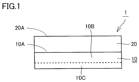
described. Referring to Fig. 1. a silicon carbide substrate I of the present
embodiment
includes: a base layer 10 made of silicon carbide; and a SiC layer 20 made of
single-
crystal silicon carbide and disposed on one main surface I OA of base layer
10. Base
layer 10 has an impurity concentration greater than 2 x 1019 cm-3. SiC layer
20 has an
impurity concentration greater than 5 x 1018 cm-3 and smaller than 2 x 1019 cm-
3.
Even when silicon carbide substrate I is provided with base layer 10 thus
having an impurity concentration greater than 2 x 1019 cm"3 and having a small
resistivity, SiC layer 20 having an impurity concentration smaller than 2 x
1019 cm-3
and provided on base layer 10 restrains stacking faults from being produced at
least in
SiC layer 20 if heat treatment is performed in a subsequent device process.
Then, when an epitaxial growth layer 30 made of single-crystal silicon carbide
is formed on main surface 20A of SiC layer 20 opposite to base layer 10 as
shown in
Fig. 2, stacking faults that can be generated in base layer 10 are not
propagated to
epitaxial growth layer 30. Accordingly, stacking fault density in epitaxial
growth layer
is smaller than that in base layer 10.
-13-
CA 02761430 2011-11-08
110061:910136
Thus, silicon carbide substrate 1 allows for reduced resistivity in the
thickness
direction thereof while restraining stacking faults from being produced due to
heat
treatment in a device manufacturing process.
Here, in silicon carbide substrate 1, the impurity contained in base laver 10
may
be different from that contained in SiC layer 20. In this way, there can be
obtained a
silicon carbide substrate containing impurities appropriately depending on
intended
purpose of use. Further, the impurity contained in base layer 10 may be
nitrogen or
phosphorus, whereas the impurity contained in SiC layer 20 may be also
nitrogen or
phosphorus.
Further, in silicon carbide substrate 1, base layer 10 is made of single-
crystal
silicon carbide, and the half width of X-ray rocking curve of SiC layer 20 may
be
smaller than that of base layer 10.
Accordingly, a single-crystal silicon carbide having predetermined uniform
shape and size and having relatively low crystallinity is employed as base
laver 10 of
silicon carbide substrate 1, while a single-crystal silicon carbide having a
high
crystallinity and not having the desired shape or the like is effectively
utilized as SiC
layer 20. As a result, by fabricating a semiconductor device using such a
silicon
carbide substrate 1, manufacturing cost of the semiconductor device can be
reduced.
Further, in silicon carbide substrate 1, base layer 10 may be made of single-
crystal silicon carbide, and SiC layer 20 may have a micro pipe density lower
than that
of base layer 10. Further, in silicon carbide substrate 1, base layer 10 may
be made of
single-crystal silicon carbide, and SiC layer 20 may have a dislocation
density lower
than that of base layer 10. Further, in silicon carbide substrate 1, base
layer 10 may be
made of single-crystal silicon carbide, and SiC layer 20 may have a threading
screw
dislocation density smaller than that of base layer 10. Further, in silicon
carbide
substrate 1, base layer 10 may be made of single-crystal silicon carbide, and
SiC layer
20 may have a threading edge dislocation density smaller than that of base
layer 10.
Further, in silicon carbide substrate 1, base layer 10 may be made of single-
crystal
-14-
CA 02761430 2011-11-08
110061:910136
silicon carbide, and SiC layer 20 may have a basal plane dislocation density
smaller
than that of base layer 10. Further, in silicon carbide substrate 1, base
layer 10 may be
made of single-crystal silicon carbide, and SiC layer 20 may have a mixed
dislocation
density smaller than that of base layer 10. Further, in silicon carbide
substrate 1, base
layer 10 may be made of single-crystal silicon carbide, and SiC layer 20 may
have a
stacking fault density smaller than that of base layer 10. Further, in silicon
carbide
substrate 1, base layer 10 may be made of single-crystal silicon carbide, and
SiC layer
20 may have a point defect density smaller than that of base layer 10.
Accordingly, a single-crystal silicon carbide having predetermined uniform
shape and size and having a relatively low quality is employed as base layer
10 of
silicon carbide substrate 1, while a single-crystal silicon carbide having a
high quality
and not having the desired shape or the like is effectively utilized as SiC
layer 20.
Thus, by fabricating a semiconductor device using such a silicon carbide
substrate 1,
manufacturing cost of the semiconductor device can be reduced.
Further, in silicon carbide substrate 1, base layer 10 may include a single-
crystal
layer I OB made of single-crystal silicon carbide and including main surface I
OA
located at a side facing SiC layer 20. With this, in an early stage of a
process of
manufacturing a semiconductor device using silicon carbide substrate 1.
silicon carbide
substrate I is maintained to have its large thickness and is therefore readily
handled,
and in the middle of the process of manufacturing, a region I OC of base layer
10 other
than the single-crystal layer is removed, whereby only single-crystal layer 1
OB of base
layer 10 can remain within the semiconductor device. In this way, a high-
quality
semiconductor device can be manufactured while facilitating handling of
silicon
carbide substrate I in the process of manufacturing.
Further, in silicon carbide substrate 1, the half width of X-ray rocking curve
of
SiC layer 20 may be smaller than that of single-crystal layer 10B. As such,
SiC layer
20 having such a smaller half width of the X-ray rocking curve, i.e., having
higher
crystallinity than that of single-crystal layer l OB of base layer 10 is
provided, thereby
-15-
CA 02761430 2011-11-08
110061:910136
obtaining silicon carbide substrate I by which a high-quality semiconductor
device can
be manufactured. Further, in silicon carbide substrate 1, SiC layer 20 may
have a
micro pipe density lower than that of single-crystal layer IOB. Further. in
silicon
carbide substrate 1, SiC layer 20 may have a dislocation density lower than
that of
single-crystal layer I OB. Further, in silicon carbide substrate 1, SiC layer
20 may have
a threading screw dislocation density smaller than that of single-crystal
layer I OB.
Further, in silicon carbide substrate 1, SiC layer 20 may have a threading
edge
dislocation density smaller than that of single-crystal layer 10B. Further, in
silicon
carbide substrate 1, SiC layer 20 may have a basal plane dislocation density
smaller
than that of single-crystal layer I OB. Further, in silicon carbide substrate
1, SiC layer
may have a mixed dislocation density smaller than that of single-crystal layer
I OB.
Further, in silicon carbide substrate 1, SiC layer 20 may have a stacking
fault density
smaller than that of single-crystal layer I OB. Further, in silicon carbide
substrate 1,
SiC layer 20 may have a point defect density smaller than that of single-
crystal layer
15 10B.
Thus, as compared with single-crystal layer l OB of base layer 10, SiC layer
20
has the reduced defect densities such as the micro pipe density, the threading
screw
dislocation density, the threading edge dislocation density, the basal plane
dislocation
density, the mixed dislocation density, stacking fault density, and the point
defect
20 density. With such a SiC layer 20, silicon carbide substrate 1 allowing for
manufacturing of a high-quality semiconductor device can be obtained.
Here, in silicon carbide substrate I described above, main surface 20A of each
of SiC substrates 20 may have an off angle of not less than 50 and not more
than 65
relative to the {0001 } plane. By fabricating a MOSFET using such a silicon
carbide
substrate 1, formation of interface states can be reduced in a channel region,
thereby
obtaining a MOSFET reduced in on-resistance. Meanwhile, in order to facilitate
the
manufacturing, main surface 20A of SiC layer 20 may correspond to the {0001 }
plane.
Further, the off orientation of main surface 20A of SiC layer 20 may form an
-16-
CA 02761430 2011-11-08
110061:910136
angle of 5 or less relative to the <1-100> direction. The <1-100> direction
is a
representative off orientation in a silicon carbide substrate. Variation in
the off
orientation resulting from variation in a slicing process of the process of
manufacturing
the substrate is adapted to be 5 or smaller, which allows an epitaxial growth
layer to be
formed readily on silicon carbide substrate 1.
Further, in silicon carbide substrate 1, main surface 20A of SiC layer 20
preferably has an off angle of not less than -3 and not more than 5 relative
to the {03-
38} plane in the <1-100> direction. Accordingly, channel mobility can be
further
improved in the case where a MOSFET is fabricated using silicon carbide
substrate 1.
In silicon carbide substrate 1, the off orientation of main surface 20A of SiC
layer 20 may form an angle of 5 or smaller relative to the <11-20> direction.
<11-20> is also a representative off orientation in a silicon carbide
substrate.
Variation in the off orientation resulting from variation in a slicing process
of the
process of manufacturing the substrate is adapted to be +5 . which allows an
epitaxial
growth layer to be formed readily on silicon carbide substrate 1.
Further, in silicon carbide substrate 1, SiC layer 20 may be made of single-
crystal silicon carbide different from that of base layer 10. Here, the
expression "SiC
layer 20 is made of single-crystal silicon carbide different from that of base
layer 10"
encompasses a case where base layer 10 is made of silicon carbide, which is
not of
single-crystal such as polycrystal silicon carbide or amorphous silicon
carbide: and a
case where base layer 10 is made of single-crystal silicon carbide different
in crystal
from that of SiC layer 20. The expression "base layer 10 and SiC layer 20 are
made of
silicon carbide different in crystal" refers to, for example, a state in which
a defect
density in one side relative to a boundary between base layer 10 and SiC layer
20 is
different from that in the other side. In this case, the defect densities may
be
discontinuous at the boundary.
The following describes an exemplary method for manufacturing silicon carbide
substrate I described above. Referring to Fig. 3, in the method for
manufacturing the
-17-
CA 02761430 2011-11-08 110061:910136
silicon carbide substrate in the present embodiment, first, as a step (S 10),
a substrate
preparing step is performed. In this step (S 10), base substrate 10 made of
single-
crystal silicon carbide and SiC substrate 20 are prepared. SiC substrate 20
has the
main surface, which will be main surface 20A of SiC layer 20 that will be
obtained by
this manufacturing method (see Fig. 1). Hence, on this occasion, the plane
orientation
of the main surface of SiC substrate 20 is selected in accordance with desired
plane
orientation of main surface 20A. Here, for example, a SiC substrate 20 having
a main
surface corresponding to the {03-38} plane is prepared. Meanwhile, a substrate
having an impurity concentration greater than 2 x 1019 cm-3 is adopted as base
substrate
10. Further, as SiC substrate 20, there is adopted a substrate having an
impurity
concentration greater than 5 x 1018 cm-3 and smaller than 2 x 1019 cm-3.
Next, a substrate smoothing step is performed as a step (S20). In this step
(S20), the main surfaces of base substrate 10 and SiC substrate 20 (connection
surface)
are smoothed by, for example, polishing. The main surfaces are to be brought
into
contact with each other in a below-described step (S30). It should be noted
that this
step (S20) is not an essential step, but provides, if performed, a small gap
between base
substrate 10 and SiC substrate 20, which are to face each other, and
accordingly
provides a uniform interval therebetween. Hence, in a below-described step
(S40),
uniformity is improved in reaction (connection) at the connection surface.
This allows
base substrate 10 and SiC substrate 20 to be connected to each other more
securely. In
order to connect base substrate 10 and SiC substrate 20 to each other further
securely,
the above-described connection surface preferably has a surface roughness Ra
of less
than 100 rim, more preferably, less than 50 nm. Further, by setting surface
roughness
Ra of the connection surface at less than 10 nm, more secure connection can be
achieved.
Meanwhile, step (S20) may be omitted, i.e., step (S30) may be performed
without polishing the main surfaces of base substrate 10 and SiC substrate 20,
which
are to be brought into contact with each other. This reduces manufacturing
cost of
-18-
CA 02761430 2011-11-08 110061:910136
silicon carbide substrate 1. Further, for removal of damaged layers located in
surfaces
formed by slicing upon fabrication of base substrate 10 and SiC substrate 20,
a step of
removing the damaged layers may be performed by, for example, etching instead
of
step (S20) or after step (S20), and then step (S30) described below may be
performed.
Next, a stacking step is performed as step (S30). In this step (S30). SiC
substrate 20 is placed on and in contact with the main surface of base
substrate 10,
thereby fabricating a stacked substrate.
Next, as step (S40), a connecting step is performed. In step (S40), base
substrate 10 and SiC substrate 20 are connected to each other by heating the
stacked
substrate. With the above-described process, silicon carbide substrate I of
the first
embodiment can be readily manufactured which includes the connected SiC
substrate
as SiC layer 20. In this step (S40), the stacked substrate may be heated in an
atmosphere obtained by reducing pressure of the atmospheric air. This reduces
manufacturing cost of silicon carbide substrate 1.
15 Further, by epitaxially growing single-crystal silicon carbide on silicon
carbide
substrate I to form an epitaxial growth layer 30 on main surface 20A of SiC
layer 20. a
silicon carbide substrate 2 shown in Fig. 2 can be manufactured.
Here, in the stacked substrate fabricated in step (S30), the gap formed
between
base substrate 10 and SiC substrate 20 is preferably 100 m or smaller. Each
of base
20 substrate 10 and SiC substrate 20 has slight warpage, curve, or the like,
even in the case
where they have high surface smoothness. Hence, a gap is formed between base
substrate 10 and SiC substrate 20 in the stacked substrate. If this gap is
more than 100
m, a state of connection between base substrate 10 and SiC substrate 20 may
not
become uniform. By setting the gap between base substrate 10 and SiC substrate
20 to
be not more than 100 m, base substrate 10 and SiC substrate 20 can be
uniformly
connected to each other more securely.
Further, in step (S40), it is preferable to heat the above-described stacked
substrate to fall within a range of temperature equal to or higher than the
sublimation
-19-
CA 02761430 2011-11-08
110061:910136
temperature of silicon carbide. This allows base substrate 10 and SiC
substrate 20 to
be connected to each other more securely. In particular, by setting a gap to
be not
more than 100 m between base substrate 10 and SiC substrate 20 in the stacked
substrate, they can be uniformly connected to each other by the sublimation of
SiC. In
this case, base substrate 10 and SiC substrate 20 can be connected to each
other readily
even in the case where step (S20) is not performed and step (S30) is performed
without
polishing the main surfaces of base substrate 10 and SiC substrate 20 which
are to be
brought into contact with each other.
Further, heating temperature for the stacked substrate in step (S40) is
preferably
not less than 1800 C and not more than 2500 C. If the heating temperature is
lower
than 1800 C, it takes a long time to connect base substrate 10 and SiC
substrate 20,
which results in decreased efficiency in manufacturing silicon carbide
substrate 1. On
the other hand, if the heating temperature exceeds 2500 C, surfaces of base
substrate 10
and SiC substrate 20 become rough, which may result in generation of a
multiplicity of
crystal defects in silicon carbide substrate I to be fabricated. In order to
improve
efficiency in manufacturing while restraining generation of defects in silicon
carbide
substrate 1, the heating temperature for the stacked substrate in step (S40)
is set at not
less than 1900 C and not more than 2100 C. Further, in this step (S40), the
stacked
substrate may be heated under a pressure higher than 10-1 Pa and lower than
104 Pa.
This can accomplish the above-described connection using a simple device, and
provide
an atmosphere for accomplishing the connection for a relatively short time,
thereby
achieving reduced manufacturing cost of silicon carbide substrate 1. Further,
the
atmosphere upon the heating in step (S40) may be inert gas atmosphere. In the
case
where the atmosphere is the inert gas atmosphere, the inert gas atmosphere
preferably
contains at least one selected from a group consisting of argon, helium, and
nitrogen.
(Second Embodiment)
The following describes another embodiment of the present invention, i.e., a
second embodiment. Referring to Fig. 1, a silicon carbide substrate I in the
second
-20-
CA 02761430 2011-11-08
110061:910136
embodiment has basically the same structure and provides basically the same
effects as
those of silicon carbide substrate I in the first embodiment. However, silicon
carbide
substrate I in the second embodiment is different from that of the first
embodiment in
terms of its manufacturing method.
Referring to Fig. 4, the substrate preparing step is first performed as step
(S 10)
in the method for manufacturing the silicon carbide substrate in the second
embodiment.
In step (S 10), a SiC substrate is prepared as with the first embodiment, and
a material
substrate made of silicon carbide is prepared.
Next, referring to Fig. 4, a closely arranging step is performed as a step
(S50).
In step (S50), referring to Fig. 5, SiC substrate 20 and material substrate I
I are held by
a first heater 81 and a second heater 82, which are disposed face to face with
each other.
Here, an appropriate value of a space between SiC substrate 20 and material
substrate
II is considered to be associated with a mean free path for a sublimation gas
obtained
upon heating in a below-described step (S60). Specifically, the average value
of the
space between SiC substrate 20 and material substrate I I can be set to be
smaller than
the mean free path for the sublimation gas obtained upon heating in the below-
described step (S60). For example, strictly, a mean free path for atoms and
molecules
depends on atomic radius and molecule radius at a pressure of I Pa and a
temperature
of 2000 C, but is approximately several cm to several ten cm. Hence,
realistically, the
space is preferably set at several cm or smaller. More specifically, SiC
substrate 20
and material substrate I I are disposed with a space of not less than I .im
and not more
than 1 cm therebetween such that their main surfaces face each other. Further,
when
the average value of the space is 1 cm or smaller, distribution in thickness
of base layer
10 to be formed in a step (S60) described below can be reduced. Furthermore,
when
the average value of the space is 1 mm or smaller, the distribution in film
thickness of
base layer 10 can be reduced further. Meanwhile, with the average value of the
space
being I m or greater, there can be secured a sufficient space for sublimation
of silicon
carbide. It should be noted that this sublimation gas is a gas formed by
sublimation of
-21 -
CA 02761430 2011-11-08 110061:910136
solid silicon carbide, and includes Si, Si2C, and SiC2, for example.
Next, as step (S60), a sublimation step is performed. In this step (S60), SiC
substrate 20 is heated to a predetermined substrate temperature by first
heater 81.
Further, material substrate 11 is heated to a predetermined material
temperature by
second heater 82. On this occasion, material substrate 1 l is heated to reach
the
material temperature, thereby sublimating SiC from the surface of the material
substrate.
On the other hand, the substrate temperature is set lower than the material
temperature.
Specifically, for example, the substrate temperature is set lower than the
material
temperature by not less than 1 C and not more than 100 C. The substrate
temperature
is preferably 1800 C or greater and 2500 C or smaller. Accordingly, as shown
in Fig.
6, SiC sublimated from material substrate 1 1 in the form of gas reaches the
surface of
SiC substrate 20 and is accordingly solidified thereon, thereby forming base
layer 10.
With this state being maintained, as shown in Fig. 7, all the SiC constituting
material
substrate 11 is sublimated and is transferred onto the surface of SiC
substrate 20.
Accordingly, step (S60) is completed. thereby completing silicon carbide
substrate I
shown in Fig. 1.
(Third Embodiment)
The following describes still another embodiment of the present invention,
i.e.,
a third embodiment. Referring to Fig. 8, a silicon carbide substrate I in the
third
embodiment has basically the same configuration and provides basically the
same
effects as those of silicon carbide substrate 1 in the first embodiment.
However,
silicon carbide substrate 1 in the third embodiment is different from that of
the first
embodiment in that a plurality of SiC layers 20 are arranged side by side when
viewed
in a planar view.
Namely, referring to Fig. 8, in silicon carbide substrate I of the third
embodiment, the plurality of SiC layers 20 are arranged side by side when
viewed in a
planar view. In other words, the plurality of SiC layers 20 are arranged along
main
surface I OA of base layer 10. More specifically, the plurality of SiC layers
20 are
-22-
CA 02761430 2011-11-08
110061: 910136
arranged in the form of a matrix on base substrate 10 such that adjacent SiC
layers 20
are in contact with each other. Accordingly, silicon carbide substrate I of
the present
embodiment can be handled as a substrate having high-quality SiC layers 20 and
a large
diameter. Utilization of such a silicon carbide substrate I allows for
efficient
manufacturing process of semiconductor devices. Further, referring to Fig. 8,
each of
adjacent SiC layers 20 has an end surface 20B substantially perpendicular to
main
surface 20A of SiC layer 20. In this way, silicon carbide substrate 1 of the
present
embodiment can be readily manufactured. It should be noted that silicon
carbide
substrate 1 in the third embodiment can be manufactured in a manner similar to
that in
the first embodiment or the second embodiment as follows. That is, in step
(S30) of
the first embodiment, a plurality of SiC substrates 20 each having an end
surface 20B
substantially perpendicular to main surface 20A thereof are arranged side by
side when
viewed in a planar view. Alternatively, in step (S50) of the second
embodiment, a
plurality of SiC substrates 20 each having an end surface 20B substantially
perpendicular to main surface 20A thereof are arranged side by side on and
held by first
heater 81.
(Fourth Embodiment)
The following describes yet another embodiment of the present invention, i.e.,
a
fourth embodiment. Referring to Fig. 9, a silicon carbide substrate I in the
fourth
embodiment has basically the same configuration and provides basically the
same
effects as those of silicon carbide substrate I in the first embodiment.
However,
silicon carbide substrate I in the fourth embodiment is different from that of
the first
embodiment in that an amorphous SiC layer serving as an intermediate layer is
provided between base layer 10 and SiC layer 20.
Namely, in silicon carbide substrate 1 in the fourth embodiment, an amorphous
SiC layer 40 is disposed between base layer 10 and SiC layer 20 as an
intermediate
layer made of amorphous SiC. Then, base layer 10 and SiC layer 20 are
connected to
each other by this amorphous SiC layer 40. Amorphous SiC layer 40 thus
existing
- 23 -
CA 02761430 2011-11-08 110061:910136
facilitates to provide silicon carbide substrate 1 in which base layer 10 and
SiC layer 20
having different impurity concentrations are stacked on each other.
The following describes a method for manufacturing silicon carbide substrate I
in the fourth embodiment. Referring to Fig. 10, in the method for
manufacturing
silicon carbide substrate I in the fourth embodiment, the substrate preparing
step is
performed as step (S 10) in the same way as in the first embodiment, so as to
prepare
base substrate 10 and SiC substrate 20.
Next, a Si layer forming step is performed as a step (S 11). In this step (S
11), a
Si layer having a thickness of approximately 100 nm is formed on one main
surface of
base substrate 10 prepared in step (S 10), for example. This Si layer can be
formed
using the sputtering method, for example.
Next, a stacking step is performed as step (S30). In this step (S30), SiC
substrate 20 prepared in step (S 10) is placed on the Si layer formed in step
(S I I). In
this way, a stacked substrate is obtained in which SiC substrate 20 is
provided over
base substrate 10 with the Si layer interposed therebetween.
Next, as a step (S70), a heating step is performed. In this step (S70), the
stacked substrate fabricated in step (S30) is heated, for example, in a mixed
gas
atmosphere of hydrogen gas and propane gas under a pressure of I X 103 Pa at
approximately 1500 C for 3 hours. Accordingly, the Si layer is supplied with
carbon
as a result of diffusion mainly from base substrate 10 and SiC substrate 20,
thereby
forming amorphous SiC layer 40 as shown in Fig. 9. Accordingly, silicon
carbide
substrate I of the fourth embodiment can be readily manufactured in which base
layer
10 and SiC layer 20 having different impurity concentrations are connected to
each
other by amorphous SiC layer 40.
(Fifth Embodiment)
The following describes yet another embodiment of the present invention, i.e.,
a
fifth embodiment. Referring to Fig. 11, a silicon carbide substrate l in the
fifth
embodiment has basically the same configuration and provides basically the
same
-24-
CA 02761430 2011-11-08 110061:910136
effects as those of silicon carbide substrate I in the first embodiment.
However,
silicon carbide substrate I of the fifth embodiment is different from that of
the first
embodiment in that an ohmic contact layer 50 is formed between base layer 10
and SiC
layer 20 as an intermediate layer.
Namely, in silicon carbide substrate I of the fifth embodiment, ohmic contact
layer 50 obtained by siliciding at least a portion of a metal layer is
disposed as an
intermediate layer between base layer 10 and SiC layer 20. Base layer 10 and
SiC
layer 20 are connected to each other by this ohmic contact layer 50. Ohmic
contact
layer 50 thus existing facilitates to provide silicon carbide substrate I in
which base
layer 10 and SiC layer 20 having different impurity concentrations are stacked
on each
other.
The following describes a method for manufacturing silicon carbide substrate I
in the fifth embodiment. Referring to Fig. 12, in the method for manufacturing
silicon
carbide substrate 1 in the fifth embodiment, the substrate preparing step is
performed as
step (S 10) in the same way as in the first embodiment, so as to prepare base
substrate
10 and SiC substrate 20.
Next, a metal layer forming step is performed as a step (S12). In this step
(S 12), the metal layer is formed by, for example, depositing the metal on one
main
surface of base substrate 10 prepared in step (S 10). This metal layer
contains a metal
forming silicide by heating, for example, contains at least one of nickel,
molybdenum,
titanium, aluminum, and tungsten.
Next, a stacking step is performed as step (S30). In this step (S30), SiC
substrate 20 prepared in step (S 10) is placed on the metal layer formed in
step (S 12).
In this way, a stacked substrate is obtained in which SiC substrate 20 is
provided over
base substrate 10 with the metal layer interposed therebetween.
Next, as a step (S70), a heating step is performed. In this step (S70), the
stacked substrate fabricated in step (S30) is heated to approximately 1000 C
in an inert
gas atmosphere such as argon, for example. In this way, at least portions of
the metal
-25-
CA 02761430 2011-11-08
110061:910136
layer (its region in contact with base substrate 10 and its region in contact
with SiC
substrate) is silicided to form ohmic contact layer 50. Accordingly, silicon
carbide
substrate 1 of the fifth embodiment can be readily manufactured in which base
layer 10
and SiC layer 20 having different impurity concentrations are connected to
each other
by ohmic contact layer 50.
It should be noted that each of the fourth and fifth embodiments has
illustrated
that each of amorphous SiC layer 40 and ohmic contact layer 50 is employed as
the
intermediate layer, but the intermediate layer is not limited to these.
Instead of these, a
carbon adhesive agent can be employed, for example.
It should be noted that in silicon carbide substrate 1, the crystal structure
of
silicon carbide constituting SiC layer 20 is preferably a hexagonal system,
more
preferably, 4H-SiC. Further, base layer 10 and SiC layer 20 (as well as
adjacent SiC
layers 20 in the case where a plurality of SiC layers 20 are provided) are
preferably
made of silicon carbide single-crystal having the same crystal structure. In
this way,
by employing silicon carbide single-crystal of the same crystal structure for
base layer
10 and SiC layer 20, physical properties such as a thermal expansion
coefficient
become the same therebetween, thereby preventing warpage of silicon carbide
substrate
1, separation of base layer 10 and SiC layer 20, or separation of SiC layers
20 in the
processes of manufacturing silicon carbide substrate I and manufacturing a
semiconductor device using silicon carbide substrate 1.
Further, the silicon carbide single-crystals respectively constituting SiC
layer 20
and base layer 10 (as well as adjacent SiC layers 20 in the case where a
plurality of SiC
layers 20 are provided) preferably have c axes forming an angle of less than 1
, more
preferably, less than 0.1 V. Further, it is preferable that the c planes of
the respective
silicon carbide single-crystals thereof are not rotated from each other in the
plane.
Further, base layer (base substrate) 10 preferably has a diameter of 2 inches
or
greater, more preferably, 6 inches or greater. Furthermore, silicon carbide
substrate I
preferably has a thickness of not less than 200 m and not more than 1000 m,
more
-26-
CA 02761430 2011-11-08 110061:910136
preferably, not less than 300 m and not more than 700 m. Further, SiC layer
20
preferably has a resistivity of 50 mS2cm or smaller, more preferably, 20 m12cm
or
smaller.
(Sixth Embodiment)
As a sixth embodiment, the following describes one exemplary semiconductor
device fabricated using the above-described silicon carbide substrate of the
present
invention. Referring to Fig. 13, a semiconductor device 101 according to the
present
invention is a DiMOSFET (Double Implanted MOSFET) of vertical type, and has a
substrate 102, a buffer layer 121, a breakdown voltage holding layer 122, p
regions 123,
n+ regions 124, p+ regions 125, an oxide film 126, source electrodes 111,
upper source
electrodes 127, a gate electrode 110, and a drain electrode 112 formed on the
backside
surface of substrate 102. Specifically, buffer layer 121 made of silicon
carbide is
formed on the front-side surface of substrate 102 made of silicon carbide of n
type
conductivity. As substrate 1 02, there is employed a silicon carbide substrate
of the
present invention, inclusive of silicon carbide substrate I described in the
first to fifth
embodiments. In the case where silicon carbide substrate I in each of the
first to fifth
embodiments is employed, buffer layer 121 is formed on SiC layer 20 of silicon
carbide
substrate 1. Buffer layer 121 has n type conductivity, and has a thickness of,
for
example, 0.5 m. Further, impurity with n type conductivity in buffer layer
121 has a
concentration of, for example, 5 x 1017 cm-3. Formed on buffer layer 121 is
breakdown voltage holding layer 122. Breakdown voltage holding layer 122 is
made
of silicon carbide of n type conductivity, and has a thickness of 10 m, for
example.
Further, breakdown voltage holding layer 122 includes an impurity of n type
conductivity at a concentration of, for example, 5 x 1015 cm-3.
Breakdown voltage holding layer 122 has a surface in which p regions 123 of p
type conductivity are formed with a space therebetween. In each of p regions
123, an
n+ region 124 is formed at the surface layer of p region 123. Further, at a
location
adjacent to n+ region 124, a p+ region 125 is formed. Oxide film 126 is formed
to
-27-
CA 02761430 2011-11-08 110061:910136
extend on n+ region 124 in one p region 123, p region 123, an exposed portion
of
breakdown voltage holding layer 122 between the two p regions 123, the other p
region
123, and n+ region 124 in the other p region 123. On oxide film 126, gate
electrode
1 10 is formed. Further, source electrodes 111 are formed on n+ regions 124
and p+
regions 125. On source electrodes 111, upper source electrodes 127 are formed.
Moreover, drain electrode 112 is formed on the backside surface of substrate
102, i.e.,
the surface opposite to its front-side surface on which buffer layer 121 is
formed.
Semiconductor device 101 in the present embodiment employs, as substrate 102,
the silicon carbide substrate of the present invention, such as silicon
carbide substrate I
described in each of the first to fifth embodiments. Namely, semiconductor
device
101 includes: substrate 102 serving as the silicon carbide substrate; buffer
layer 121 and
breakdown voltage holding layer 122 both serving as epitaxial growth layers
formed on
and above substrate 102; and source electrodes 111 formed on breakdown voltage
holding layer 122. Substrate 102 is a silicon carbide substrate of the present
invention
such as silicon carbide substrate 1. Here, as described above, in the silicon
carbide
substrate of the present invention, resistivity is reduced in the thickness
direction
thereof while restraining stacking faults from being produced due to heat
treatment.
Hence, semiconductor device 101 has reduced on-resistance and excellent
crystallinity
in buffer layer 121 and breakdown voltage holding layer 122, each of which is
formed
as an epitaxial layer on/over substrate 102.
The following describes a method for manufacturing semiconductor device 101
shown in Fig. 13, with reference to Fig. 14-Fig. 18. Referring to Fig. 14,
first, a
substrate preparing step (S 110) is performed. Prepared here is, for example,
substrate
102, which is made of silicon carbide and has its main surface corresponding
to the (03-
38) plane (see Fig. 15). As substrate 102, there is prepared a silicon carbide
substrate
of the present invention, inclusive of silicon carbide substrate I
manufactured in
accordance with each of the manufacturing methods described in the first to
fifth
embodiments.
-28-
CA 02761430 2011-11-08 110061: 910136
As substrate 102 (see Fig. 15), a substrate may be employed which has n type
conductivity and has a substrate resistance of 0.02 Qcm.
Next, as shown in Fig. 14, an epitaxial layer forming step (S 120) is
performed.
Specifically, buffer layer 121 is formed on the front-side surface of
substrate 102.
Buffer layer 121 is formed on SiC layer 20 of silicon carbide substrate I
employed as
substrate 102 (see Fig. 1, Fig. 8, Fig. 9, and Fig. 11). As buffer layer 121,
an epitaxial
layer is formed which is made of silicon carbide of n type conductivity and
has a
thickness of 0.5 m, for example. Buffer layer 121 has a conductive impurity
at a
concentration of, for example, 5 x 1017 cm-3. Then, on buffer layer 121,
breakdown
voltage holding layer 122 is formed as shown in Fig. 15. As breakdown voltage
holding layer 122, a layer made of silicon carbide of n type conductivity is
formed using
an epitaxial growth method. Breakdown voltage holding layer 122 can have a
thickness of, for example, 10 m. Further, breakdown voltage holding layer 122
includes an impurity of n type conductivity at a concentration of, for
example, 5 x 10¹⁵
cm3.
Next, as shown in Fig. 14, an implantation step (S 130) is performed.
Specifically, an impurity of p type conductivity is implanted into breakdown
voltage
holding layer 122 using, as a mask, an oxide film formed through
photolithography and
etching, thereby forming p regions 123 as shown in Fig. 16. Further, after
removing
the oxide film thus used, an oxide film having a new pattern is formed through
photolithography and etching. Using this oxide film as a mask, a conductive
impurity
of n type conductivity is implanted into predetermined regions to form n+
regions 124.
In a similar way, a conductive impurity of p type conductivity is implanted to
form p+
regions 125. As a result, the structure shown in Fig. 16 is obtained.
After such an implantation step, an activation annealing process is performed.
This activation annealing process can be performed under conditions that, for
example,
argon gas is employed as atmospheric gas, heating temperature is set at 1700
C, and
heating time is set at 30 minutes.
-29-
CA 02761430 2011-11-08
110061: 910136
Next, a gate insulating film forming step (5140) is performed as shown in Fig.
14. Specifically, as shown in Fig. 17, oxide film 126 is formed to cover
breakdown
voltage holding layer 122, p regions 123, n+ regions 124, and p+ regions 125.
As a
condition for forming oxide film 126, for example, dry oxidation (thermal
oxidation)
may be performed. The dry oxidation can be performed under conditions that the
heating temperature is set at 1200 C and the heating time is set at 30
minutes.
Thereafter, a nitrogen annealing step (S 150) is performed as shown in Fig.
14.
Specifically, an annealing process is performed in atmospheric gas of nitrogen
monoxide (NO). Temperature conditions for this annealing process are, for
example,
as follows: the heating temperature is 1100 C and the heating time is 120
minutes. As
a result, nitrogen atoms are introduced into a vicinity of the interface
between oxide
film 126 and each of breakdown voltage holding layer 122, p regions 123, n+
regions
124, and p+ regions 125, which are disposed below oxide film 126. Further,
after the
annealing step using the atmospheric gas of nitrogen monoxide, additional
annealing
may be performed using argon (Ar) gas, which is an inert gas. Specifically,
using the
atmospheric gas of argon gas, the additional annealing may be performed under
conditions that the heating temperature is set at 1100 C and the heating time
is set at 60
minutes.
Next, as shown in Fig. 14, an electrode forming step (S 160) is performed.
Specifically, a resist film having a pattern is formed on oxide film 126 by
means of the
photolithography method. Using the resist film as a mask, portions of the
oxide film
above n+ regions 124 and p+ regions 125 are removed by etching. Thereafter, a
conductive film such as a metal is formed on the resist film and formed in
openings of
oxide film 126 in contact with n+ regions 124 and p+ regions 125. Thereafter,
the
resist film is removed, thus removing the conductive film's portions located
on the
resist film (lift-off). Here, as the conductor, nickel (Ni) can be used, for
example.
As a result, as shown in Fig. 18, source electrodes 11 l and drain electrode
112 can be
obtained. It should be noted that on this occasion, heat treatment for
alloying is
-30-
CA 02761430 2011-11-08
110061: 910136
preferably performed. Specifically, using atmospheric gas of argon (Ar) gas.
which is
an inert gas, the heat treatment (alloying treatment) is performed with the
heating
temperature being set at 950 C and the heating time being set at 2 minutes.
Thereafter, on source electrodes 1 11, upper source electrodes 127 (see Fig.
13)
are formed. Further, gate electrode 1 10 (see Fig. 13) is formed on oxide film
126. In
this way, semiconductor device 101 shown in Fig. 13 can be obtained. Namely,
semiconductor device 101 is fabricated by forming the epitaxial layers and the
electrodes on/over SiC layer 20 of silicon carbide substrate 1.
It should be noted that in the sixth embodiment, the vertical type MOSFET has
been illustrated as one exemplary semiconductor device that can be fabricated
using the
silicon carbide substrate of the present invention, but the semiconductor
device that can
be fabricated is not limited to this. For example, various types of
semiconductor
devices can be fabricated using the silicon carbide substrate of the present
invention,
such as a JFET (Junction Field Effect Transistor), an TGBT (Insulated Gate
Bipolar
Transistor). and a Schottky barrier diode. Further, the sixth embodiment has
illustrated a case where the semiconductor device is fabricated by forming the
epitaxial
layer, which serves as an active layer, on the silicon carbide substrate
having its main
surface corresponding to the (03-38) plane. However, the crystal plane that
can be
adopted for the main surface is not limited to this and any crystal plane
suitable for the
purpose of use and including the (0001) plane can be adopted for the main
surface.
[Examples]
(Example 1)
The following describes an example I of the present invention. An experiment
was conducted to inspect on-resistance and presence/absence of stacking faults
in the
silicon carbide substrate of the present invention. The experiment was
conducted in
the following manner.
First, a base substrate and a SiC substrate were prepared, each of which was
made of 4H-SIC and had a main surface corresponding to the (0001) plane. The
base
-31-
CA 02761430 2011-11-08 110061:910136
substrate was set to have an impurity concentration of l X 1020 cm-3, and the
SiC
substrate was set to have an impurity concentration of l X 1019 cm-3. Further,
each of
the base substrate and the SiC substrate was set to contain nitrogen as its
impurity, and
was set to have a thickness of 200 m. Then, the base substrate and the SiC
substrate
were connected to each other using the same method as that in the first
embodiment,
thereby obtaining a silicon carbide substrate in which the SiC layer was
formed on the
base layer (example A). On the other hand, for the purpose of comparison, a
substrate
was prepared which was configured similarly to the above-described SiC
substrate and
had a thickness of 400 m (comparative example A). In addition, a substrate
was also
prepared which was configured similarly to the base substrate and had a
thickness of
400 m (comparative example B). Then, on-resistance was measured for each of
the
example and comparative examples.
The measurement of on-resistance was conducted in the following manner.
First, the main surface of the SiC layer of example A and the main surfaces of
comparative examples A, B which correspond to the (0001) plane were polished.
Then, an ohmic electrode was formed on the main surface of example A at the
base
substrate side (backside surface side) and an ohmic electrode was formed on
the main
surface of each of comparative examples A, B which corresponds to the (000-1)
plane.
Thereafter, a Schottky electrode was formed on the polished main surface of
the SiC
layer of example A, and a Schottky electrode was formed on the main surface
corresponding to the (0001) plane in each of comparative examples A, B. In
this way,
the Schottky diodes were fabricated for evaluation of the on-resistance.
Thereafter,
they were formed into chips by means of dicing, were mounted in packages, and
measured in forward characteristics of the Schottky diodes. Then, the on-
resistance
was measured based on the slope in each of saturation regions thereof.
Further, each
of the substrates was maintained at 1150 C for 90 minutes for dry oxidation.
Then,
whether stacking faults were present or absent therein was inspected. It
should be
noted that whether stacking faults were present or absent was not checked in
the base
- 32 -
CA 02761430 2011-11-08 110061:910136
layer of example A. A result of the experiment is shown in Table 1.
[Table 1 ]
Impurity On-
Thickness Presence/Absence
Concentration Resistance
(cm-3) ( m) (mQcm2) of Stacking Faults
SiC Layer I X 1019 200 Absent
Example
A Base 1 X 10²⁰ 200 0.22
Layer
Comparative 19
1 X 10 400 0.32 Absent
Example A
Comparative 20
I X 10 400 0.12 Present
Example B
Referring to Table 1, comparative example A with an impurity concentration of
I X 1019 cm-3 had an on-resistance of 0.32 mQcm2, whereas comparative example
B
with an impurity concentration of I X 1020 cm-3 had an on-resistance reduced
to 0.12
mc2cm2. However, it was confirmed that stacking faults were produced in
comparative example B upon the dry oxidation, which represented that in a
process of
fabricating a semiconductor device using the substrate thereof. Hence, it is
considered
difficult to fabricate a high-performance semiconductor device using the
silicon carbide
substrate of comparative example B.
In contrast, the on-resistance was 0.22 mc2cm2 in the silicon carbide
substrate of
example A in which the base layer had an impurity concentration of I x 1020 cm
3,
which is greater than 2 x 1019 cm-3, and in which the SiC layer had an
impurity
concentration of 1 X 1019 cm-3, which is smaller than 2 x 1019 cm"3. Thus, the
on-
resistance of the silicon carbide substrate of example A was lower than that
of
comparative example A. Moreover, it was confirmed that stacking faults were
not
produced in the SiC layer in example A.
From the result of the experiment above, according to the silicon carbide
CA 02761430 2011-11-08 110061:910136
substrate of the present invention, there can be provided a silicon carbide
substrate
allowing for reduced resistance while restraining stacking faults from being
produced
due to heat treatment.
It should be noted that the foregoing embodiments and example assume that one
SiC layer is provided on the base, but the silicon carbide substrate of the
present
invention is not limited to this and a plurality of SiC layers may be stacked
in the
thickness direction. In this case, the SiC layers can be set to have impurity
concentrations getting smaller as they are further away from the base layer.
In this
way, abrupt change of lattice constant caused due to a difference in impurity
concentration in the thickness direction can be avoided, thereby restraining
warpage,
etc., of the silicon carbide substrate.
(Example 2)
An experiment was conducted to confirm superiority of a semiconductor device
fabricated using the silicon carbide substrate of the present invention.
First. the same
substrate as the silicon carbide substrate of example A of example I was
prepared and
used to fabricate a MOSFET similar to that of the sixth embodiment (example).
Meanwhile, for comparison, the same substrate as the silicon carbide substrate
of
comparative example B of example I was prepared and used to fabricate a MOSFET
similar to that of the sixth embodiment (comparative example).
As a result, in the case of the MOSFET of the comparative example, stacking
faults were introduced into breakdown voltage holding layer 1 22 due to
heating
performed during epitaxial growth for providing breakdown voltage holding
layer 122,
thereby significantly decreasing yield of devices. In contrast, in the case of
the
MOSFET of the example, the yield was not decreased due to the introduction of
stacking faults.
From the result of the experiment, it was confirmed that reduced on-resistance
can be achieved while restraining decrease of yield by fabricating a vertical
type device
such as a vertical type MOSFET using the silicon carbide substrate of the
present
- 34 -
CA 02761430 2011-11-08
110061: 910136
invention.
The silicon carbide substrate of the present invention can be used to
fabricate a
semiconductor device as described above in the sixth embodiment. Specifically.
in
the semiconductor device of the present invention, the epitaxial layer is
formed on the
silicon carbide substrate of the present invention as an active layer. More
specifically.
the semiconductor device of the present invention includes: the silicon
carbide substrate
of the present invention; the epitaxial growth layer formed on the silicon
carbide
substrate; and the electrodes formed on the epitaxial layer. Namely, the
semiconductor device of the present invention includes: the base layer made of
silicon
carbide; the SiC layer made of single-crystal silicon carbide and disposed on
the base
layer; the epitaxial growth layer formed on the SiC layer; and the electrodes
formed on
the epitaxial layer. Further, the base layer has an impurity concentration
greater than 2
X 1019 em-3, and the SiC layer has an impurity concentration greater than 5 x
1018 cm
and smaller than 2 x 1019 cm-3.
The embodiments and examples disclosed herein are illustrative and non-
restrictive in any respect. The scope of the present invention is defined by
the terms of
the claims, rather than the embodiments described above, and is intended to
include any
modifications within the scope and meaning equivalent to the terms of the
claims.
INDUSTRIAL APPLICABILITY
The silicon carbide substrate and the semiconductor device in the present
invention are particularly advantageously applicable to a silicon carbide
substrate
required to achieve reduced resistivity in the thickness direction thereof
while
restraining stacking faults from being produced due to heat treatment, as well
as a
semiconductor device.
REFERENCE SIGNS LIST
1, 2: silicon carbide substrate; 10: base layer (base substrate); IOA: main
surface; IOB: single-crystal layer; 11: material substrate; 20: SiC layer (SiC
substrate);
20A: main surface; 20B: end surface; 30: epitaxial growth layer; 40: amorphous
SiC
-35-
CA 02761430 2011-11-08
110061:910136
layer; 50: ohmic contact layer; 81: first heater; 82: second heater; 101:
semiconductor
device; 102: substrate; 110: gate electrode; 111: source electrode; 112: drain
electrode;
121: buffer layer; 122: breakdown voltage holding layer; 123: p region; 124:
n+ region;
125: p+ region; 126: oxide film; 127: upper source electrode.
-36-