Note: Descriptions are shown in the official language in which they were submitted.
CA 02761611 2011-11-09
WO 2010/141556 PCT/US2010/037031
SYSTEMS AND METHODS FOR MAINTAINING A CONTROLLED POWER
OUTPUT AT AN ANTENNA PORT OVER A RANGE OF FREQUENCIES
DEFINED BY TWO OR MORE FREQUENCY BANDS
The invention concerns multiband transceivers. More particularly, the
invention concerns systems and methods for maintaining a controlled power
output at
the antenna port over a range of frequencies defined by two or more frequency
bands.
There are many conventional communication systems known in the art
that implement multiband transceivers. One such conventional communication
system is disclosed in Japanese Laid-Open No. 2003-8470. This communication
system comprises a multi-band transceiver. The multi-band transceiver includes
at
least two (2) parallel transceiver circuits coupled to an antenna element via
a branch
circuit (e.g., a diplexer). Each of the transceiver circuits includes a
transmit circuit
coupled to a receive circuit via a switch. The switch selectively couples the
antenna
element to the transmit and receive circuits. Each transmit circuit is
configured to
operate at a different frequency (e.g., a low frequency, an intermediate
frequency or a
high frequency). Each transmit circuit includes a power amplifier and a
coupler. The
power amplifier is configured to change the amplitude of a signal to be
transmitted
from the antenna element. As such, the power amplifier includes a power
amplification circuit and a matching circuit. The coupler is configured to
distinguish
between a signal input at its input terminal and a signal input at its output
terminal.
This characteristic of the coupler is of particular use in the transmit
circuit in which
both the input signal and a signal which is reflected from a mismatched
antenna
element can be independently monitored. At least one of the input and
reflected
signals is utilized to control the output power of the transmit circuit. At
the time of
transmission, a signal is amplified by the power amplifier of a respective
transmit
circuit and transmitted as a high or a low frequency signal from the antenna
element
via the coupler, switch, and branch circuit.
Despite the advantages of the conventional communication system
disclosed in Japanese Laid-Open No. 2003-8470, it suffers from certain
drawbacks.
For example, the coupler resides before the switch and branch circuit (e.g., a
-1-
CA 02761611 2011-11-09
WO 2010/141556 PCT/US2010/037031
diplexer). As such, the coupler regulates signal power prior to the insertion
losses
resulting from the inclusion of the switch and/or branch circuit (e.g., a
diplexer) in the
transmit path. Consequently, there are signal power variations as a function
of
frequency at the antenna due to the switch and/or branch circuit (e.g., a
diplexer).
Further, the conventional communication system requires a coupler and switch
for
each transceiver circuit. As such, implementation of the communication system
is
relatively expensive and hardware intensive. Also, the transceiver circuits
take up a
relatively large amount of valuable space on printed circuit boards. Further,
the
communication system operates over a relatively small number of frequency
ranges.
More particularly, a first transceiver of the communication system operates
over a
Digital Cellular System frequency band (1800 MHz bands) and a second
transceiver
of the communication system operates over a Global System For Mobile
communications (GSM) frequency band (900 MHz bands).
Another conventional communication system is described in U.S.
Patent Publication No. 2005/0003855 to Wada et al. (hereinafter referred to as
"Wada"). The communication system of Wada includes an antenna element and a
multiband transceiver. The multiband transceiver is configured to transmit
signals of
multiple frequency bands and receive signals of multiple frequency bands. The
multiband transceiver includes a plurality of parallel transceiver circuits.
Each
transceiver circuit operates at a different frequency band (e.g., low
frequency band, an
intermediary frequency band and a high frequency band). Each transceiver
circuit
includes a transmit circuit and a receive circuit coupled to the antenna
element via a
triplexer. Each transmit circuit includes a power amplifier, a capacitor and a
filter.
The triplexer is configured to select one of many input signals and outputs
the
selected input signal to the antenna element for transmission therefrom.
Despite the advantages of the conventional communication system
disclosed in Wada, it suffers from certain drawbacks. For example, signal
power
variations undesirably occur at the antenna as a function of frequency due to
the
triplexer. Also, the communication system of Wada operates over a relatively
small
number of frequency ranges that are separated by 1000 MHz.
-2-
CA 02761611 2011-11-09
WO 2010/141556 PCT/US2010/037031
In view of the forgoing, there is a need in the art for an improved
system and method for Radio Frequency (RF) combining and control using an RF
multiplexer. This system needs to provide a constant signal power at the
antenna.
This system also needs to operate over a relatively large number of frequency
ranges.
Embodiments of the present invention concern multiband transceivers.
Each of the multiband transceivers includes transmit sub-circuits, a
multiplexer and a
directional coupler. The transmit sub-circuits are arranged in parallel. Each
of the
transmit sub-circuits is configured to support communications in a respective
frequency band. The respective frequency band includes at least one of the
following
frequency bands a 30-50 MHz Very High Frequency Low band, a 136-174 MHz VHF
High band, a 380-520 MHz Ultra High Frequency band, and a 762-870 MHz band.
The multiplexer is electrically arranged for receiving RF signals from
each of the transmit sub-circuits at input ports thereof. The multiplexer is
configured
to route signals from each of the input ports to a common output port thereof.
The
multiplexer is also configured to reduce harmonic distortion induced by the
transmit
sub-circuits.
The directional coupler has an input port, a transmitted port and a
coupled port. The input port is electrically connected to the common output
port of
the multiplexer. The transmitted port is connected to an antenna port. The
coupled
port is configured for coupling a portion of the RF signal to a common
feedback loop
for the transmit sub-circuits. The common feedback loop provides a feedback
signal
coupled to each transmit sub-circuit.
The directional coupler includes a pair of transformers coupled
together via wires and a printed wiring board having plated wells. Each
transformer
includes a primary winding, a secondary winding and a toroidal core. Each
transformer is disposed in a respective well of the plated wells so that the
primary
and/or secondary windings reside within the respective well. The primary and
secondary windings are wound around the toroidal core. The primary winding is
formed of a coaxial cable having a desired impedance. The secondary winding is
formed of a subminiature lead wire.
-3-
CA 02761611 2011-11-09
WO 2010/141556 PCT/US2010/037031
Each transmit sub-circuit is responsive to the feedback signal for
maintaining a controlled power output at the antenna port over a range of
frequencies
defined by the frequency bands. In this regard, it should be understood that
each
transmit sub-circuit includes at least one of a power amplifier for increasing
an
amplitude of the RF signal and a low pass filter for filtering the RF signal.
The power
amplifier is responsive to the feedback signal for adjusting an amplitude of
the RF
signal so as to counteract an insertion loss resulting from the multiplexer.
Embodiments of the present invention also concern methods for
maintaining a controlled power output at the antenna port over a range of
frequencies
defined by two or more frequency bands. The methods involve selectively
propagating an RF signal along any one of a plurality of parallel transmit
paths of a
multimode transceiver. The methods also involve routing the RF signal from one
of a
plurality of multiplexer input ports to a common multiplexer output port. The
methods further involve reducing harmonic distortion in the RF signal. A
feedback
signal is generated by coupled a portion of the RF signals from the common
multiplexer output port to a common feedback loop for the transmit sub-
circuits. The
feedback signal is provided to at least one of the transmit sub-circuits. At
the transmit
sub-circuit, the feedback signal is used to maintain a controlled power output
of the
RF signal at an antenna port over a range of frequencies.
Embodiments will be described with reference to the following
drawing figures, in which like numerals represent like items throughout the
figures,
and in which:
FIG. 1 is a front perspective view of a communication device that is
useful for understanding the present invention.
FIG. 2 is a schematic illustration of a transmitter of the communication
device shown in FIG. 1.
FIG. 3 is a schematic illustration of an exemplary passive circuit
forming a triplexer that is useful for understanding the present invention.
FIG. 4 is a graph showing a plot of a frequency response of a triplexer
shown in FIG. 3 that is useful for understanding the present invention.
-4-
CA 02761611 2011-11-09
WO 2010/141556 PCT/US2010/037031
FIG. 5 is schematic illustration of an exemplary directional coupler
that is useful for understanding the present invention.
FIG. 6 is a schematic illustration of an equivalent circuit for the
directional coupler of FIG. 5 that is useful for understanding the present
invention.
FIG. 7 is a top view of a transformer that is useful for understanding
the present invention.
FIG. 8 is a side view of the transformer of FIG. 7 that is useful for
understanding the present invention.
FIG. 9 is a flow diagram of a method for maintaining a controlled
power output at the antenna port over a range of frequencies defined by two or
more
frequency bands.
The present invention is described with reference to the attached
figures, wherein like reference numbers are used throughout the figures to
designate
similar or equivalent elements. The figures are not drawn to scale and they
are
provided merely to illustrate the instant invention. Several aspects of the
invention
are described below with reference to example applications for illustration.
It should
be understood that numerous specific details, relationships, and methods are
set forth
to provide a full understanding of the invention. One having ordinary skill in
the
relevant art, however, will readily recognize that the invention can be
practiced
without one or more of the specific details or with other methods. In other
instances,
well-known structures or operation are not shown in detail to avoid obscuring
the
invention. The present invention is not limited by the illustrated ordering of
acts or
events, as some acts may occur in different orders and/or concurrently with
other acts
or events. Furthermore, not all illustrated acts or events are required to
implement a
methodology in accordance with the present invention.
Embodiments of the present invention generally involve multiband
transceivers and methods for maintaining a controlled power output at the
antenna
port over a range of frequencies defined by two or more frequency bands. The
RF
multiplexer provides harmonic filtering of RF signals. The multiband
transceiver
embodiments are configured so as to overcome certain drawbacks of conventional
-5-
CA 02761611 2011-11-09
WO 2010/141556 PCT/US2010/037031
communication systems including multiband transceivers (such as those
described
above in relation to the section entitle "Description of the Related Art").
For
example, RF multiplexers of the multiband transceiver embodiments are
contained in
power regulation loops. As such, signal power is regulated after the frequency
variable insertion loss resulting from the inclusion of the multiplexers in
the transmit
paths. Consequently, the power at the input port of the antenna element can be
controlled so that it is substantially constant throughout each frequency band
and
between multiple frequency bands as needed (e.g., 5.0 Watts). Also, one
coupler is
employed for monitoring and regulating communications in multiple frequency
bands.
In effect, the system embodiments are less expensive and hardware intensive as
compared to conventional multiband transceiver systems. Further, the multiband
transceiver embodiments support communications in a larger number of frequency
ranges than conventional transceivers.
The systems embodiments of the present invention will be described in
detail below in relation to FIGS. 1-8. The method embodiments of the present
invention will be described below in relation to FIGS. 9. The method
embodiments of
the present invention can be used in a variety of applications. For example,
the
method embodiments can be used in radio applications, car phone applications,
cordless phone applications, computer applications and other wireless
communication
applications.
Exemplary Communication System Embodiment
Referring now to FIG. 1, there is provided a block diagram of an
exemplary communication device 100 that is useful for understanding the
present
invention. The communication device 100 can include, but is not limited to, a
radio
(as shown in FIG. 1), a mobile phone, a cordless phone, a laptop computer, or
other
computing device with a wireless communication capability. The communication
device 100 can generally use digital and/or analog technology. Thus, the
following
description should not be seen as limiting the system and methods disclosed
herein to
any particular type of wireless communication device.
-6-
CA 02761611 2011-11-09
WO 2010/141556 PCT/US2010/037031
According to the embodiment shown in FIG. 1, the communication
device 100 comprises a handheld radio 104 having a monopole antenna element
102
mechanically coupled thereto for transmitting and receiving communication
signals in
various frequency bands. More particularly, the communication device 100 is a
land
mobile radio intended for use by terrestrial users in vehicles (mobiles not
shown in
FIG. 1) or on foot (portables as shown in FIG. 1). As such, the communication
device
100 can be used by military organizations, emergency first responder
organizations,
public works organizations, companies with large vehicle fleets, and companies
with
numerous field staff.
According to one aspect of the invention, the communication device
100 is generally configured to communicate in an analog or digital mode with
Project
25 (P25) radios. The phrase "Project 25 (P25)", as used herein, refers to a
set of
system standards produced by the Association of Public Safety Communications
Officials International (APCO), the National Association of State
Telecommunications Directors (NASTD), selected Federal Agencies and the
National
Communications System (NCS). The P25 set of system standards generally defines
digital radio communication system architectures capable of serving the needs
of
Public Safety and Government organizations. The communication device 100 is
also
generally configured to communicate in analog mode with non-P25 radios.
The communication device 100 operates in a plurality of frequency
bands. For example, the communication device 100 is configured to support
analog
Frequency Modulation (FM) communications and P25 modulation (digital
C4FM) communications in the following bands: thirty to fifty Mega Hertz (30-50
MHz) Very High Frequency (VHF) LOw (LO) band; one hundred thirty-six to one
hundred seventy-four Mega Hertz (136-174 MHz) VHF High (Hi) band; three
hundred eighty to five hundred twenty Mega Hertz (380-520 MHz) Ultra High
Frequency (UHF) band; and seven hundred sixty-two to eight hundred seventy
Mega
Hertz (762-870 MHz) band.
The communication device 100 may be used in a "talk around" mode
without any intervening equipment between two (2) land mobile radio systems.
The
-7-
CA 02761611 2011-11-09
WO 2010/141556 PCT/US2010/037031
communication device 100 can also be used in a conventional mode where two (2)
land mobile radio systems communicate through a repeater or base station
without
trunking. The communication device 100 can further be used in a trunked mode
where traffic is automatically assigned to one or more voice channels by a
repeater or
base station. The communication device 100 can employ one or more
encoders/decoders to encode/decode analog audio signals. The communication
device 100 can also employ various types of encryption schemes from encrypting
data
contained in audio signals.
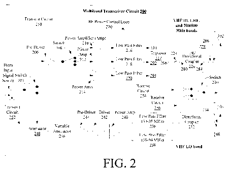
Referring now to FIG. 2, there is provided a schematic illustration of
an exemplary multiband transceiver 200 implemented in the communication device
100 of FIG. 1. The multiband transceiver 200 requires that multiple
transmitters be
connected to the antenna element 102 with a regulated output power. As such,
the
multiband transceiver 200 includes two (2) parallel transmit circuits 250, 252
and two
(2) parallel receive circuits 254, 256 connected to an antenna port 286. The
parallel
circuits 250, 253, 254, 256 provide a communication system that overcomes
certain
drawbacks of conventional communication systems. For example, conventional
communication systems comprising separate transceivers for each frequency band
is
more hardware intensive and expensive to implement than the multiband
transceiver
200 of the present invention.
Referring again to FIG. 2, a switch 204 is coupled to the two (2)
parallel transmit circuits 250, 252 and a switch 230 is coupled to the two (2)
parallel
receive circuits 254, 256. The switch 204 selectively couples an input signal
source
(not shown) to the transmit circuits 250, 252. For example, if a transmit
signal having
a frequency in the VHF Hi band is to be transmitted from the antenna element
102,
then the switch selectively couples the input signal source (not shown) to the
transmit
circuit 250. Similarly, if a transmit signal having a frequency in the UHF
band is to
be transmitted from the antenna element 102, then the switch selectively
couples the
input signal source (not shown) to the transmit circuit 250. Likewise, if a
transmit
signal having a frequency in the 700/800 MHz band is to be transmitted from
the
antenna element 102, then the switch selectively couples the input signal
source (not
-8-
CA 02761611 2011-11-09
WO 2010/141556 PCT/US2010/037031
shown) to the transmit circuit 250. If a transmit signal having a frequency in
the VHF
LO band is to be transmitted from the antenna element 103, then the switch
selectively couples the input signal source (not shown) to the transmit
circuit 252. It
should be noted that the present invention is not limited to the switch 230
and transmit
circuit 250, 252 configuration shown in FIG. 2. For example, the multiband
transceiver 200 can be absent of the transmit circuit 252. In such a scenario,
the
multiband transceiver 200 is also absent of the switch 230.
Each transmit circuit 250, 252 is generally configured to generate RF
electromagnetic energy and propagate RF electromagnetic signals with the aid
of the
antenna elements 102 and 103. Each receive circuit 254, 256 is generally
configured
to receive input signals from the antenna elements 102, 103 and forward these
signals
to subsequent processing devices (not shown). The subsequent processing
devices
(not shown) can include, but are not limited to, filters to separate a desired
radio
signal from all other signals picked up by the antenna elements 102 and 103,
amplifiers to amplify the desired radio signal's amplitude, and a conversion
device
(e.g., demodulators and decoders) to convert the desired radio signal into a
form (e.g.,
sound) usable for a user (not shown) of the communication device 100.
As shown in FIG. 2, the transmit circuit 250 is a multiband transmit
circuit that supports analog and digital communications in the following
bands: 136-
174 MHz VHF Hi band; 380-520 MHz UHF band; and 762-870 MHz band. As such,
the transmit circuit 250 requires that multiple transmit sub-circuits be
connected to the
antenna element 102 with a regulated output power. Each sub-circuit is
included in
an RF power control loop 270 configured to provide a substantially constant
power
over a wide range of frequencies at an input terminal of the antenna element.
Each
sub-circuit includes a plurality of power amplifiers 210, 212, 214 connected
in
parallel with each other and a plurality of low pass filters 216, 218, 220
connected in
parallel with each other. The RF power control loop 270 also comprises a
multiplexer
222, a diode 224 and a directional coupler 226. In the embodiment shown, the
multiplexer 222 is in the configuration of a triplexer, meaning that it has
three (3)
inputs and a single output. However, the invention is not limited in this
regard.
-9-
CA 02761611 2011-11-09
WO 2010/141556 PCT/US2010/037031
Notably, the inclusion of the triplexer 222 in the RF power control
loop 270 allows for the elimination of additional impedance matching circuits
and
harmonic filters from the transceiver design. As such, the implementation of
the
transceiver 200 of FIG. 2 is less expensive than the implementation of
conventional
transceivers. Also, the transceiver 200 is less hardware intensive than
conventional
transceivers, and therefore takes up a smaller amount of valuable space on
printed
circuit boards than conventional transceivers. Further, the power at an input
terminal
of the antenna element 102 is more constant and accurate as compared to the
power at
antenna elements of conventional communication devices combined for multiband
operation.
As shown in FIG. 2, a pre-driver 206 and switch 208 are coupled to the
RF power control loop 270. The switch 208 selectively couples the pre-driver
206 to
the power amplifiers 210, 212, 214. For example, if a transmit signal having a
frequency in the 136-174 MHz VHF Hi band is to be transmitted from the antenna
element 102, then the switch selectively couples the pre-driver 206 to the
power
amplifier 210. Similarly, if a transmit signal having a frequency in the UHF
band is
to be transmitted from the antenna element 102, then the switch selectively
couples
the pre-driver 206 to the power amplifier 212. Likewise, if a transmit signal
having a
frequency in the 700/800 MHz band is to be transmitted from the antenna
element
102, then the switch selectively couples the pre-driver 206 to the power
amplifier 214.
The pre-driver 206 and each power amplifier 210, 212, 214 provide a
gain chain that increases the power of transmit signals from a low value to a
high
value. Each of the low pass filters 216, 218, 220 passes low-frequency signals
and
attenuates (reduces the amplitude of) signals with frequencies higher than a
cutoff
frequency. The cutoff frequency of each low pass filter 216, 218, 220 is
selected in
accordance with a particular transmit application.
The triplexer 222 is generally composed of a passive circuit with three
(3) input terminals 290, 292, 294 that are isolated from each other and
combine to a
common output terminal 296. A schematic illustration of such an exemplary
passive
circuit 300 forming the triplexer 222 is shown FIG. 3. As shown in FIG. 3, the
-10-
CA 02761611 2011-11-09
WO 2010/141556 PCT/US2010/037031
passive circuit 300 includes a one hundred thirty six to one hundred seventy
four
Mega Hertz (136-174 MHz) input port (as shown by 290 of FIG. 3), a three
hundred
eighty to five hundred twenty Mega Hertz (380-520 MHz) input port and a seven
hundred sixty to eight hundred seventy Mega Hertz (760-870 MHz) input port. A
plot
of the triplexer's frequency response is provided in FIG. 4. As shown in FIG.
4, a
first trace 404 is provided which shows the low pass filter response of the
passive
circuit 300 for the 136-174 MHz band. The passband of the filter is
illustrated by
markers m20 and m2l of FIG. 4. The low pass filter response provides harmonic
rejection at the 2nd and higher order harmonic frequencies. The harmonic
rejection is
illustrated by markers m22 and m23 of FIG. 4. The low pass filter prevents
energy
from being transferred to the 380-520 MHz input port and the 760-870 MHz input
port. A second trace 406 is provided that shows the bandpass filter response
of the
passive circuit 300 for the 380-520 MHz band. The passband of the filter is
illustrated
by markers m16 and ml7 of FIG. 4. The bandpass filter response provides
harmonic
rejection at the 2nd and higher order harmonic frequencies. The harmonic
rejection is
illustrated at marker ml 8 of FIG. 4. The highpass section of the bandpass
filter
prevents energy from being transferred back into the 136-174 MHz input port
(as
shown by marker ml9 of FIG. 4). The low pass section of the bandpass filter
prevents energy from being transferred into the 760-870 MHz port (as shown by
marker ml 8 of FIG. 4). The third trace 408 is provided which shows the
bandpass
filter response of the passive circuit 300 for the 760-870 MHz band. The
passband of
the filter is illustrated by markers m13 and m14 of FIG. 4. The bandpass
filter
provide harmonic rejection at the 2nd and higher order harmonic frequencies
(no
marker is shown in FIG. 4 to illustrate the harmonic rejection). The highpass
section
of this bandpass filter prevents energy from being transferred back into 380-
520 MHz
input port (as shown by marker ml5 of FIG. 4) and 136-174 MHz input port.
Embodiments of the present invention are not limited to the passive circuit
design of
FIG. 3.
Referring again to FIG. 2, the triplexer 222 provides harmonic filtering
for each power amplifier 210, 212, 214. The triplexer 222 does not require
switching
-11-
CA 02761611 2011-11-09
WO 2010/141556 PCT/US2010/037031
to route signals from each of the input ports 290, 292, 294 to the common
output port
296. As such, the triplexer 222 provides a multiband transceiver with certain
advantages over various conventional transceivers. For example, if a
conventional
transceiver circuit implements complex switching circuits including PIN diodes
and/or RF relays (instead of a triplexer), then it requires relatively complex
software
and/or hardware for controlling the switching circuits. Consequently, the
conventional diode/relay based transceiver circuit is more expensive and
hardware
intensive as compared to the transceiver circuit 200 shown in FIG. 2.
Referring again to FIG. 2, the triplexer 222 is coupled to the directional
coupler 226 via a diode 224. The diode 224 prevents current from flowing
through
the triplexer 222 in a undesirable direction (i.e., a direction opposite a
transmit signal
propagation direction) during a transmit and/or receive mode. The directional
coupler
226 is configured to communicate a transmit signal to the antenna element 102
for
transmission therefrom. In this regard, the directional coupler 226 has an
input port
280 electrically connected to the common output port 296 of the multiplexer
and a
transmitted port 284 connected to an antenna port 286.
The directional coupler 226 is also configured to ensure that constant
power will occur at the antenna port 286. In this regard, the directional
coupler 226
provides a sample of RF power propagated in a particular direction (e.g., a
transmit
signal propagation direction) on a transmission line. This sample is provided
at
coupled port 282, and is used to provide a gain control signal. Gain control
signal is
communicated to a conversion circuit (not shown in FIG. 2). More particularly,
the
directional coupler 226 includes a coupled port 282 configured for coupling a
portion
of an RF signal to the conversion circuit (not shown). At the conversion
circuit (not
shown), the gain control signal is converted to a DC voltage signal. The DC
voltage
signal is then communication from the conversion circuit to each power
amplifier
210, 212, 214. Accordingly, each power amplifier 210, 212, 214 has a gain
control
terminal for receiving the DC voltage signal (or feedback signal). Each of the
power
amplifiers 210, 212, 214 is responsive to the DC voltage signal (or feedback
signal)
for maintaining a controlled power output at the antenna port 286 over a range
of
-12-
CA 02761611 2011-11-09
WO 2010/141556 PCT/US2010/037031
frequencies defined by two or more frequency bands. The gain control signal
can also
be communicated from the directional coupler to a processing device (not
shown)
and/or controller (not shown) for protecting the transceiver from any
impedance
mismatch. An exemplary embodiment of the directional coupler 226 will be
described in more detail below in relation to FIGS. 5-8.
As shown in FIG. 2, the transmit circuit 252 is a transmit circuit that
supports analog communications in the 30-50 MHz VHF LO band. As such, the
transmit circuit 252 is comprised of an attenuator 248, a variable attenuator
246, a
pre-driver 244, a driver 242, a power amplifier 240, low pass filters 236, 238
and a
directional coupler 232. The attenuators 248, 246 are generally configured to
reduce
the amplitude or power of an input signal without appreciably distorting its
waveform.
However, the variable attenuator 246 is driven by a control signal received
from the
directional coupler 232. The pre-driver 244, driver 242, power amplifier 240
provide
a gain chain that increases the power of transmit signals from a low value to
a high
value. Each of the low pass filters 236, 238 passes low-frequency signals and
attenuates (reduces the amplitude of) signals with frequencies higher than a
cutoff
frequency. The cutoff frequency of each low pass filter 236, 238 is selected
in
accordance with a particular transmit application.
Each low pass filter 236, 238 is coupled to the directional coupler 232
via a respective diode 262, 264. The diodes 262, 264 prevent current from
flowing
through the low pass filters 236, 238 in an undesirable direction during
transmit and
receive modes. The directional coupler 232 is configured to communicate a
transmit
signal to the antenna element 102 for transmission therefrom. The directional
coupler
232 provides a sample of the transmitted RF signal to a detector circuit (not
shown) to
generate a gain control signal. The gain control signal is communicated to the
variable attenuator 246, which has a control terminal for receiving the
control signal.
The control signal can be used to define an error voltage value to control
variable
attenuator 246 by comparing a sensed power value to a reference value. The
directional coupler 232 is also configured to measure reflected power from the
antenna element 102 to provide a measure of protection for the power
amplifiers from
-13-
CA 02761611 2011-11-09
WO 2010/141556 PCT/US2010/037031
impedance mismatch. An exemplary embodiment of the directional coupler 232
will
be described in more detail below in relation to FIGS. 5-8.
It should be understood that the present invention is not limited to the
embodiment shown in FIG. 2. For example, the transceiver 200 can be absent of
switch 204 and the transmit circuit 252. Also, the transmit circuit 250 can be
altered
so as to support analog communications in one or more additional bands, such
as the
VHF LO band. In the VHF LO band scenario, the transmit circuit 250 would
include
an additional transmit sub-circuit in the RF power control loop 270 and a
quadraplexer (instead of the triplexer 222).
Referring now to FIG. 5, there is provided a schematic illustration of
an exemplary directional coupler 500 that is useful for understanding the
present
invention. A schematic illustration of an equivalent circuit for the
directional coupler
500 is provided in FIG. 6. The directional couplers 226, 232 of FIG. 2 can be
the
same as or substantially similar to the directional coupler 500. As such, the
following
discussion is sufficient for understanding the directional couplers 226, 232
shown in
FIG. 2.
The directional coupler 500 ensures that constant output power will
occur at an antenna element (e.g., the antenna element 102 shown in FIGS. 1-2)
as
described above in relation to FIG. 2. In this regard, it should be understood
that the
directional coupler 500 is advantageously designed to provide a flat response
across
all frequency bands covered by a multiplexer (e.g., the multiplexer 222 shown
in FIG.
2). As such, a power at an input port of an antenna element is substantially
constant
throughout each frequency band and between multiple frequency bands. The
directional coupler 500 is also provided to facilitate the protection of a
transceiver
from any impedance mismatch as described above in relation to FIG. 2. The
directional coupler 500 is frequency scaled to cover frequencies selected in
accordance with a particular application. For example, the coupler 500 is
frequency
scaled to cover frequencies in the range of one hundred thirty six Mega Hertz
to eight
hundred seventy Mega Hertz (136-870 MHz) so as to accommodate P25 RF bands.
-14-
CA 02761611 2011-11-09
WO 2010/141556 PCT/US2010/037031
According to an aspect of the present invention, the directional coupler
500 is a multi octave surface mount directional coupler with improved coupling
flatness, directivity and insertion loss. The improved coupling flatness
facilitates a
more accurate power control. The improved coupling flatness also allows for
the
reduction or elimination of power control look up tables. The improved
directivity
provides a directional coupler with a more accurate Voltage Standing Wave
Ratio
(VSWR) cutback characteristic. The improved insertion loss provides a
transceiver
with an improved efficiency that extends the battery life thereof and reduces
thermal
heating with the transceiver.
The directional coupler 500 can be packaged in a small Surface Mount
Technology (SMT) package. The directional coupler 500 has a transformer
isolating
shield incorporated therein so as to improve performance thereof and minimize
the
amount of space it takes up on printed circuit boards. The transformer
isolating shield
will be described below. The directional coupler 500 overcomes certain
drawbacks of
conventional couplers. For example, the directional coupler 500 of the present
invention is less sensitive to winding placement as compared to conventional
couplers
having an SMT design and lacking shields to isolate transformers. In this
regard, it
should be understood that the winding placement at higher frequencies can
drastically
limit performance because the windings from the transformers can couple to
each
other. Also, the directional coupler 500 of the present invention has an
improved
broadband performance as compared to conventional couplers.
As shown in FIGS. 5-6, the directional coupler 500 is implemented
using a pair of coupled transformers 502, 504, a Printed Wiring Board (PWB)
514 and
wires 508, 512. The PWB 514 includes two (2) plated wells 516, 518. Each
plated
well 516, 518 is cavity plated on its sidewalls and bottom surface with a
particular
finish. The finish can include, but is not limited to, an Electroless Nickel
Immersion
Gold (ENIG) finish and a Hot Air Solder Leveling (HASL) finish. Each plated
well
516, 518 has a size and shape suitable for receiving a transformer 502, 504.
Each of the transformers 502, 504 is disposed within a respective one
of the plated wells 516, 518. The plated wells 516, 518 provide shields for
isolating
-15-
CA 02761611 2011-11-09
WO 2010/141556 PCT/US2010/037031
the transformers 502, 504 from each other and/or reducing electric field
coupling
between the transformers 502, 504. In this regard, it should be noted that
optimal
shielding is achieved by placing the primary and secondary windings (not shown
in
FIG. 5) of the transformers 502, 504 in the plated wells 516, 518. The wires
508, 512
are used to space the primary and secondary windings (not shown) from the
cores of
the transformer 502, 504. The wires 508, 512 are also used to couple the
transformers
502, 504 together. The wires 508, 512 can be, but are not limited to, wires
having a
TEFLON insulation. The directional coupler 500 can further include a shield
element or cover (not shown) placed on top of the transformers 502, 504 so as
to
enclose the transformers 502, 504 in the plated wells 516, 518.
As shown in FIG. 6, the directional coupler 500 includes four (4) ports
280, 282, 284 and 550. The ports 280, 282, 284 and 550 are designed to operate
at an
impedance (e.g., 50 Ohm impedance) selected in accordance with a particular
application. The input of a main line 610 is through the input port 280, while
the
output of this main line 610 is through the transmitted port 284. The input of
the
coupled line 612 is through coupled port 284, while the output of this coupled
line
612 is through isolated port 550. The primary winding 602 of the transformer
502 is
connected in series with the main line 610, while the primary winding 604 of
the
transformer 504 is connected in series with the coupled line 612. The primary
winding 602 is coupled to the secondary winding 606 of the transformer 502.
The
primary winding 604 is coupled to the secondary winding 608 of the transformer
504.
The secondary winding 602 of the transformer 502 is connected at one end to
ground
and at the other end to coupled port 282. The secondary winding 608 of the
transformer 504 is connected at one end to ground and at the other end to
transmitted
port 284.
In operation, a first signal propagated on the main line 610 at input port
280 is communicated to transmitted port 284. The first signal causes a second
signal
to be induced in the secondary winding 606 of the transformer 502. The second
signal is communicated from the secondary winding 608 to coupled port 282, and
therefore current for the second signal flows onto the coupled line 612. The
current
-16-
CA 02761611 2011-11-09
WO 2010/141556 PCT/US2010/037031
flow direction of the first signal in the primary winding 602 dictates the
current flow
direction of the second signal in the secondary winding 606. Therefore,
current for
the second signal will flow through the secondary winding 606 in a first
direction
when the first signal is placed on input port 280. In contrast, current for
the second
signal will flow through the secondary winding 606 in a second direction when
the
first signal is placed on transmitted port 284, where the second direction is
opposite
the first direction. A portion of the current for the first signal flows from
transmitted
port 284 through the secondary winding 608 of transformer 504 to ground. In
effect,
current for a third signal flows through the primary winding 604 of
transformer 504
onto the coupled line 612. The second and third signals are set to be nearly
equal to
each other. As a result, the second and third signals will add together when
current
for the first signal flows through primary winding 602 in the first direction.
The
second and third signals will cancel each other when current for the first
signal flows
through primary winding 602 in the second direction. Consequently, a signal
will be
output at isolated port 550 only when current for the first signal flows
through the
main through line 610 in the first direction.
An exemplary embodiment of a transformer 700 will now be described
in relation to FIGS. 7-10. The transformers 502, 504 of FIG. 5 can be the same
as or
substantially similar to the transformer 700. As such, the discussion of the
transformer 700 is sufficient for understanding the transformers 502, 504.
Referring now to FIG. 7, there is provided a top view of the
transformer 700. A side view of the transformer 700 is provided in FIG. 8. As
shown
in FIGS. 7-8, the transformer 700 is comprised of a toroidal core 706, a
primary
winding 704, and a secondary winding 702 with a shoulder washer 802 disposed
thereon. The shoulder washer 802 is used to space the primary winding 704 from
the
toroidal core 706. The toroidal core 706 can be selected in accordance with a
particular application. For example, the toroidal core 706 can be an RF
toroidal core
having a part No. T30-0 available from Micrometals, Inc. of Anaheim
California.
Embodiments of the present invention are not limited in this regard.
-17-
CA 02761611 2011-11-09
WO 2010/141556 PCT/US2010/037031
The primary winding 704 is wound at least one (1) turn around the
toroidal core 706. The primary winding 704 is formed of a coaxial cable having
a
desired impedance (e.g., a 50 Ohm impedance). The primary winding 704 can be
formed of a tin plated coaxial cable having a part number UT-070C-TP available
from
Micro-Coax, Inc. of Pottstown, Pennsylvania. Notably, the coaxial cable
includes a
center conductor and a shield. The center conductor is used to carry an RF
signal.
One side of the shield is coupled to ground to create a faraday shield around
the center
conductor. Embodiments of the present invention are not limited in this
regard.
The secondary winding 702 is wound N turns around the toroidal core
706, where N is an integer (e.g., 11). The secondary winding 702 can be formed
of
any wire other than Bi-Filiar wire. For example, the secondary winding can be
formed of a subminiature lead wire having a part number 28TDQ available from
Phoenix Wire, Inc. Embodiments of the present invention are not limited in
this
regard.
Method For Maintaining A Controlled Power Output At An Antenna Port
Referring now to FIG. 9, there is provided an exemplary method for
maintaining a controlled power output at the antenna port over a range of
frequencies
defined by two or more frequency bands. As shown in FIG. 9, the method 900
begins
at step 902 and continues with step 904. In step 904, an RF signal is
propagated along
any one of a plurality of parallel transmit paths of a multiband transceiver
in a
transmit propagation direction. The RF signal has a frequency falling within
one of
the following frequency bands 136-174 MHZ VHF Hi band, 380-520 MHz UHF band
and 762-870 MHz band. In a subsequent step 906, the RF signal is routed from
one
of a plurality of multiplexer input ports (e.g., input ports 290, 292, and 294
of FIG. 2)
to a common multiplexer output port (e.g., output port 296 of FIG. 2). Next, a
harmonic distortion is reduced in the RF signal. The harmonic distortion can
be
reduced using a multiplexer (e.g., the triplexer 22 of FIG. 2). Thereafter,
step 910 is
performed where feedback signal is generated. The feedback signal is generated
by
coupling a portion of the RF signal from the common multiplexer output port to
a
common feedback loop (e.g., the RF power control loop 270 of FIG. 2) for a
plurality
-18-
CA 02761611 2011-11-09
WO 2010/141556 PCT/US2010/037031
of transmit sub-circuits (e.g., transmit circuits 210/216, 212/218 and 214/220
of FIG.
2). In a next step 912, the feedback signal is provided to at least one of the
transmit
sub-circuits. The feedback signal is used in step 914 to maintain a controlled
power
output at an antenna port (e.g., the antenna port 286 of FIG. 2) over a range
of
frequencies defined by the two or more frequency bands. Next, step 916 is
performed
where the method 900 returns to step 902 or subsequent processing is resumed.
Applicants present certain theoretical aspects above that are believed to
be accurate that appear to explain observations made regarding embodiments of
the
invention. However, embodiments of the invention may be practiced without the
theoretical aspects presented. Moreover, the theoretical aspects are presented
with the
understanding that Applicants do not seek to be bound by the theory presented.
While various embodiments of the present invention have been
described above, it should be understood that they have been presented by way
of
example only, and not with limitation. Numerous changes to the disclosed
embodiments can be made in accordance with the disclosure herein without
departing
from the spirit or scope of the invention. Thus, the breadth and scope of the
present
invention should not be limited by any of the above described embodiments.
Rather,
the scope of the invention should be defined in accordance with the following
claims
and their equivalents.
Although the invention has been illustrated and described with respect
to one or more implementations, equivalent alterations and modifications will
occur to
others skilled in the art upon the reading and understanding of this
specification and
the annexed drawings. In addition, while a particular feature of the invention
may
have been disclosed with respect to only one of several implementations, such
feature
may be combined with one or more other features of the other implementations
as
may be desired and advantageous for any given or particular application.
The terminology used herein is for the purpose of describing particular
embodiments only and is not intended to be limiting of the invention. As used
herein,
the singular forms "a", "an" and "the" are intended to include the plural
forms as well,
unless the context clearly indicates otherwise. Furthermore, to the extent
that the
-19-
CA 02761611 2011-11-09
WO 2010/141556 PCT/US2010/037031
terms "including", "includes", "having", "has", "with", or variants thereof
are used in
either the detailed description and/or the claims, such terms are intended to
be
inclusive in a manner similar to the term "comprising."
The word "exemplary" is used herein to mean serving as an example,
instance, or illustration. Any aspect or design described herein as
"exemplary" is not
necessarily to be construed as preferred or advantageous over other aspects or
designs. Rather, use of the word exemplary is intended to present concepts in
a
concrete fashion. As used in this application, the term "or" is intended to
mean an
inclusive "or" rather than an exclusive "or". That is, unless specified
otherwise, or
clear from context, "X employs A or B" is intended to mean any of the natural
inclusive permutations. That is if, X employs A; X employs B; or X employs
both A
and B, then "X employs A or B" is satisfied under any of the foregoing
instances.
-20-