Note: Descriptions are shown in the official language in which they were submitted.
CA 02761962 2011-11-15
WO 2010/135689 PCT/US2010/035836
MINI-EXTRUSION MULTILAYERING TECHNIQUE FOR THE FABRICATION OF
CERAMIC/PLASTIC CAPACITORS WITH COMPOSITION-MODIFIED BARIUM
TITANATE POWDERS
BACKGROUND
Capacitors have long been used to build circuits. In particular, capacitors
have been
used in energy circuits to decouple DC voltage from AC current. In other
examples,
capacitors have been used in electronic circuits to provide desired circuit
responses and
functions. More recently, large capacitors have been proposed as energy
storage devices.
Previously, single-layer capacitors, including electrodes located on ether
side of a
single dielectric layer, have been formed through screen-printing processes.
Such processes
generally include printing a layer through a mask and baking the layer prior
to adding a
second layer. While such processes can be acceptable for single-layer
capacitors, screen
printing is inefficient for multiple-layer capacitors.
To form a multiple-layer capacitor, screen-printing techniques would lead to a
large
number of repetitive baking steps, each involving heating, treatment, and
cooling periods that
add time and expense to the production process. As such, screen-printing
techniques have
proven less desirable for forming multilayer capacitors and in particular,
capacitive storage
devices.
BRIEF DESCRIPTION OF DRAWINGS
The present disclosure may be better understood, and its numerous features and
advantages made apparent to those skilled in the art by referencing the
accompanying
drawings.
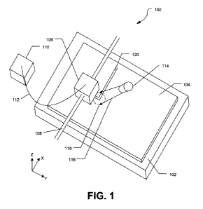
FIG. 1 includes an illustration of an exemplary continuous printing device.
FIG. 2 includes a flow diagram illustrating an exemplary method of forming a
capacitive storage device.
FIG. 3, FIG. 4, and FIG. 5 include illustrations of exemplary layers of a
capacitive
storage device.
FIG. 6 includes an illustration of an exemplary nozzle configuration.
-1-
CA 02761962 2011-11-15
WO 2010/135689 PCT/US2010/035836
FIG. 7 includes an illustration of an exemplary deposition pattern.
FIG. 8 includes an illustration of a cross-section of an exemplary layered
construction.
FIG. 9 includes an illustration of an exemplary deposition pattern.
FIG. 10 and FIG. 11 include illustrations of exemplary nozzles.
The use of the same reference symbols in different drawings indicates similar
or
identical items.
DETAILED DESCRIPTION
In a particular embodiment, a set of inks are deposited in patterned layers to
form a
component of a capacitive energy storage device. An exemplary ink includes
conductive
particulate and can be used to form electrode. Another exemplary ink includes
dielectric
ceramic particulate and a polymer powder and can be used to form dielectric
layers. A further
exemplary ink includes a polymer powder and can be deposited around electrodes
and
dielectric layers within patterned layers. In a further embodiment, the inks
can each be
deposited from a print head in continuous streams to form elements of the
component.
In an exemplary embodiment, a continuous printing apparatus, such as laminar-
flow
printing device, can be used to form layers of a capacitive storage device.
For example, FIG.
1 includes an illustration of an exemplary printing apparatus 100. A work
piece support 102
supports and retains a work piece 104. The work piece 104 can be a portion of
a multilayer
capacitor or can be a poly(ethylene terephthalate) (PET) film or a paper
support on which a
multilayer capacitor work piece can be initiated. The work piece 104 can be
held in place by
clamps or pins, by an adhesive film, by vacuum, electrostatically, or any
combination
thereof. Alternatively, the work piece support 102 can be coated with
polytetrafluoroethylene
(PTFE) plastic, and a first layer of polymer, such as poly(ethylene
terephthalate) (PET), can
be printed directly upon the work piece support 102.
In addition, the printing apparatus 100 includes a print head assembly 106 and
a print
head support 108. In general, the print head assembly 106 is configured to
deliver an ink or
suspension from a nozzle to the work piece 104 in a continuous flow, such as a
laminar flow.
In contrast to other printing techniques, ink is delivered in a continuous
stream instead of
periodic or discrete dots or extrusion through a masked screen. In an example,
the print head
assembly 106 can be configured to deliver a single stream of ink or of a
suspension. In
-2-
CA 02761962 2011-11-15
WO 2010/135689 PCT/US2010/035836
another example, the print head assembly 106 can be configured to deliver the
ink or
suspension in two or more continuous streams, such as at least two, at least
three, at least four,
or at least eight streams. For example, the print head assembly 106 can
include one or more
nozzles, each controllable to deliver ink in continuous streams, such as
laminar streams.
In a further embodiment, the print head assembly 106 can be configured to
deliver a
single ink or suspension. Alternatively, the print head assembly 106 can be
configured to
selectively deliver two or more inks or suspensions. For example, two or more
feed lines can
provide two or more ink compositions to the print head assembly 106, and the
print head
assembly 106 can be configured to selectively or controllably deliver one or
more of the ink
compositions to the work piece 104. In an example, the print head assembly 106
can be
configured to deliver streams of two or more inks simultaneously while in
relative motion in
relation to the work piece 104.
In an example, the printing apparatus 100 can include one or more containers
110 that
are fluidly coupled to the print head assembly 106 via a feed line or feed
lines 112. The feed
lines 112 provide one or more inks or suspensions from the container 110 to
the print head
assembly 106. In an embodiment, more than one feed line 112, more than one
container 110,
or any combination thereof can be connected to the print head assembly 106.
Ultrasonic
agitation of the ink can be provided to the ink in the container 110 or at a
reservoir close to
the nozzle of the printing process to assure complete dispersion of the
particulate components.
A reservoir associated with inks to be dispensed for forming polymeric layers
can be
kept at a pressure of 20 psi to 100 psi and a temperature in a range of 20 C
to a 50 C. For
the larger or thicker polymeric layers, the reservoir pressure can be held at
20 psi to 100 psi.
For reservoirs associated with the dispensing of dielectric powders or layers,
the
reservoir can be held at a pressure of 20 psi to 100 psi at a temperature of
20 C to 50 C. A
reservoir associated with nozzles for printing conductive layers can be held
at a pressure of 10
psi to 70 psi and a reservoir temperature of 20 C to 50 C.
Optionally, the printing apparatus 100 can include at least one energy source
114.
For example, the energy source 114 can be a radiative source, such as an
ultraviolet source, a
visible light source, an infrared source, or a combination thereof. In
particular, the radiative
source can be an infrared heat source, such as a source of electromagnetic
energy in the
frequency range of between about 1.2x10¹⁴ Hz and 1.5x10¹³ Hz. In a further
example, the
energy source 114 can be in the form of a reflected diffuse light or can be a
laser source. In
an example, the energy source 114 directs energy 116, such as infrared
radiation, to impinge
-3-
CA 02761962 2011-11-15
WO 2010/135689 PCT/US2010/035836
upon at least a portion 118 of the work piece 104 in proximity to the ink
dispensed from the
print head assembly 106. In an example, the energy source 114 can move with
the print head
assembly 106 or the direction of the energy 116 can be adjusted to follow the
movement of
the print head assembly 106 or work piece 104.
In particular, the work piece support 102 or the print head assembly 106, or
both are
configured to create motion relative to each other, effectively altering the
position at which a
continuous stream is deposited on to the work piece 104. As a result, a
continuous layer 120
is printed on the work piece 104. Depending on the relative motion of the
print head
assembly 106 and the work piece 104, the layer 120 can be straight, curved, or
include sharp
angles. In a particular example, the work piece support 102 can be configured
to move in one
or more of an x- or y-direction relative to a planar surface formed by the
work piece support
102. In another example, the print head assembly 106 can be configured to move
in one or
more of an x- or y-direction. In a further example, the work piece support 102
can be
configured to move in a first direction, such as an x-direction or a y-
direction, and the print
head assembly 106 can be configured to move in a second direction, such as a y-
direction or
an x-direction. One or both of the work piece support 102 or the print head
assembly 106 can
be configured to move in the z-direction.
In a particular example, the print head assembly 106 is connected to an upper
stationary stainless steel platen of the printing system 100. More than one
print head 106 can
be coupled to the upper platen. The support 102 moves relative to the print
head or heads 106.
The number of print head assemblies can be set to provide the product
throughput desired
since each print head assembly prints layers for individual capacitors
simultaneously with the
other print head assemblies. However, printing-system size is a factor, so the
number of
layering print head assemblies can be limited by a practical printing-system
size as related to
manufacturing space limitations. The printing-system lower plate or support
102 is controlled
by the printing-system's xyz sled so that the nozzles can be in the proper
location, have the
proper height between the nozzle and the lower plate, and traverse at the
proper speeds during
the layering printing process. The platens are coated with a Teflon
fluorocarbon resin or any
suitable mold-release film or a thin layer of Mylar , poly(ethylene
terephthalate) film adhered
to the platen surface. The controller of the printing unit ensures that the
processing tanks are
at the specified temperature and pressure and process parameters as indicated
above are
completed as specified during the layering process. At the beginning of the
printing process
the printing unit automatically transports the coated or PET layered stainless
steel platen into
the unit and locks it into the proper printing location. At the end of the
printing process, the
printing unit automatically transports the stainless steel platen with the
layered capacitor
-4-
CA 02761962 2011-11-15
WO 2010/135689 PCT/US2010/035836
components out of the unit onto a transporting unit so that the components can
be processed
through the next stage of manufacturing. Layered thicknesses, lengths, and
widths that are
controlled by the extruder slits and the other processing parameters can be
varied to meet the
specifications of the particular application.
Exemplary parameter-setting capabilities and process setting for such
parameters can
be utilized to achieve successful extruding of the layer thicknesses
indicated. For example,
desired layer thickness can be controlled by varying the reservoir
temperatures, varying the
viscosity of the inks, adjusting the extruder silt widths, setting the
pressure in the processing
tanks, setting the height of the nozzle from the deposition platen surface,
setting the speed of
the nozzle in relationship to the deposition platen, setting the width of the
nozzle slit and
length of the layering process to establish the size of the capacitors,
varying the layer curing
temperature and air velocity, or any combination thereof.
In a particular embodiment, a continuous flow device can be used in
conjunction with
embodiments of inks and suspensions describe below to form multilayer
capacitors. For
example, FIG. 2 includes a flow diagram illustrating an exemplary method of
forming a
capacitive element. As illustrated at 202, a work piece can be placed on a
work piece
support. To initiate the formation of the multilayer capacitor, the work piece
can include a
polymer film or a paper. Alternatively, the work piece support can be coated
with
polytetrafluoroethylene (PTFE) plastic, and a first layer of a polymer, such
as poly(ethylene
terephthalate) (PET), can be printed directly upon the work piece support. For
example, a
layer can be printed with an ink or suspension including solvents or polymeric
binders in the
amounts described below, absent electrically conductive or dielectric ceramic
materials.
As illustrated at 204, a first electrode layer can be printed upon the work
piece. The
first electrode layer can be an anode layer or a cathode layer. In particular,
the first electrode
layer can be printed with an ink or suspension including an electrically
conductive particulate
such as aluminum, copper, nickel, tin or a combination of these electrically
conductive
particulate. For example, the ink or suspension can include one or more
solvents, a burn-out
binder, and an electrically conductive particulate. As the ink or suspension
is deposited, the
composition can form a conductive layer that can act as an electrode. In an
example, the first
electrode layer can have a thickness of between about 1 m to about 11 m. In
particular, the
ink or suspension is delivered in one or more continuous streams that are
concurrently
solidified.
Optionally, an insulative layer formed from an ink or suspension including
solvents
and burn-out organic binder with a dielectric polymeric particulate can be
printed to surround
-5-
CA 02761962 2011-11-15
WO 2010/135689 PCT/US2010/035836
the first electrode layer on at least three sides within the plane of the
electrode layer.
Alternatively, an insulative layer formed from an ink or suspension including
solvents and
burn-out polymeric binder with a dielectric glass particulate can be printed
to surround the
first electrode layer within the plane of the electrode layer. In a particular
embodiment, the
material of the electrode layer can be printed concurrently with at least a
portion of the
material of the insulative layer. Concurrently is used herein to indicate that
events can occur
simultaneously, can overlap in time, or one event can begin when another event
is ending.
As illustrated at 206, a first dielectric layer can be printed over the first
electrode
layer. The first dielectric layer can be printed with an ink or suspension
including a dielectric
particulate. For example, the ink or suspension can include solvents, a burn-
out binder (e.g., a
cellulose-based binder), and a dielectric particulate material, which when
deposited forms a
dielectric material layer. The dielectric particulate material can include
dielectric ceramic
material. In an example, the first dielectric layer can have a thickness of
between about 1 m
to about 11 m. In particular, one or more continuous streams of the
dielectric ink can be
printed and concurrently solidified to from the dielectric material layer.
Optionally, an
insulative layer formed from an ink or suspension including solvents and burn-
out organic
binder, absent particulate filler, but having a dielectric polymeric
particulate, can be printed to
surround the first dielectric layer on four sides within the plane of the
dielectric layer. In an
example, the dielectric material layer can be printed concurrently with at
least a portion of the
insulative layer.
As illustrated at 208, a second electrode layer can be printed upon the first
dielectric
layer. As with the first electrode layer, the second electrode layer can be
printed with an ink
or suspension including an electrically conductive particulate. For example,
the second
electrode layer can be formed from an ink or suspension similar to that used
to form the first
electrode layer or can be formed from a different ink or suspension. Depending
on the first
electrode layer, the second electrode layer can be a cathode layer or an anode
layer. For
example, when the first electrode layer is an anode layer, the second
electrode layer can be a
cathode layer. The second electrode layer can have a thickness of between
about 1 m to
about 11 m. In a particular embodiment, the second electrode layer can be
offset relative to
the first electrode layer to permit separate electrical connection, such as
separate electrical
connection on opposite sides of the capacitive element. Optionally, an
insulative layer
formed from an ink or suspension including solvents and polymeric binder,
absent ceramic
filler, but having a dielectric polymeric particulate, can be printed to
surround the second
electrode layer on at least three sides within the plane of the electrode
layer. In an example,
the electrode layer can be printed concurrently with at least a portion of the
insulative layer.
-6-
CA 02761962 2011-11-15
WO 2010/135689 PCT/US2010/035836
Further, as illustrated at 210, a second dielectric layer can be printed upon
the second
electrode layer. The second dielectric layer can be printed with an ink or
suspension
including a dielectric particulate. The second dielectric layer can be formed
from an ink or
suspension similar to that used to form the first dielectric layer or can be
formed from a
different ink or suspension. In an example the second dielectric layer can
have a thickness of
between about 1 m to about 11 m. Optionally, an insulative layer formed from
an ink or
suspension including solvents and polymeric binder, absent particulate filler,
but having a
dielectric polymeric particulate, can be printed to surround the second
dielectric layer on four
sides within the plane of the dielectric layer. In an example, the second
dielectric layer and at
least a portion of the insulative layer can be printed concurrently.
To form a multilayer capacitive element, the layering process can be repeated.
Returning to 204, an additional electrode layer can be printed over the second
dielectric
layer. In an embodiment, the process can be repeated until at least about 500
layers are
printed, and preferably at least about 1000 layers are printed, such as at
least about 2000
layers.
In an exemplary embodiment, the layers are printed with a stream printer. As
the ink
is deposited, it can be heated by an energy source, such as an infrared energy
source. Heating
the ink as it approaches a work piece can evaporate a portion of the solvent,
increasing the
viscosity of the ink before it contacts the work piece. The increased
viscosity can reduce the
spread of the ink and variations in the thickness of the layer. Additionally,
the energy source
can remove portions of binder from the layer by thermal decomposition.
Further, the energy
source can sinter other portions of the binder. In an embodiment, the energy
source can
provide sufficient energy to sinter the layer, increasing the density of the
layer at least about
75%, preferably at least about 85%, such as at least about 95%. In particular,
the heat
generated by the energy source is not sufficient to degrade the permanent
polymer binder or
the dielectric polymer particulate.
Alternatively, a gas, such as a hot gas can be directed over the deposited
layers to
evaporate solvent and decompose burn-out binders. For example, the gas can be
clean dry air,
nitrogen, or a noble gas. The gas can be heat to a temperature of 50 C to 150
C.
In addition to or alternatively, the capacitive element can be heat treated or
further
heat treated after a plurality of layers, such as after substantially all the
layers, are printed, as
illustrated at 212. In particular, the capacitive element can be hot
isostatically pressed, such
as at a pressure of at least 80 bar, for example, between 80 bar and 120 bar.
The temperature
can be at least about 150 C, preferably at least about 165 C, such as between
about 165 C
-7-
CA 02761962 2011-11-15
WO 2010/135689 PCT/US2010/035836
and about 215 C, or between about 170 C and about 200 C. Alternatively, when
the
dielectric material includes a vitreous coating or when a vitreous glass
insulation material is
used, the temperature can be at least about 400 C, such as at least about 500
C, at least about
700 C or even, at least about 900 C.
Further, the capacitive element can be cut, as illustrated at 214, and
electrical
connections applied to the electrodes, as illustrated at 216. For example,
when the cathodes
are offset from the anodes, as described above in relation to the first and
second electrode
layers, a single connection can be applied to a first side of the capacitive
element to connect
the cathodes, and a single connection can be applied to a second side of the
capacitive
element to connect the anodes. For example, the first and second sides can be
dipped in a
bath of molten metal. Alternatively, electrical connections can be established
with a
conductive adhesive.
Optionally, the multilayer capacitive element can be polarized, as illustrated
at 218.
For example, the capacitive element can be heated to a temperature of at least
about 150 C,
preferably at least about 165 C, such as between about 165 C and about 215 C,
or between
about 170 C and about 200 C. In addition, a voltage difference of at least
2000 V, such as at
least 3000 V, or even at least 3750 V is applied between the anodes and
cathodes after
heating.
Further, the multilayer capacitive elements can be packaged into a capacitive
storage
device, as illustrated at 220. For example, more than one capacitive element
can be
electrically coupled and secured in a single physical arrangement to form a
capacitive storage
device. In particular, several capacitive elements can be placed in a housing
that includes
electrical contacts that couple the capacitive elements in parallel or serial
arrangements, or
combinations thereof, to form the capacitive storage device.
In an exemplary embodiment, the above method and printing device can be used
to
form patterned layers of elements of a capacitive storage device. Patterned
layers describe the
nature of each layer including within the layer a pattern of deposited
materials. Patterned
layers are deposited on top of one another to form capacitive elements of the
capacitive
storage device. For example, FIG. 3, FIG. 4, and FIG. 5 include illustrations
of adjacent
layers of a multilayer energy storage device. As used herein, longitudinal
refers to the longest
orthogonal dimension of a layer, transverse refers to the second longest
orthogonal dimension
and thickness refers to the third longest orthogonal dimension. For example,
FIG. 3 includes
an illustration of an exemplary electrode layer (e.g., an anode layer), FIG. 4
includes an
illustration of an exemplary dielectric layer, and FIG. 5 includes an
illustration of an
-8-
CA 02761962 2011-11-15
WO 2010/135689 PCT/US2010/035836
exemplary opposite electrode layer (e.g., a cathode layer). As illustrated at
FIG. 3, within the
electrode layer, an electrode 302 is surrounded by an insulative portion 304,
such as a
dielectric polymeric portion. Alternatively, the dielectric polymeric portion
304 can be
substituted with a vitreous glass portion. In particular, the electrode 302
extends from a first
end 310 of the electrode layer to a position 306 that is spaced apart from the
second end 308
of the electrode layer. As illustrated, the electrode 302 forms a rectangular
shape that is
surrounded on three sides by the insulative portion 304. Such an electrode
layer can be
formed using variations on the nozzle arrays described below.
As illustrated at FIG. 4, a dielectric layer includes a dielectric ceramic
portion 412
surrounded by an insulative portion 414, such as a dielectric polymer portion,
on four sides.
The dielectric ceramic portion 414 can be disposed over a portion of the
underlying electrode
302. Further, the dielectric ceramic portion 412 is spaced away from the edges
308 and 310
of the layers. Alternatively, the dielectric polymer portion 414 can be
replaced with a
vitreous glass portion. As above, such a dielectric ceramic layer and the
associated dielectric
ceramic portion 412 and insulative portion 414 can be printed using variations
on the nozzle
arrays described below.
As further illustrated in FIG. 5, a second electrode 516 can be printed within
a layer
and can be surrounded on three sides by an insulative portion 518, such as a
dielectric
polymer portion. The second electrode 516 can contact the edge 308 and can be
spaced from
the edge 310 in contrast to the first electrode 302. As such, the second
electrode 516 is offset
from the first electrode 302. Alternatively, the dielectric polymer portion
518 can be replaced
with vitreous glass portion. Here too, the second electrode 516 and the
dielectric polymer
portion 516 can be formed using variations of the nozzle arrays described
below.
The multiple-layer capacitor configuration illustrated in FIG. 3, FIG. 4 and
FIG. 5 can
be utilized in the fabrication of capacitors for an energy-storage device. For
example, the
patterned layers can be printed using a single print head. Alternatively, more
than one print
head can be used. An exemplary print head is illustrated in FIG. 6. In
particular, the
patterned layers can be printed using continuous streams that are initiated
and stopped based
on position of the print head relative to the support. The layering in
relation to the printing
process, turn on and turn off timing of the valves, motor stopping signals is
illustrated in FIG.
7. An exemplary cross-sectional view of the resulting layers is illustrated in
FIG. 8.
Capacitive devices can be formed by placing conductive end caps, such as
copper end caps on
the capacitive elements once cut along the cut lines indicated in FIG. 7.
-9-
CA 02761962 2011-11-15
WO 2010/135689 PCT/US2010/035836
FIG .6 includes an illustration of an exemplary nozzle configuration 600. The
nozzle
configuration 600 is configured to print layers of the capacitive elements as
the print head
moves back and forth in the direction indicated at 602. The longitudinal
direction is parallel
to the direction 602 and transverse refers to the second longest orthogonal
dimension within a
plane parallel the print head. For example, nozzle A can be configured to
dispense an ink to
form a polymeric layer. Nozzle B can be configured to dispense an ink to form
a conductive
layer. Nozzle C can be configured to dispense ink to form a polymeric layer
and Nozzle D
can be configured to dispense an ink for forming a dielectric layer. Nozzles E
and F can
dispense clean dry gas such as air, nitrogen, or a noble gas.
In an example, nozzle A has a slit width in a range of 1.4 mils to 4 mils.
Nozzle C
has a slit width in a range of 4 mils to 8 mils, and nozzle D has a slit width
in a range of 4
mils to 8 mils. Nozzle B can have a slit width in a range of 1.4 mils to 4
mils. The speed of
the print head is in a range of 10 to 20 inches per second.
In particular, nozzle A and nozzles C are configured to dispense an ink that
forms a
polymeric layer. For example, nozzle A can dispense an ink to form polymeric
layers at the
planer ends of an electrode. In particular, nozzle A can be configured to
dispense ink
sufficient to form a polymeric end cap of equal thickness to the conductive
layer forming the
electrode. For example, the nozzle A can be configured to dispense sufficient
ink to form a
polymeric layer of thickness in a range of 0.5 microns to 3 microns, such as
0.5 microns to 2
microns, or 0.5 microns to 1.5 microns, or approximately 1 micron. While the
nozzles C are
configured to dispense a similar ink, the nozzle C can dispense enough ink
sufficient to form
a polymeric layer having a thickness of both a dielectric layer and a
conductive layer. For
example, if the dielectric layer is 10 microns and the conductive layer is 1
micron, the nozzle
C can dispense sufficient ink to form an 11 micron polymeric layer. In
particular, the nozzle
C can be configured to dispense ink to form a layer in a range of 9 to 15
microns, such as a
range of 9 to 12 microns, or even a range of 10 to 12 microns.
In a particular example, nozzles A and C are configured for the layering a
resin
powder, for example, poly(ethylene terephthalate) plastic (PET), within a
binder solution
which includes either a mixture of polypropylene carbonate (binder), and
acetone (solvent) or
solvents such as hexafluoro-2-propanol or 60/40 phenol/tetrachloroethylene.
The
concentration levels of the materials in the case of PET with either of the
solvents can be
varied to establish the appropriate viscosity for the layering or printing
process.
Nozzle B is configured to dispense an ink to form a conductive layer useful as
an
electrode of the capacitive elements. For example, the operation of nozzle B
can be
-10-
CA 02761962 2011-11-15
WO 2010/135689 PCT/US2010/035836
configured to dispense ink to form conductive layers of thickness in a range
of 0.5 microns to
3 microns, such as 0.5 microns to 2 microns, or even 0.5 microns to 1.5
microns, such as
approximately 1 micron.
In particular, nozzle B can be used for the layering of an electrical-
conducting-
particulate containing ink. The ink may or may not include a binder solution
of
poly(propylene) carbonate. In another example, acetone can be used in both
cases. The
viscosity of this ink can be established by varying the concentrations of the
constituents.
Nozzle D can be configured to dispense ink to form a dielectric layer. In an
example,
the nozzles D can be configured to dispense ink sufficient to form a
dielectric layer having a
thickness in a range of 8 to 15 microns, such as a range of 9 to 12 microns,
or even a range of
9 to 11 microns, such as approximately 10 microns.
In a particular example, for the layering of the ceramic powder, for example,
composition-modified barium titanate powder in a matrix of poly(ethylene
terephthalate), the
constituents are mixed with either a binder solution of poly(propylene)
carbonate and acetone
or solvents such as hexafluoro-2-propanol or 60/40 phenol/tetrachloroethylene,
and are
layered using the nozzle D. The concentration levels of the four materials or
two materials in
the case of PET with either of the solvents can be varied to establish the
appropriate viscosity
for the layering or printing process.
In particular, the nozzles can be controlled to dispense at particular times
and at
particular positions in conjunction with movement of the print head. When the
print head is
moving, the relative initiation of ink dispensing can result in the formation
of layers of
desired thickness and composition. For example as illustrated in FIG. 7, the
nozzles can be
turned on and off as the print head moves between position 1 and position 10
to print a series
or set of layers of a conductive or capacitive device, for example,
illustrated in FIG. 8.
Starting at position 1 illustrated at FIG. 7, the nozzle A can be turned on at
position 2
and turned off at position 4 and nozzle B can be turned on at position 4 and
turned off at
position 8. The motor controlling the print head can be turned off at position
9 and the print
head stopped at position 10. As a result, a first electrode layer 802 is
formed. A reverse pass
can be utilized to form the dielectric layer 804 and polymer layers 806 and
808. For example,
going in reverse starting at position 10, nozzles C and D can be turned on at
position 9 and off
at position 3 and the motor controlling the print head turned off at position
2 and the print
head stopped at position 1.
-11-
CA 02761962 2011-11-15
WO 2010/135689 PCT/US2010/035836
A subsequent electrode layer 810 can be deposited over the dielectric layer
804
utilizing a further forward pass starting at position 1. The nozzle B can be
initiated at position
2 and turned off at position 6 and the motor can be turned off at position 9
and the print head
stopped at position 10. Such a pass forms the conductive portion of an
electrode layer 810
offset from the electrode layer 802.
An additional dielectric layer 812, a portion of the conductive layer 810, and
polymeric layers 814 and 816 can be formed in a reverse pass starting at
position 10. For
example, nozzle A can be turned on at position 9 and turned off at position 7
forming a
polymeric portion of the electric layer 810. The nozzles C and D can be turned
on at position
9 and off at position 3 forming a dielectric layer 812 and sides of polymer
layers 814 and 816.
In an example, the driver of the print head is turned off at position 2 and
the print head is
stopped at position 1.
Prior to forming the structure illustrated in FIG. 8, full layers of polymeric
material
(e.g., 818, 820, and 822) can be formed using nozzles A and C. For example,
nozzle A can be
used to dispense multiple passes of a polymeric layer adding to an equivalent
thickness as the
layers dispense by nozzle C. Alternatively, the control rate flowing through
nozzles A and C
can be manipulated so that nozzles A and C dispense a polymer layer having
uniform
thickness.
The process of forming the interlaced dielectric and conductive layers can be
repeated
many times to form a capacitive element useful in capacitive energy storage
devices. For
example, the process can be repeated at least 100 times, such as at least 500
times, at least 800
times, or even at least 1000 times. While not illustrated in FIG. 7, a roller
can traverse behind
or in front of the print head to reduce voids within the layers. In an
example, the roller is
applied over the structure after deposition of each layer. Alternatively, the
roller can be
applied after deposition of more than one layer, such as every four layers.
While FIG. 7 illustrates a four pass method of depositing layers, alternative
methods
including more or fewer steps can be envisaged. For example, as illustrated in
FIG. 9, a first
pass can include turning nozzle B on at position 4 and off at position 8. With
each forward
pass, the print head is stopped at position 10. In a second pass, in a
direction opposite the first
pass, a nozzle C can be turned on at position 9 and off at position 3. With
each reverse pass,
the print head is stopped at position 1. In a third pass, the nozzle A is
turned on at position 2
and off at position 4. In a fourth pass, the nozzle D is turned on at position
9 and off at
position 3. In a fifth pass, the nozzle B is turned on at position 2 and off a
position 6. In a
sixth pass, the nozzle A is turned on at position 9 and off at position 7. In
a seventh pass, the
-12-
CA 02761962 2011-11-15
WO 2010/135689 PCT/US2010/035836
nozzle C is turned on at position 3 and off at position 9. In an eighth pass,
the nozzle D is
turned on at position 9 and off at position 3. The process can be repeated to
form additional
capacitive elements. In addition, layers of polymer material can be printed
before or after
printing of the capacitive elements.
In a particular example, FIG. 10 includes an illustration of an exemplary
nozzle
useful for dispensing inks to form polymeric layers, conductive layers, and
dielectric layers.
For example, the nozzle 1000 includes a solution inlet tubing 1002 and a
horizontal manifold
1004. A slit can be formed 1006 to dispense films forming the layers. Both
ends of the
manifold can be capped, resulting in ink being dispensed from the slit 1006.
To dispense gas useful in evaporating the solvent, nozzles E and F illustrated
in FIG.
6 can utilize a gas nozzle as illustrated in FIG. 11. For example, the gas
nozzle 1100 includes
a gas inlet tube 1102 feeding a manifold 1104. The end caps of the manifold
1104 can be
closed. On a bottom surface of the manifold 1104, a plurality of outlet holes
1108 can be
provided. In an example, the outlet holes have a diameter in a range of 1/64"
to 1/8". In a
particular example, in the clean dry gas dispensed from the nozzle 1100 has a
temperature in a
range of 50 C to 150 C.
Each of the inks includes a solvent and optionally a binder. In an exemplary
embodiment, the solvent can be a polar organic solvent, including, for
example, an alcohol
such as propyl alcohol or isopropyl alcohol; a ketone such as methyl ethyl
ketone or acetone;
a glycol such as ethylene glycol, 1,2-propylene glycol, 1,3-propylene glycol,
or diethylene
glycol; a glycol ether such as diethylene glycol monoether, ethylene glycol
butyl ether,
diethylene glycol monobutyl ether, dipropylene glycol monomethyl ether, or
ethylene glycol
monoethyl ether; glycerol (glycerine or 1,2,3-propanetriol); an ester; an
aldehyde; or any
combination thereof. Alternatively, the solvent can be a nonpolar organic
solvent including,
for example, aliphatic hydrocarbons, such as hexane or mixed alkanes, or
aromatic
hydrocarbons, such as benzene or toluene.
In a further exemplary embodiment, the ink can include more than one solvent.
For
example, the ink can include a first solvent and a second solvent. The first
solvent can be a
solvent having a boiling point in a first range of temperatures, and the
second solvent can be a
solvent having a boiling point in a second range of temperatures, such as a
range of
temperatures higher than the first range of temperatures. As a result, the
rate of evaporation
of the first solvent can be higher than the rate of evaporation of the second
solvent at a given
temperature. Accordingly, the viscosity of the ink can change as the first
solvent is
evaporated, while providing a desirable rheology. In particular, the
difference between the
- 13 -
CA 02761962 2011-11-15
WO 2010/135689 PCT/US2010/035836
evaporation temperature of the first solvent and that of the second solvent
can be at least
about 10 C, such as at least about 25 C, at least about 50 C, or even at least
about 75 C. In a
particular embodiment, the first solvent can have a boiling point of not
greater than about
140 C, and the second solvent can have a boiling point of at least about 170
C.
In an example, the binder can be configured to burn-out after deposition. An
exemplary binder includes a cellulose-based binder. An example of a cellulose-
based binder
includes methyl cellulose ether, ethylpropyl cellulose ether, hydroxypropyl
cellulose ether,
cellulose acetate butyrate, nitrocellulose, or any combination thereof.
In an example, the polymeric material has a particle size of not greater than
10
microns. For example, the particle size of the polymer can be not greater than
5 microns,
such as not greater than 2 microns, not greater than 1 micron, or even not
greater than 0.5
microns. In particular, the particle size is not greater than 3 microns, such
as not greater than
2 microns. In an example, the particle size can be greater than 0.01 microns.
In addition, the inks forming a polymer layer and those forming a dielectric
layer can
include a polarizable polymer. An exemplary polymer includes a polyester, such
as
polyethylene terephthalate (PET). Alternatively, another polymer can be
substituted for PET
in each of the proposed inks including PET. For example, other polyesters can
be used. In
particular, a polymeric material having sufficient voltage breakdown and being
polar can be
used. Other polymer substitutes are listed in Table 1, which provides
information on the
dielectric voltage breakdown strengths.
Other polymers include polyethylene, such as polyethylene (PE), low density
polyethylene (LDPE), high density polyethylene (HDPE), linear low density
polyethylene
(LLDPE), crosslinked polyethylene (XLPE), or ultra high molecular weight
polyethylene
(UHMWPE); other polyolefins, such as polypropylene (PP), biaxially-oriented
polypropylene, polybutylene (PB), or polyisobutene (PIB); polyacrylates, such
as polymethyl
methacrylate (PMMA), polymethyl acrylate (PMA), hydroxyethyl methacrylate
(HEMA), or
sodium polyacrylate; polystyrene, such as polystyrene (PS), high impact
polystyrene (HIPS),
extruded polystyrene (XPS), or expanded polystyrene; polyester, such as
polyethylene
terephthalate (PET); polysulfone, such as polysulfone (PSU), polyarylsulfone
(PAS),
polyethersulfone PES, or polyphenylsulfone (PPS); polyamide, such as polyamide
(PA),
polyphthalamide (PPA), bismaleimide (BMI), or urea formaldehyde (UF);
polyurethane, such
as polyurethane (PU), or polyisocyanurate (PIR); chloropolymer, such as
polyvinyl chloride
(PVC), or polyvinylidene dichloride (PVDC); (chloro)fluoropolymer;
fluoropolymer, such as
polytetrafluoroethylene (PTFE), polyvinylidene difluoride (PVDF),
-14-
CA 02761962 2011-11-15
WO 2010/135689 PCT/US2010/035836
polychlorotrifluoroethlyene (PCTFE), or ethylene chlorotrifluoroethlyene
(ECTFE); other
homopolymer, such as polycarbonate (PC), polylactic acid (PLA), polyacrylamide
(PAM), or
polyetheretherketone (PEEK); other copolymer, such as acrylonitrile butadiene
styrene
(ABS), or polybutadiene acrylonitrile (PBAN); or any combination thereof.
Table 1: Breakdown strength data for different polymer films.
Edb* Edb** tan6 Electrodes
Material (1 cm2) (4 m2) (3-calc.** (3-mean*** s #50Hz +
PP, 14 gm 680 570 62.3 24 2.2 <0.0002 5
PET, 15 gm 695 537 41.1 27.0 3.3 0.0018 5
PET, 15 gm 675 421 22.5 22.7 3.3 3
PET, 8 m, lot 1 652 427 25.1 25.1 3.3 3
PET, 8 m, lot 2 558 347 22.2 27.6 3.3 3
PEN, 8 m 462 260 18.5 19.5 3.1 3
PEN, 12 m 463 357 40.7 32.2 3.1 3
PEN, 25 m 528 296 18.3 17.5 3.1 0.0037 5
PC, 10 m 722 398 17.8 17.7 2.9 0.0009 5
PSU, 25 m 446 171 11.1 12.4 3.1 3
PEI, 25 m 370 231 22.6 16.4 3.2 2
PEI, 25 m 415 239 19.2 19.3 3.2 3
PI, 8 och 12 m 470 300 25.1 51.5 3.4 2
PE 20 m 331 74 7 6.4 3
* EBD (1 cm2) refers to the interpolated breakdown strength for a 1 cm2
samples size. The results presented in Table 1 are based
on measurements performed with five electrodes of 0.045-9.3 cm2 in size. In
some cases, only three electrode areas were used in
the analysis. The experimental details are explained later in the thesis.
** EBD (4 m2) refers to area extrapolated breakdown strength value and b-calc.
for the slope of the extrapolation line. The
extrapolation methods are discussed later in the thesis.
*** (3-mean is the average of the obtained (3-values in the small electrode
area measurement.
# The columns tan(6) 50 Hz refers to the measured loss values.
The inks forming dielectric layers include a dielectric ceramic. An exemplary
dielectric ceramic includes a high-permittivity ceramic powder, such as a high-
permittivity
composition-modified barium titanate powder, that can be used to fabricate
high-quality
dielectric devices. In an example, the particulate can include a doped barium-
calcium-
zirconium-titanate of the composition (Bai-a- -VA4DõCaa)[Til-x-6- ~-
v,Mn6A',~D'v,Zrx]zO3, where A
= Ag or Zn, A' = Dy, Er, Ho, Y, Yb, or Ga; D = Nd, Pr, Sm, or Gd; D' = Nb or
Mo, 0.10 < x <
0.25;0<.t 0.01,05 t'<0.01,05v50.01,0<v'<0.01,0<3 0.01, and 0.995<z<
1.005, 0 < a < 0.005. Such barium-calcium-zirconium-titanate compounds have a
perovskite
structure of the general composition ABO3, where the rare earth metal ions Nd,
Pr, Sm, or Gd
(having a large ion radius) can be arranged at A-sites, and the rare earth
metal ions Dy, Er,
Ho, Yb, the Group IIIB ion Y, or the Group IIIA ion Ga (having a small ion
radius) can be
arranged at B-sites. The perovskite material can include acceptor ions Ag, Zn,
Dy, Er, Ho, Y,
or Yb or donor ions Nb, Mo, Nd, Pr, Sm, or Gd at lattice sites having a
different local
symmetry. Donors and acceptors can form donor-acceptor complexes within the
lattice
structure of the barium-calcium-zirconium-titanate. In particular, the ceramic
powder
includes a cubic perovskite composition-modified barium titanate that is
paramagnetic in a
-15-
CA 02761962 2011-11-15
WO 2010/135689 PCT/US2010/035836
temperature range, such as temperature range of -40 C to 85 C or a temperature
range of -
25 C to 65 C. Further, the ceramic powder is free of or has low concentrations
of strontium
or iron ions. In particular, the ceramic powder has a high-permittivity, such
as a relative
permittivity (K) of at least 15000, such as at least 30000.
The ceramic particulate forming the dielectric material can have a particle
size in a
range of 0.6 microns to 2 microns, such as a range of 0.6 microns to 1.5
microns, or even a
range of 0.7 microns to 1.2 microns.
Further, inks forming conductive layers for electrodes include conductive
materials.
An exemplary conductive material includes metals, metal alloys, or conductive
particles, such
as carbon black or graphite, or any combination thereof. An exemplary metal
includes
aluminum, copper, zinc, tin, nickel, beryllium, manganese, iron, titanium, or
any combination
thereof. For example, the metal includes aluminum, copper, zinc, tin, nickel,
or a
combination thereof.
The conductive powder can have a particle size of not greater than 10 microns,
such
as not greater than 5 microns, not greater than 2 microns, or even not greater
than 1 micron.
For example, the particle size of the conductive powder can be not greater
than 0.5 microns,
such as not greater than 0.3 microns, or even not greater than 0.2 microns. In
an example, the
conductive powder has a particle size of at least 0.01 microns.
An exemplary ink forming a polymeric layer can include solvent in an amount of
5%
to 30% by weight. For example, the solvent can be included in an amount of 5%
to 20% by
weight or even an amount of 5% to 15% by weight. The ink can further include
the
polymeric powder in an amount of 40% to 70% by weight, such as an amount of
50% to 70%
by weight, or even 60% to 70% by weight. Further, the ink can include a
binder. If used, the
binder can be used in an amount of 0% to 30% by weight, such as an amount of
10% to 30%
by weight, 10% to 20% by weight, or even 10% to 15% by weight. While
embodiments of
the above ink can include additional components, in another example,
embodiments of the
above ink consists essentially of the above described components, such as
consist of the
above described components.
An ink useful in forming dielectric layers can include solvent in the amount
of 5% to
30% by weight. For example, the solvent can be included in an amount of 5% to
20% by
weight, such as 5% to 15% by weight. The ink can further include a polymeric
powder in an
amount of 5% to 15% by weight. For example, the polymeric powder can be in an
amount of
7% to 15% by weight, or even 10% to 15% by weight. Further, the ink includes a
dielectric
-16-
CA 02761962 2011-11-15
WO 2010/135689 PCT/US2010/035836
ceramic in an amount of 60% to 80% by weight. For example, the dielectric
ceramic can be
used in an amount of 65% to 80% by weight, or even 70% to 80% by weight. If
used, the ink
can also include a binder in an amount of 0% to 30% by weight, such as 10% to
30% by
weight, 10% to 20% by weight, or even 10% to 15% by weight. While embodiments
of the
above ink can include additional components, in another example, embodiments
of the above
ink consists essentially of the above described components, such as consist of
the above
described components
An ink forming a conductive layer can include solvent such as in an amount of
5% to
30% by weight. For example, the solvent can be included in an amount of 5% to
20% by
weight, or even 5% to 15% by weight. The ink further includes a conductive
powder in an
amount of 40% to 80% by weight, such as 50% to 80% by weight, or even 60% to
80% by
weight. If used, a binder can be used in an amount of 0% to 30% by weight,
such as 5% to
20% by weight, or even 5% to 15% by weight. While embodiments of the above ink
can
include additional components, in another example, embodiments of the above
ink consists
essentially of the above described components, such as consist of the above
described
components
The above three inks can be preheated to assist in the evaporation of the
solvent
during the layering process. Curing (drying) of the layered ink constituents
is completed by
hot clean dry air being blown onto the ink during the layering process. Hot
clean dry air
delivery lines are indicated in FIG. 7. If additional layer curing is required
an inline furnace
can be used to complete the curing process.
The processing parameters that establish the layer thickness include the ink
viscosity,
nozzle slit thickness, nozzle speed, and reservoir pressure. The reservoir
temperature and the
hot clean dry air temperature and volume supplied by nozzles E and F set the
curing time of
the printed layer. Thinner layers and lower and higher resistivity can be
achieved depending
on the application and constituent mixing, nozzle speeds, nozzle slit widths,
reservoir
pressures and temperatures, and composition of the constituents.
Embodiments of the above described method, assembly, and inks can provide
technical advantages when preparing capacitive elements. Compounds configured
for use
with screen-printing techniques, such as inks and suspensions, work poorly
when used with
alternative techniques such as ink jet printing or layer printing techniques.
In general, the
inks or suspensions have undesirable rheology when used in conjunction with
these other
layering techniques. In contrast, the present inks can be used in layer
printing techniques to
prepare the element of a capacitive energy storage device as described above.
-17-
CA 02761962 2011-11-15
WO 2010/135689 PCT/US2010/035836
In a first aspect, a printer includes a work surface and a print head disposed
over the
work surface. The print head and the work surface are relatively movable in
associated
parallel planes. The print head includes a first nozzle to deposit a polymeric
ink, a second
nozzle to deposit a conductive ink, and a third nozzle to deposit a dielectric
ink.
In an example of the first aspect, the print head further includes a fourth
nozzle to
deposit the polymeric ink. The fourth nozzle can be positioned to deposit
adjacent the third
nozzle.
In another example of the first aspect, the first, second and third nozzles
are aligned.
In an additional example of the first aspect, the first, second and third
nozzles can print over
the same area.
In a further example of the first aspect, the first nozzle forms a first slit
having a
width of 1.4 mils to 4 mils. The second nozzle can form a second slit having a
width of 1.4
mils to 4 mils. The third nozzle can form a third slit having a width of 4
mils to 8 mils.
In an example of the first aspect, the first, second and third nozzles
dispense a
continuous stream. The printer can further include first, second, and third
valves associated
with the first, second, and third nozzles, respectively, the first, second,
and third valves to
control dispensing from the first, second, and third nozzles, respectively.
In a second aspect, a method of forming a capacitive element includes
depositing a
conductive ink from a first nozzle of a print head in a first layer to form an
electrode,
depositing a polymeric ink from a second nozzle of the print head in the first
layer at a
longitudinal end of the electrode, depositing a dielectric ink from a third
nozzle of the print
head to form a dielectric component in a second layer over the electrode, and
depositing a
polymeric ink from a fourth nozzle of the print head in the second layer on a
transverse side
of the dielectric component.
In an example of the second aspect, the method further includes depositing the
conductive ink from the first nozzle of the print head in a third layer to
form a second
electrode, the second electrode longitudinally offset from the electrode, and
depositing the
polymeric ink from the second nozzle of the print head in the third layer at a
second
longitudinal end of the second electrode opposite the longitudinal end of the
electrode.
In another example of the second aspect, the method further includes
depositing the
dielectric ink from the third nozzle of the print head to form a second
dielectric component in
a fourth layer over the second electrode, and depositing the polymeric ink
from the fourth
-18-
CA 02761962 2011-11-15
WO 2010/135689 PCT/US2010/035836
nozzle of the print head in the fourth layer on the transverse side of the
second dielectric
component.
In a third aspect, an ink includes solvent in an amount of 5% to 30% by
weight, and
polymeric particulate in an amount of 40% to 70% by weight. In an example of
the third
aspect, the ink can further include binder in an amount of 10% to 20% by
weight, such as
10% to 15% by weight. The binder can be a cellulose-based binder.
In another example of the third aspect, the amount of solvent is 5% to 20% by
weight,
such as 5% to 15% by weight. The solvent can be selected from the group
consisting of an
alcohol, a ketone, a glycol, a glycol ether, glycerol, an ester, an aldehyde,
and any
combination thereof. In another example, the solvent is selected from the
group consisting of
aliphatic hydrocarbons, aromatic hydrocarbons, or any combination thereof.
In an additional example of the third aspect, the amount of polymeric
particulate is
50% to 70% by weight, such as 60% to 70%. The polymeric particulate can have a
particle
size of not greater than 2 microns. In an example of the third aspect, the
polymeric particulate
is selected from the group consisting of polyethylene, other polyolefins,
polyacrylates,
polystyrene, polyester, polysulfone, polyamide, polyurethane, chloropolymer,
(chloro)fluoropolymer, fluoropolymer, polycarbonate (PC), polylactic acid
(PLA),
polyacrylamide (PAM), polyetheretherketone (PEEK), acrylonitrile butadiene
styrene (ABS),
polybutadiene acrylonitrile (PBAN), and any combination thereof.
In a fourth aspect, an ink includes solvent in an amount of 5% to 30% by
weight,
polymeric particulate in an amount of 5% to 15% by weight, and dielectric
particulate in an
amount of 60% to 80% by weight.
In an example of the fourth aspect, the ink further includes binder in an
amount of
10% to 20% by weight. The binder can be a cellulose-based binder.
In another example of the fourth aspect, the amount of solvent is 5% to 20% by
weight. The solvent can be selected from the group consisting of an alcohol, a
ketone, a
glycol, a glycol ether, glycerol, an ester, an aldehyde, and any combination
thereof. In
another example, the solvent is selected from the group consisting of
aliphatic hydrocarbons,
aromatic hydrocarbons, or any combination thereof.
In a further example of the fourth aspect, the amount of polymeric particulate
is 7% to
15% by weight, such as 10% to 15%. The polymeric particulate can have a
particle size of
not greater than 2 microns. In an example of the fourth aspect, the polymeric
particulate is
-19-
CA 02761962 2011-11-15
WO 2010/135689 PCT/US2010/035836
selected from the group consisting of polyethylene, other polyolefins,
polyacrylates,
polystyrene, polyester, polysulfone, polyamide, polyurethane, chloropolymer,
(chloro)fluoropolymer, fluoropolymer, polycarbonate (PC), polylactic acid
(PLA),
polyacrylamide (PAM), polyetheretherketone (PEEK), acrylonitrile butadiene
styrene (ABS),
polybutadiene acrylonitrile (PBAN), and any combination thereof.
In an additional example of the fourth aspect, the amount of dielectric
particulate is
65% to 80% by weight, such as 70% to 80% by weight. The dielectric particulate
can be a
cubic perovskite material. In another example, the dielectric particulate is a
composition-
modified barium titanate.
In a fifth aspect, an ink includes solvent in an amount of 5% to 30% by weight
and
conductive particulate in an amount of 40% to 80% by weight.
In an example of the fifth aspect, the ink further includes binder in an
amount of 10%
to 20% by weight. The binder can be a cellulose-based binder.
In another example of the fifth aspect, the amount of solvent is 5% to 20% by
weight.
The solvent can be selected from the group consisting of an alcohol, a ketone,
a glycol, a
glycol ether, glycerol, an ester, an aldehyde, and any combination thereof. In
a further
example, the solvent is selected from the group consisting of aliphatic
hydrocarbons, aromatic
hydrocarbons, or any combination thereof.
In an additional example of the fifth aspect, the amount of conductive
particulate is
50% to 80% by weight, such as 60% to 80%. The conductive particulate can have
a particle
size of not greater than 2 microns. In an example, the conductive particulate
is selected from
the group consisting of a metal, metal alloy, carbon black, graphite and any
combination
thereof. In a further example, the metal is selected from the group consisting
of aluminum,
copper, zinc, tin, nickel, beryllium, manganese, iron, titanium, and any
combination thereof.
Note that not all of the activities described above in the general description
or the
examples are required, that a portion of a specific activity may not be
required, and that one
or more further activities may be performed in addition to those described.
Still further, the
order in which activities are listed are not necessarily the order in which
they are performed.
In the foregoing specification, the concepts have been described with
reference to
specific embodiments. However, one of ordinary skill in the art appreciates
that various
modifications and changes may be made without departing from the scope of the
invention as
set forth in the claims below. Accordingly, the specification and figures are
to be regarded in
-20-
CA 02761962 2011-11-15
WO 2010/135689 PCT/US2010/035836
an illustrative rather than a restrictive sense, and all such modifications
are intended to be
included within the scope of invention.
As used herein, the terms "comprises," "comprising," "includes," "including,"
"has,"
"having" or any other variation thereof, are intended to cover a non-exclusive
inclusion. For
example, a process, method, article, or apparatus that comprises a list of
features is not
necessarily limited only to those features but may include other features not
expressly listed
or inherent to such process, method, article, or apparatus. Further, unless
expressly stated to
the contrary, "or" refers to an inclusive-or and not to an exclusive-or. For
example, a
condition A or B is satisfied by any one of the following: A is true (or
present) and B is false
(or not present), A is false (or not present) and B is true (or present), and
both A and B are
true (or present).
Also, the use of "a" or "an" are employed to describe elements and components
described herein. This is done merely for convenience and to give a general
sense of the
scope of the invention. This description should be read to include one or at
least one and the
singular also includes the plural unless it is obvious that it is meant
otherwise.
Benefits, other advantages, and solutions to problems have been described
above with
regard to specific embodiments. However, the benefits, advantages, solutions
to problems,
and any feature(s) that may cause any benefit, advantage, or solution to occur
or become more
pronounced are not to be construed as a critical, required, or essential
feature of any or all the
claims.
After reading the specification, skilled artisans will appreciated that
certain features
are, for clarity, described herein in the context of separate embodiments, may
also be
provided in combination in a single embodiment. Conversely, various features
that are, for
brevity, described in the context of a single embodiment, may also be provided
separately or
in any subcombination. Further, references to values stated in ranges include
each and every
value within that range.
-21-