Note: Descriptions are shown in the official language in which they were submitted.
CA 02762135 2011-12-14
AMPLIFIER SYSTEM FOR A POWER CONVERTER
INVENTOR:
Gerald R. Stanley
BACKGROUND OF THE INVENTION
1. Technical Field.
[0001] This invention relates to power converters, and more particularly to an
amplifier
system in a power converter that reduces parasitic switching device activity.
2. Related Art.
[0002] Integrated circuits deploying power electronics and associated
circuitry enable cost
effective solutions to complex problems in power management. Having thousands
of active
devices and their interconnections built into one monolithic semiconductor
element makes for
very efficient systems packaging with a minimum of materials and unreliable
connections.
[0003] The principle limitations of such devices come in the form of not being
able to store
large amounts of energy (capacitor and inductor sizes are limited) and the
intimate placement
of multiple devices within one assembly leads to unintended signals (currents)
being coupled
from high current members to other signal portions of the circuitry. Parasitic
elements such
as unintended bipolar transistors formed adjacent to power MOSFETs typically
limit the
voltage and current levels at which the MOSFETs may reliably operate without
destruction.
SUMMARY
[0004] An amplifier system minimizes activity of parasitic switching devices
by reverse
biasing at least one parasitic switching device appearing in a substrate of a
semiconductor
included in the amplifier system. The amplifier system includes switching
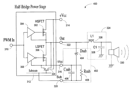
devices formed in
an integrated circuit in a substrate of the semiconductor as power switches,
such as power
MOSFETS. The switching devices may include a first switching device and a
second
switching device that are cooperatively switchable in a half bridge power
stage configuration
1
CA 02762135 2011-12-14
to generate an amplified output signal on an output node of the semiconductor.
The
semiconductor may also include a power supply input node for receiving a power
supply
voltage and a substrate node coupled with the substrate.
[0005] A resistor and a capacitor may be coupled in parallel between the power
supply input
node and the substrate node. The capacitor may be charged to a de-biasing
voltage during a
switching cycle of the first and second switching devices to reverse bias any
parasitic
switching devices that appear. The capacitor may be charged with a free-
wheeling current
that occurs during a time of a switching cycle of the first and second
switches (a free-
wheeling portion) when both the first and the second switching devices are not
substantially
conducting.
[0006] In one example configuration, the amplifier system may additionally
include a diode
coupled between the output node and the substrate node. The diode may be
forward biased
by the free-wheeling current to charge the capacitor. The diode may operate in
conjunction
with the resistor and capacitor as a shunt in parallel with a free-wheeling
body diode included
in one of the first switching device and the second switching device. A
forward voltage of
the diode may be less than a forward voltage of the free-wheeling body diode
included in one
of the first switching device and the second switching device so that the
diode turns on and
begins charging the capacitor before the free-wheeling body diode is turned
on.
[0007] An interesting feature of the amplifier system is that the resistor,
capacitor and diode
(if present) may be external to the semiconductor in some example
configurations.
Accordingly, the output node, the power supply input node and the substrate
node may each
be brought out of the semiconductor to a respective external pin of the
semiconductor.
[0008] Another interesting feature of the amplifier system is that any number
of switching
devices may be included. Accordingly, the amplifier system may include any
number of half
bridge power stages, or full bridge power stages. The resistor and capacitor
may be a
common charge/discharge circuit for each of the half bridge power stages or
full bridge
power stages.
[0009] Yet another interesting feature of the amplifier system is that the
system can provide
an inexpensive extension of a region of safe operation of the switching
devices by keeping
the parasitic switching devices substantially turned off. Extension of the
region of safe
operation of the switching devices can increase power output of the
semiconductor. When
the parasitic switching devices are kept off, not only are the regions of safe
operation of the
2
CA 02762135 2011-12-14
switching devices extended in terms of higher voltage and current, but also
noise currents and
electromagnetic interference (EMI) may be reduced. Noise current may result
from extended
free-wheeling body diode recovery times, and noise currents may result from
dynamic
avalanche at high voltages.
[0010] Other systems, methods, features and advantages of the invention will
be, or will
become, apparent to one with skill in the art upon examination of the
following figures and
detailed description. It is intended that all such additional systems,
methods, features and
advantages be included within this description, be within the scope of the
invention, and be
protected by the following claims.
BRIEF DESCRIPTION OF THE DRAWINGS
[0011] The invention may be better understood with reference to the following
drawings and
description. The components in the figures are not necessarily to scale,
emphasis instead
being placed upon illustrating the principles of the invention. Moreover, in
the figures, like
referenced numerals designate corresponding parts throughout the different
views.
[0012] Figure 1 is an example semiconductor architecture in the form of a CMOS
integrated
circuit architecture.
[0013] Figure 2 is the example semiconductor architecture of FIG. 1 with
examples of
parasitic switching devices illustrated.
[0014] Figure 3 is a circuit schematic of an example amplifier system that
includes a half-
bridge power stage.
[0015] Figure 4 is circuit schematic of the amplifier system of FIG. 3 that
includes a shunt
circuit.
[00161 Figure 5 is a circuit schematic of an example amplifier system that
includes a full-
bridge power stage and a shunt circuit.
[0017] Figure 6 is an operation flow diagram of an amplifier system.
DETAILED DESCRIPTION OF THE PREFERRED EMBODIMENTS
[0018] FIG. 1 is an example architecture for an integrated circuit (IC) 100
incorporated in a
semiconductor 102, such as a complimentary metal oxide semiconductor (CMOS)
power IC.
The example power IC is built upon a lightly doped P-type substrate using more
highly doped
3
CA 02762135 2011-12-14
N-wells to confine switching devices, such as P-channel MOSFETs, built upon
the same
substrate. In other examples, the switching devices may be other devices, such
as PNP
bipolar junction transistors (BJT), an insulated gate bipolar transistor
(IGBT), a thyristor, or
any other form of power transistor, mechanism or device included in an
integrated circuit and
capable of transitioning between a conducting and a non-conducting state.
Although the term
"MOSFETS" is used in the following discussion, it should be understood that
the switching
devices are not limited to MOSFET switching devices. The N-wells could be
biased, such as
by a power supply, to be more positively biased than any circuitry contained
within the IC
100. In other examples, the semiconductor may include P-wells in a lightly
doped n-type
substrate. In FIG. 1, NMOS devices may be built either directly on the
substrate or within N
tubs formed with deep N buried layers (NBL) supplied a positive supply voltage
(Vdd) by a
power supply. A negative supply voltage (Vss) supplied from a power supply may
be applied
to P-wells in the substrate.
[0019] The NMOS and PMOS devices may be formed in the substrate with a lateral
structure
in which the source (S), gate (G) and drain (D) are horizontally aligned.
Alternatively, or in
addition, NMOS and PMOS devices may be formed in the substrate with a vertical
structure.
The N-wells within P-epitaxial regions (P-epi) could also be used to contain
resistors, small
inductors and capacitors in addition to switching devices, such as MOSFETs.
Isolation using
silicon on insulator (SOI) approaches rather than a p-type substrate with N-
layer isolation
may also be used.
[0020] The monolithic nature of the construction creates parasitic devices.
Some examples
of parasitic bipolar devices 202 are indicated in FIG. 2. Switching devices,
such as
MOSFETs, can inherently contain a parasitic switching device, such as a
parasitic bi-polar
junction transistor (BJT) that can be local to each switching device. Although
the term "BJT"
is used in the following discussion, it should be understood that the
parasitic switching
devices should not be limited to a BJT, and may be any form of parasitic
switching device.
Not all of the parasitic NPN BJTs are shown in FIG. 2 that may appear in an
actual IC,
however, those shown in FIG. 2 can represent significant limitations to robust
functioning of
the IC. It is typical that the high current breakdown voltages of parasitic
switching devices
are considerably lower than the breakdown voltages of the switching devices of
which they
are a part. For example, at low BJT collector currents the breakdown voltages
are the equal
of the MOSFET drain to source breakdown voltages (BV dss) but not at high BJT
collector
4
CA 02762135 2011-12-14
currents. Therefore parasitic switching device currents, such as BJT collector
currents,
should be prevented from becoming large.
[0021] Conduction by such a parasitic switching device can be minimized by
design. In one
example, when the substrate of the semiconductor is joined/shorted to the
source of a
MOSFET, currents injected into the substrate tend to be returned to the source
rather than
allowed to enable the parasitic BJT. There can be three major sources of
charge to the base
of the parasitic transistors.
1. Displacement/capacitive current from a rapidly increasing drain-to-source
voltage
(V&)-
2. Charge left in the region by previous forward biasing of the drain to
substrate
junction.
3. Hot-carrier current (minority carriers) resulting from high electric fields
in the region
of the drain.
Capacitance between the drain and the substrate provides a significant turn-on
current for the
parasitic BJT that can be at least partially contained by a MOSFET design that
effectively
routes the current to the source lead of the MOSFET. This turn-on current,
however, is not
the only current that acts to enable a parasitic BJT.
[0022] Power converters, such as audio amplifiers may use power ICs to drive a
load. In
some examples, power converters using power ICs can drive into inductive
loads, such as
loudspeakers, using width modulation of high-frequency pulsed signals to
provide nearly-
lossless controlled delivery of energy to the inductive load. A class-D audio
amplifier is an
example of one such power converter.
[0023] FIG. 3 is an example amplifier system 300 having a half bridge power
stage that may
be included in a power converter. The half-bridge power stage may be
implemented with a
first switching device 302 driven by a first gate driver 304, and a second
switching device
306 driven by a second gate driver 308. The first and second gate drivers 304
and 308 may
drive the respective first and second switching devices 302 and 306 based on
an input signal
provided to an input node 310. The input node 310 may be an external pin on
the
semiconductor, or may be a part of the integrated circuit, which receives the
input signal.
[0024] The input signal may be one or more control signals, such as pulse
width modulated
signal. In an example of an audio amplifier system, the input signal may be a
pulse width
modulating signal generated by comparing a triangle wave to an audio signal
using a high
5
CA 02762135 2011-12-14
speed comparator to generate a series of pulses of varying width depending on
the
instantaneous amplitude of the audio signal. Alternatively, in another audio
amplifier system
example, a digital signal processor may generate the pulse width modulating
signal based on
an audio signal. The power converter may include other devices and systems,
such as
processors, memory, filters, a user interface, a communication interface, or
any other
functionality included in power converters, such as an audio amplifier.
[0025] The first and second switching devices 302 and 306 may be power MOSFETS
included as part of an integrated circuit in a substrate 312 of a
semiconductor. In a half-
bridge configuration, the first and second switching devices 302 and 306 may
be referred to
as a high side switch (HSFET), and a low side switch (LSFET), respectively.
[0026] The integrated circuit may be supplied power from one or more external
power
supplies. In FIG. 3, a first power supply input node 314 may receive a
positive power supply
voltage (+Vcc) as an input voltage. The first power supply input node 314 may
include an
external pin on the semiconductor that is also coupled internal to the IC
through the substrate
312 with the first switching device 302. A second power supply input node 316
may receive
a negative power supply voltage (-Vcc) as an input voltage. The second
switching device
306 and the second gate drive 308 may be coupled through the substrate 312
with the second
power supply input node 316 internal to the IC. The second power supply input
node 316
may also include an external pin on the semiconductor.
[0027] The voltage received at the second power supply input node 316 may be a
most
negative power supply (-Vcc) of the amplifier half-bridge. Accordingly, the
voltage received
at the second power supply input node 316 may be the most negative supply
voltage potential
of the second switching device 306. In some examples, the most negative power
supply (-
Vcc) may be ground. In other power IC examples, the most negative power supply
(-Vcc)
may be greater than or less than zero volts. In still other examples, the
power supply inputs
may be reversed such that the first power supply input node 314 receives the
negative power
supply voltage (-Vcc), and the second power supply input node 316 receives the
positive
power supply voltage (+Vcc) based on whether the switching devices are N type
or P type
devices, such as NMOS and PMOS devices. Thus, in the following discussion,
although not
indicated, the positive and negative supply voltages may be interchanged.
[0028] In FIG. 3, the substrate 312 is coupled with the negative power supply
(-Vcc) by a
jumper circuit 318. The jumper circuit 318 forms a short circuit between the
second power
6
CA 02762135 2011-12-14
supply input node 316 and a substrate input node 320. The substrate input node
320 is in the
form of an external pin that is external to the semiconductor. Accordingly,
the shunt circuit
318 is external to the semiconductor. In other examples, the substrate 312 may
be coupled to
the negative power supply (-Vcc) by a shunt circuit 318 that is internal to
the semiconductor
and included within the IC.
[0029] During operation, the half-bridge power stage 300 generates an output
signal on an
output node 322, which may be provided as an external pin on the
semiconductor. The
output signal may represent the amplified input signal provided on the input
node 310. The
output node 322 may be coupled to one or more filters 324, such as a passive
filter containing
one or more inductors (L 1) 326, and one or more capacitors (C l) 328. In
other examples, an
active filter, or any other type of filter may augment the filter 324. The
filter 324 may also be
included as part of the integrated circuit included in the semiconductor in
other example
configurations. Accordingly, in some examples, the output signal generated by
the half-
bridge power stage 300 may not be directly supplied to an external pin on the
semiconductor.
The output node 322 may also be coupled with a load 330. The load 300 may be
any device
capable of receiving the output signal. In FIG. 3, the load 330 includes one
or more
loudspeakers, which are driven by the output signal to produce audible sound.
[0030] During operation of the amplifier system 300 one or more parasitic
switching devices
334, such as a parasitic BJT may appear in the integrated circuit (IC)
contained in the
semiconductor. In one example, the parasitic switching device(s) 334 may be
parasitic NPN
BJTs. During operation charge may be driven into the parasitic switching
device 334 by
current that flows when the first switching device 302 (high-side FET - HSFET)
turns off and
a portion of the current in the inductor 326 (L I) is forced to flow into the
output node 322
and through the forward biased body diode or substrate diode of the second
switch 306 (low-
side FET - LSFET). The body diode or free-wheeling body diode may be included
in each of
the first and second switching devices 302 and 306 between a drain and a
source of the
respective switching device.
[0031] This portion of the conversion cycle when switching off either the
first or the second
switching device 302 or 306 and before switching on the alternate switching
device (either
the first or the second switching device 302 or 306) may be described as a
free-wheeling
portion of the cycle. In the case of the first switching device (HSFET) 302
being switched
off, the free-wheeling portion of the cycle, without subsequent switching,
would last until the
7
CA 02762135 2011-12-14
current in the inductor 326 (Li) reverses direction due to the second
switching device 306
(LSFET) conducting and supplying voltage and current on the output node 322.
For
example, the second switching device 306 may begin conducting in the direction
where the
FET channel is conducting using only majority carriers. At relatively high
instantaneous
output currents, the alternate switching device (FET) may turn on before the
current reverses
direction in the inductor 326 (L1).
[0032] The full turn-on of the parasitic switching device 334 can occur when
the first
switching device 302 (HSFET) is suddenly turned on with the free-wheeling
current still
flowing into the free-wheeling body diode of the second switching device 306
(LSFET).
This may be referred to as a parasitic switching device charging event. In
some cases, the
parasitic switching device 334 may be biased on during the free-wheeling cycle
but may lack
sufficient collector potential to conduct enough current to pose a problem
until the first
switching device 302 (HSFET) turns on and forces voltage across the parasitic
switch device
334, such as across a collector circuit of a parasitic BJT to detrimentally
increase the current
conducted.
[0033] In some examples, a portion of the parasitic switching device 334, such
as a parasitic
BJT's collector, may terminate on a guard ring. The guard ring may be a
construct of the
integrated circuit, and may be used to collect spurious current in order to
minimize spurious
cross talk in the IC. The guard ring may be biased with a positive (or
negative) potential with
respect to the substrate 312, such as being biased with at least a portion of
the positive power
supply (+Vcc). As such, the voltage across the parasitic switching device 334
may be even
larger when free-wheeling current is still flowing into the body diode of the
second switching
device 306 (LSFET) and the first switching device 302 (HSFET) is suddenly
turned on.
[0034] During operation, when the first switching device 302 (HSFET) begins to
turn on hot-
carriers may be generated near the drain of the first switching device 302
(HSFET). When
the drain-source voltage of the first switching device 302 (HSFET) is
sufficiently large, there
is sufficient energy in the majority carriers (electrons) to dislodge
electrons from the silicon
lattice of the first switching device 302 (HSFET). The freed electrons join
the flow towards
the drain of the first switching device 302 (HSFET). Some of the resulting
holes may flow
into the substrate 312 and energize the parasitic switching device 334. The
hole current may
be proportional to the drain current and exponentially related to the drain-
source voltage.
8
CA 02762135 2011-12-14
The expression for hot-carrier current in the first switching device 302
(HSFET) may be
provided in the form:
Em
Impact = J Id = A = e-B/E(x) = dx Equation 1
Es
Where ES is the field at the source, Em is the maximum field and E(x) is the
local field along
the integration path in x. Id is the drain current and A and B are
semiconductor material
related coefficients.
[0035] Since the voltage is high with high drain current (Id) only during the
time that the first
switching device 302 (HSFET) is recovering the body diode of the second
switching device
306 (LSFET) and slewing the output node 322, the time dimensions of the hot-
carrier event,
or parasitic switching device charging event, may be limited. Unfortunately,
the heightened
recovery tail of the body-diode of the second switching device 306 (LSFET)
(due to the turn
on of the first switching device 302 (HSFET)) may increase the drain current
(Id) well above
the current needed to support the current in the inductor (LI) 326. If one
attempts to
minimize the time integral of the impact current (Iimpact), which corresponds
to a charge, such
as a BJT base charge, of the parasitic switching device 334, by turning on
first switching
device 302 (HSFET) faster, then a magnitude of the drain current (Id) may be
increased. An
increase in the drain current (Id) of the first switching device 302 (HSFET)
may offset many
of the gains made by reducing the width of the hot-carrier pulse. In other
words, an increased
drain current (Id) reduces integration of charge during the shorter time of
the hot carrier event
(parasitic switching device charging event), however peak currents increase,
so an amplitude
of hot carriers increases resulting in additional charging and activation of
the parasitic
switching device 334.
[0036] Therefore anything allowing a reduction in the drain current Id of the
first switching
device 302 (HSFET) may reduce Iimpact. While it may not be possible to
eliminate 'impact, it
may be possible to keep the drain current (Id) from activating the parasitic
switching device
334, or minimize activation, during a parasitic switching device charging
event. It may also
be possible to use some of the large free-wheeling current that otherwise
would have charged
the parasitic switching device 334, such as charging the base region of a
parasitic BJT, to
9
CA 02762135 2011-12-14
deliver a charge to a temporary reservoir that can act to de-bias the
parasitic switching device
334. In other words, a portion of the drain current (Id) of the first
switching device 302
(HSFET) may be shunted or diverted to an alternative current flow path during
the parasitic
switching device charging event to avoid charging the parasitic switching
device 334 to the
s point of turn on, or full turn on.
[0037] FIG. 4 is another example amplifier system 400 having a half bridge
power stage that
may be included in a power converter. The half bridge power stage may include
the first
switching device 302 and the first gate driver 304, and the second switching
device 306 and
the second gate driver 308, formed in the substrate 312. The input node 310
may received an
input signal, such as a pulse-width modulated signal, and the output node 322
may provide an
amplified output signal formed by amplification of the input signal using the
first and second
switching devices 302 and 306. The output signal may be provided to one or
more filters 324
and supplies one or more loads 330. Accordingly, the amplifier system 400 is
similar in
many respects to the previously discussed amplifier system 300 described with
reference to
FIG. 3. For purposes of brevity, the previous discussion will not be repeated,
but may be
wholly or partially applicable.
[0038] In FIG. 4, the amplifier system 400 includes a shunt circuit 402 that
acts to de-bias the
parasitic switching device 334, such as a parasitic BJT, by using the free-
wheeling cycle of
the half-bridge power stage to advantage. The shunt circuit 402 may include a
diode (Dsub)
404, a capacitor (Csub) 406, and a resistor (Rsub) 408. The shunt circuit 402
may be parallel
to the free-wheeling body diode of the second switching device 306.
[0039] The diode (Dsub) 404 may be coupled between the output node 322, and
the substrate
node 320. The diode (Drub) 404 may be any diode capable of having a reverse
blocking
voltage rating of at least a difference in voltage magnitude between the
positive power supply
voltage (+Vcc) and the negative power supply voltage (-Vcc) received at the
first power
supply input 314, and a forward voltage (Vf) which is less than the forward
voltage (Vt) of
the body diode or substrate diode of the second switching device 306 (LSFET).
In one
example, the diode (Dsub) may be a Schottky diode.
[0040] The diode (Dsub) 404 may be external to the semiconductor and therefore
may not be
formed in the substrate 312. Alternatively, the diode (Dsub) 404 may be formed
as part of
the integrated circuit included in the semiconductor. The diode (Dsub) 404 may
receive only
a relatively small predetermined portion of the total current that is possible
on the output
CA 02762135 2011-12-14
node 322. Accordingly, the current rating of the diode (Dsub) 404 may be
substantially less
than the total expected output current of the output signal on output node
322. In one
example, the diode (Dsub) 404 may be rated at about twenty percent of the
highest expected
output current of the output signal on the output node 322. Accordingly, diode
(Dsub) 404
may be a practical part to deploy both from a size and cost standpoint.
[0041] The difference voltage between the forward voltages of the body diode
or substrate
diode of the second switching device 306 (LSFET) and the diode (Dsub) 404 may
be the
measure to which the capacitor (Csub) 406 can be charged to reverse bias the
parasitic
switching device 334, such as to reverse bias a BJT base-emitter junction.
Accordingly, the
capacitor (Csub) 406 may act as a temporary reservoir for some of the large
free-wheeling
current that otherwise would charge the parasitic switching device 334, such
as charging the
base region of a parasitic BJT, during a parasitic switching device charging
event. Delivering
the charge to the temporary reservoir can act to de-bias the parasitic
switching device 334, as
previously discussed.
[0042] The capacitor (Club) 406 may be charged to a voltage that is just below
the negative
power supply voltage (-Vcc) received as an input voltage on the second power
supply input
316. The voltage stored in the capacitor (Csub) 406 may be enough to lower the
voltage
potential of the substrate 312 a predetermined amount below the negative power
supply
voltage (-Vcc). The predetermined amount of de-biasing voltage below the
negative power
supply voltage (-Vcc) may be enough to avoid biasing the parasitic switching
device 334 on
during a parasitic switching device charging event, without causing shifts in
operational
characteristics of other devices in the integrated circuit formed in the
substrate 312. For
example, substantial body-induced threshold shifts in the first and second
switching devices
302 and 304 (FETs) that are built in the substrate 312 may be avoided if the
de-biasing
voltage remains relatively small. Thus, the shift in voltage potential of the
substrate 312 may
be less than the gate threshold voltage of any device that is built directly
on the substrate 312
to reduce the risk of unintended crosstalk through the substrate 312. In one
example, the de-
biasing voltage stored as a charge on the capacitor (Csub) 406 may be in a
range of hundreds
of millivolts below the negative power supply voltage (-Vcc). Thus, the
voltage potential of
the substrate 312 may be shifted in a range of hundreds of millivolts.
[0043] The resistor (Rsub) 408 may be coupled in parallel with the capacitor
(Csub) 406 and
cooperatively operates with the capacitor (Csub) 406 as a charge/discharge
circuit. This
11
CA 02762135 2011-12-14
charge/discharge circuit may be coupled between the second power supply input
316 and the
substrate node 320. The resistor (Rsub) 408 may have a resistance value that
provides for
diversion of any leakage currents flowing within the power stage or reverse
bias leakage of
the diode (Dsub) 404 in the absence of any forward conduction in the diode
Dsub 404.
Accordingly, the resistor (Rsub) may be a relatively small resistance, such as
in a range of
about 1 Ohms to about 100 Ohms.
[0044] The capacitor (Csub) 406 may have low equivalent series inductance
(ESL) and
equivalent series resistance (ESR) with a capacitance which is large compared
to a zero bias
capacitance of the parasitic switching device 334. In one example, the
capacitor (Csub) 406
may be in a range of about 10's of nanoFarads. The capacitance value of the
capacitor (Csub)
406 may be increased with the size and number of second switching devices 306
(LSFETs)
included in the power stage(s). The capacitor (Csub) 406 may be physically
located or placed
external to but very near the IC. The internal impedances of bond wires and
metalizations in
the IC interconnecting the capacitor (Csub) 406 via the second power supply
input 316 and
the substrate node 320 should be minimized. The physical placement of the
resistor (Rsub)
408 and the diode (Dsub) 404 with respect to the IC and the capacitor (Csub)
406 are less
sensitive. Alternatively, in other example configurations of the amplifier
system, either one
or both of the capacitor (Csub) 406 and the resistor (Rsub) 408 may be formed
in the
substrate as part of the IC.
[0045] In another example, the diode (Dsub) 404 may be omitted from the shunt
circuit 402
such that only the resistor (Rsub) 408 and the capacitor (Club) 406 of the
charge/discharge
circuit are in parallel with the free-wheeling body diode of the second
switching device 306.
In the absence of the diode (Dsub) 404, the shunt circuit 402 may be designed
to rely on the
added substrate impedance provided by resistor (Rsub) 408 to allow pumping
(charge and
discharge) of the capacitor (Csub) 406 using the body diode to substrate
conductivity of the
second switching device (LSFET) 306. Accordingly, the capacitor (Csub) 406 may
be
charged to the de-biasing voltage in order to adjust the voltage potential of
the substrate 312
an amount to reverse bias the parasitic switching device 334, as previously
discussed.
[0046] FIG. 5 is another example amplifier system 500 included in a power
converter. In this
example, the amplifier system 500 includes a full-bridge power stage that is
built on a
common substrate 502. In FIG. 5, a first switching device 504 is operable with
a first gate
driver 506, and a second switching device 508 is operable with a second gate
driver 510 to
12
CA 02762135 2011-12-14
form a first half-bridge power stage. The first and second gate drivers 506
and 510 are driven
with an input signal, such as a pulse-width modulated signal, on a first input
node 514. In
addition, a third switching device 518 is operable with a third gate driver
520, and a fourth
switching device 522 is operable with a fourth gate driver 524 to form a
second half-bridge
power stage. The third and fourth gate drivers 520 and 524 are driven with a
second input
signal, such as a pulse-width modulated signal, on a second input node 528.
The first and
second input signals may be separate signals, or the first input signal may be
inverted to form
the second input signal.
[0047] The first and second switching devices 504 and 508 may cooperatively
operate to
generate a first output on a first output node 532, and the third and fourth
switching devices
518 and 522 may cooperatively operate to generate a second output on a second
output node
534. The first and second outputs may be positive and negative amplified
output signals,
which are filtered by respective filters 536 and used to drive a load 538.
Power supplied by a
positive power supply voltage (+Vcc) on a first power supply input node 540
and a negative
power supply voltage (-Vcc) on a second power supply input node 542 may be
used to
generate the first and second output signals. In FIG. 5, during operation one
or more parasitic
switching devices 544, such as a parasitic BJT may appear in the integrated
circuit (IC)
contained in the semiconductor. In one example, the parasitic switching
device(s) 544 may
be parasitic NPN BJTs, and the switching devices may be N channel power
MOSFETS, as
previously discussed.
[0048] The features and alternatives of the previously discussed example
amplifier systems
are fully, or at least partially applicable to the audio amplifier system 500,
and for brevity
purposes are not repeated. In other examples, any number of full bridge power
stages, or half
bridge power stages may be included in an amplifier system of a power
converter.
[0049] A shunt circuit 548 may also be included in the amplifier system 500.
In FIG. 5, the
shunt circuit 548 may include a resistor (Rsub) 550, a capacitor (Csub) 560
coupled in
parallel and forming a charge/discharge circuit coupled between a substrate
node 562 and the
second power supply input node 542. The shunt circuit 548 may also include a
first diode
(Dsub+) 564 coupled between the positive amplified output signal on the first
output node
532 and the substrate node 562, and a second diode (Dsub-) 566 coupled between
the
negative amplified output signal on the second output node 534 and the
substrate node 562.
The first and second output nodes 532, 534, the first and second power supply
input nodes
13
CA 02762135 2011-12-14
540 and 542, and the substrate node 562 may be formed as external pins on the
semiconductor. Accordingly, the resistor (Rsub) 550, the capacitor (Csub) 560,
and the first
and second diodes 564 and 566 (if present) may be external to and coupled with
the
semiconductor, as previously discussed. Alternatively, any of the resistor
(Rsub) 550, the
capacitor (Csub) 560, and/or the first and second diodes 564 and 566 (if
present) may be
formed as part of the IC.
[0050] The resistor (Rsub) 550 and the capacitor (Csub) 560 may be a shared
common
charge/discharge circuit used with each of the first and second diodes 564 and
566.
Accordingly, other example amplifier systems containing additional channels,
can practice
the same methods by adding diodes from the additional output nodes and sharing
the
common charge/discharge circuit formed by the resistor (Rsub) 550 and the
capacitor (Csub)
560. Such multi-channel designs may practice phase staggering of the output
switching,
which poses no problems as each half bridge power stage provides the necessary
pump-down
(up) capacitive charging to adjust the voltage potential of the substrate) for
its respective
HSFET turn-on cycle and the small added substrate bias is not problematic to
the remaining
channels that do not need a pump-down at that particular instant in time.
Alternatively, in
other examples, multiple charge/discharge circuits may be included in the
amplifier system to
support the multiple channels.
[0051] Similar to the previously discussed examples, the capacitor (Club) 560
may be
charged to a voltage that is just below the negative power supply voltage (-
Vcc) (or the
positive voltage +Vcc with an n-type substrate) received as an input voltage
on the second
power supply input node 542. The voltage stored in the capacitor (Csub) 406
may be a de-
biasing voltage that adjusts the voltage potential of the substrate 502 to
reverse bias the
parasitic switching device(s) 544. For example, the de-biasing voltage may
lower the voltage
potential of the substrate 502 below the negative power supply voltage (-Vcc)
enough to
avoid biasing of the parasitic switching device(s) 544 during a parasitic
switching device
charging event occurring in any one of the half-bridge power stages.
[0052] In another example, the first and second diodes (Dsub) 564 and 566 may
be omitted
from the shunt circuit 548. In the absence of the first and second diodes
(Dsub) 564 and 566,
the shunt circuit 548 may be designed to rely on the added substrate impedance
provided by
resistor (Rsub) 550 to allow pumping of the capacitor (Csub) 560 using the
body diode to
substrate conductivity of the second switching devices (LSFETs) 508 and 522.
Accordingly,
14
CA 02762135 2011-12-14
the capacitor (Club) 560 may be charged to the de-biasing voltage in order to
adjust the
voltage potential of the substrate 502 a predetermined amount with respect to
the negative
power supply voltage (-Vcc) in order to reverse bias the parasitic switching
device 544.
Multi-channel power converters may similarly be designed to omit the diodes
(Dsub) from
the respective channels.
[0053] FIG. 6 is an operational flow diagram of an example amplifier system
described as
previously discussed with reference to FIGs. 1-5. The operation begins at
block 602, when
a first switching device (HSFET) is turned on, and voltage and current are
supplied as an
amplified output signal on an output node for supply to a load. The voltage in
the output
signal is applied to the inductor (L) in the filter, and energizes the
inductor (L) at block 604.
The first switching device (HSFET) is turned off at block 606, and a second
switching device
(LSFET) is not yet turned on within a half-bridge power stage of a power
converter. At block
608, the half-bridge power stage enters the free-wheeling portion of the power
conversion
cycle where the inductor (L) is de-energized and current is generated.
[0054] The forward voltage of the diode (Dsub) is reached or not reached at
the output node
at block 610 based on the current generated in the inductor (L) and the
voltage present at the
output node. If the forward voltage of the diode (Dsub) is not reached, the
diode Dsub
remains off and the operation returns to block 610. If the forward voltage of
the diode (Dsub)
is reached, the diode Dsub turns on and begins conducting current to the
substrate node at
block 612. The voltage potential of the substrate is adjusted at block 614 to
be below the
negative supply voltage (-Vcc) by charging the capacitor (Csub). At block 616,
the body
diode of the second switching device (LSFET) is turned on and begins to
conduct and free-
wheeling current flows into the body diode of the second switching device
(LSFET). The
parasitic switching device is reversed biased by the adjusted substrate
voltage and remains
turned off at block 618. Operation on an n-type substrate can be understood by
interchanging
the terms HSFET with LSFET, above with below and +Vcc with -Vcc in the
foregoing
description. In such circumstance the parasitic device can be, for example, a
PNP BJT.
[0055] The previously discussed examples of an amplifier system include an
integrated
circuit having a substrate with a plurality of cooperatively operating power
switching devices
formed in the substrate to provide amplification of an input signal. The
amplifier system may
also include a shunt circuit having a substrate charge/discharge circuit and
one or more
substrate diodes that may be located external to the IC. The substrate
diode(s) may be turned
CA 02762135 2011-12-14
on during a free-wheeling portion of a switching cycle of the power switching
devices to
charge the substrate capacitor and thereby adjust a voltage potential of the
substrate. The
voltage potential of the substrate may be adjusted to reverse bias one or more
parasitic
switching devices that appear in the IC during the free-wheeling portion of
the switching
s cycle. Accordingly, full turn on of the one or more parasitic switching
devices and the
subsequent possibility of failure in the integrated circuit may be minimized
or avoided.
[0056] While various embodiments of the invention have been described, it will
be apparent
to those of ordinary skill in the art that many more embodiments and
implementations are
possible within the scope of the invention. Accordingly, the invention is not
to be restricted
except in light of the attached claims and their equivalents.
16