Note: Descriptions are shown in the official language in which they were submitted.
CA 02762140 2011-11-15
WO 2010/132074
PCT/US2009/061866
METHOD AND APPARATUS FOR SIGNAL INVERSION
IN SUPERCONDUCTING LOGIC GATES
BACKGROUND
Field of the Invention
[0001] The disclosure relates to a method and apparatus for signal inversion
in superconducting
logic gates. More specifically, the disclosure relates to a method and
apparatus for configuring
signal inversion in quantum logic gates which process single flux quantum
(SFQ) pulses.
Description of Related Art
[0002] In the field of digital logic, extensive use is made of well known and
highly developed
CMOS (complementary metal-oxide semiconductor) technology. As CMOS has begun
to
approach maturity as a technology, there is an interest in alternatives that
may lead to higher
performance efficiency in terms of speed, power-computational density,
interconnect bandwidth
and the like.
[0003] An alternative approach to CMOS technology comprises superconductor-
based single
flux quantum circuitry, utilizing superconducting Josephson junctions, with
typical signal power
of around 4 nW, at a typical data processing rate of 20 Gb/s or greater. Such
devices have
operating temperatures of about 4 K.
[0004] Superconductor devices based on the Josephson effect are replacing
conventional
devices based on semiconductor technology for higher performance and lower
power. The
superconductor devices are well known as a high-speed, low-power digital logic
family and are
scalable to very-large scale integrated (VLSI) circuits. Digital circuits that
employ
superconductor devices and are fabricated using present circuit fabrication
technology operate at
clock rates ranging between 10-100 GHz. Development of advanced
superconducting devices
require sophisticated Josephson junction logic gates that operate based on the
superconducting
principles. Therefore, there is a need for such advanced logic gates.
-1-
CA 02762140 2011-11-15
WO 2010/132074
PCT/US2009/061866
SUMMARY
[0005] In one embodiment, the disclosure relates to a single-flux-quantum
logic gate capable of
providing output from one of the two inputs, which is also known as the A and
NOT B gate. The
logic gate includes a first and a second input gates for respectively
receiving a first and a second
input pulses. An output gate is wired in parallel with the first input gate. A
first Josephson
junction and a second Josephson junction are connected to the first input gate
and the second
input gate, respectively. A cross-coupled transformer is also provided. The
cross-coupled
transformer diverts the first pulse from the output gate if the second pulse
is detected at the
second input gate.
[0006] In an exemplary method according to one embodiment of the disclosure, a
method for
providing a quantum logic gate includes the steps of providing a quantum logic
circuit to have a
first and a second input gate as well as an output gate; receiving a first
input pulse at the first
gate; directing the quantum logic gate to propagate the first input pulse to
the output gate if a
second input is not received at the second input gate; and directing the
quantum logic gate to
inhibit propagation of the first input pulse to the output gate if a second
input pulse is received at
the second input gate.
[0007] In another embodiment, the disclosure relates to a single-flux-quantum
logic gate
circuit. The logic gate comprises a first input gate connected in parallel to
the first Josephson
junction and a second input gate connected in parallel to the second Josephson
junction. An
output gate is configured to be in communication with the first and the second
input gates. A
circuit defining an offset coupling is also provided to inhibit certain flux
propagations while
encouraging certain other propagations. Finally, a cross-coupled transformer
connecting the first
Josephson junction and the second Josephson junction is provided.
[0008] In still another embodiment, the disclosure relates to a merge gate for
use in single-flux-
quantum circuits. The single-flux-quantum merge gate circuit includes a first
input gate and a
second input gate for respectively receiving the first input pulse and a
second input pulse. The
first and the second input gates are coupled respectively to a first Josephson
junction and a
second Josephson junction. A pair of cross-coupled transformers connect the
first Josephson
10055731.1
-2-
CA 02762140 2011-11-15
WO 2010/132074
PCT/US2009/061866
junction to the second Josephson junction such that a first input received at
the first input gate is
prevented from propagating to the second input gate and is instead directed to
an output gate.
[0009] In still another embodiment, the single-flux-quantum logic gate circuit
includes a first
input gate and a second input gate for respectively receiving a first input
pulse and a second
input pulse, the first input gate coupled to a first Josephson junction and
the second input gate
coupled to a second Josephson junction; a pair of cross-coupled transformers
connecting the first
Josephson junction to the second Josephson junction; a first output gate and a
second output gate
in communication with the pair of cross-coupled transformers; and an offset
coupling for biasing
the transformer to direct one of the first input pulse or the second input
pulse to the first output
gate when only one input is received during one clock cycle.
100101 In another embodiment, the disclosure relates to a method for
controlling an output of a
logic gate by (i) receiving a first reciprocal SFQ pulse at a first input gate
and triggering a first
Josephson junction in communication with the first Josephson junction; (ii)
receiving a second
reciprocal SFQ pulse at a second input gate and triggering a second Josephson
junction in
communication with the second Josephson junction; (iii) providing a first bias
current to direct
one of the first reciprocal SFQ pulse or the second reciprocal SFQ pulse to a
first output if only
one of the first reciprocal SFQ pulse or the second reciprocal SFQ pulse is
received during one
clock cycle; and (iv) directing the second reciprocal SFQ pulse to a second
output if the first and
the second input signals are received during one clock cycle.
10055731.1
-3-
CA 02762140 2011-11-15
WO 2010/132074
PCT/US2009/061866
BRIEF DESCRIPTION OF THE DRAWINGS
[0011] These and other embodiments of the disclosure will be discussed with
reference to the
following exemplary and non-limiting illustrations, in which like elements are
numbered
similarly, and where:
[0012] Fig. lA shows a conventional reciprocal quantum logic Josephson
Transmission Line
("JTL");
[0013] Fig. 1B shows the signal response of the JTL of Fig. 1A;
[0014] Fig. 1C shows a conventional offset coupling;
[0015] Fig. 2A schematically shows a logic gate according to one embodiment of
the
disclosure;
[0016] Fig. 2B is a circuit diagram for the logic gate of Fig. 2A;
[0017] Fig. 3A is a schematic representation of a merge gate according to one
embodiment of
the disclosure; and
[0018] Fig. 3B is a circuit diagram for the logic gate of Fig. 3A;
[0019] Fig. 4A is a schematic representation of an AND/OR gate according to
one embodiment
of the disclosure;
[0020] Fig. 4B shows the current flow in logic gate of Fig. 4A before any
input is received;
[0021] Fig. 4C shows the current flow in logic gate of Fig. 4A after first
input pulse but before
any output;
[0022] Fig. 4D shows the current flow in logic gate of Fig. 4A after the first
input and after an
OR output;
[0023] Fig. 4E shows the current flow in logic gate of Fig. 4A after first and
second inputs are
received and after OR output is provided; and
[0024] Fig. 4F shows the current flow in logic gate of Fig. 4A after first and
second inputs and
after outputs at both output gates.
10055731.1
-4-
CA 02762140 2011-11-15
WO 2010/132074
PCT/US2009/061866
DETAILED DESCRIPTION
[0025] Fig. lA shows a conventional reciprocal quantum logic circuit. More
specifically, the
logic circuit 100 of Fig. 1A is a Josephson Transmission Line ("JTL") having
Josephson junction
104. Input pulse A is provided to Josephson junction 104 through inductor 102.
Inductor 102
may be optionally added to filter out the harmonics associated with the input
signal. AC power
source is provided to a transformer 105 which comprises primary loop 106 and
secondary loop
108. Output of JTL 105 is provided at gate Q.
[0026] Fig. 1B shows the signal response of the JTL of Fig. 1A. Referring
simultaneously to
Figs. lA and 1B, when AC power is provided to transformer 105, the circuit is
powered as
shown by the trapezoidal flux Ls across inductor 108. If pulse input signal A
is provided while
inductor 108 is at a positive flux 109, the voltage pulse appears across
Josephson junction 104 as
noted by b1 in Fig. 1B. Pulse train b1 contains both positive and negative
pulses. The negative
pulse reflects resetting of the Josephson junction while inductor 108 is at
negative flux.
[0027] Fig. 1 C shows a conventional offset coupling. Referring to Fig. 1C,
nodes 160 and 162
are floating terminals which can be connected to a JTL or other circuits.
Inductors 152 and 158
form mutual inductance (Lm) when DC current 154 is supplied. The offset
coupling of Fig. 1C
can be used to establish bias current in an inductive loop. A flux bias of one-
half of a single-flux-
quantum, provided by the circuit of Fig. 1C can be calculated according to the
following
relationship:
LmIde = 1/2 (Do (1)
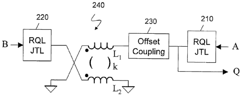
[0028] Fig. 2A schematically shows a logic gate according to one embodiment of
the
disclosure. More specifically, the circuit schematically represented in Fig.
2A provides a so-
called A-and-NOT-B logic gate. The A-and-NOT-B gate operates by receiving
inputs at a first
gate and a second gate. If an input is received at the first gate while no
input is received within
the same clock cycle at the second gate, the received input is directed to the
output. On the other
hand, if a second input is received at the second input gate within the same
clock cycle as
receiving a first input at the first input gate, then the logic gate provides
no output. In general, the
second input must lead or be approximately coincident in time with the first
pulse.
10055731.1
-5-
CA 02762140 2014-11-19
The circuit of Fig. 2A comprises a first input gate for receiving the first
input A, and a second
input gate for receiving the second input B. Each of inputs A and B can define
an SFQ pulse of
magnitude CDo. Moreover, inputs A and B may be received during the same clock
cycle. In Fig.
2A, each input gate may be incorporated into an RQL JTL similar to those
described in relation
to Fig. 1A. Thus, input A may be received at RQL JTL 210 and input B may be
received at RQL
JTL 220. Offset coupling 230 can comprise a conventional offset coupling as
described in Fig.
IC.
[0029] Finally, cross-coupled transformer 240 includes a first and a second
inductor providing
inductance L1 and L2, respectively, and having a coupling constant, k. Cross-
coupled
transformer 240 inverts signal B arriving from the second input gate. The loop
inductance (Lkop)
of transformer 240 can be described according to the following relationship:
L.1001, --- LI + L2 - 2k. LA (2)
[0030] In Equation 2, the term 2k. ,./L,L, denotes the mutual inductance
between the inductors.
The coupling constant can be assumed to he near unity (at about 0.9), and Li
and L2 can be
assumed to be approximately equivalent. Therefore, the loop inductance LI." is
much smaller
than either inductance L1 or L2 taken individually. The flux bias current set
up by the offset
coupling can be described according to:
1/2 ((Do /Ltoop) (3)
In Equation 3, the current I is approximately equal in magnitude in the
inductors Li and L2 but
flows in opposite direction in these two inductors.
[0031] When a first input pulse A is provided to RQL .ITL210, the input pulse
is directed to
output Q if a second input pulse B is not received at RQL JTL 220 during the
same clock cycle as A. Offset
coupling 230 negates propagation of pulse A to input gate B. In an exemplary
embodiment,
offset-coupling 230 enhances the AC power that causes the junction at RQL JTL
210 to trigger.
[00321 As discussed in relation to Equation 1, the offset coupling can be in
the order of1/2 (Do,
where (Do defines flux output of signal A. The flux output of offset coupling
may flow in an
opposite direction from that of input A and the flux output will have a
negative sign associated
therewith (1/2 (1) 0). In one embodiment, (Do has a magnitude of about 2mApH.
10055731
-6-
CA 02762140 2014-11-19
[0033] If input pulse B is provided during the same clock cycle as input pulse
A, the input
pulse B is directed to cross-coupled transformer 240 which inverts signal B
and inhibits
propagation of any output through Q.
[0034] In an alternative embodiment of the disclosure, offset coupling 230 is
removed from the
circuit. Instead, the Josephson junctions and bias inductors used in RQL JTL
210 and 220 are
selected so as to allow propagation of A to output Q when there is no input B.
[0035] Fig. 2B is a circuit diagram for the logic gate of Fig. 2A. Circuit 250
of Fig. 2A is flux-
biased through a DC current source and a transformer having inductors 254 and
256. Inductors
254 and 256 power circuit 250 through mutual inductance Lm. A combination of
DC current
source (Ide) and inductors 254 and 256 define offset coupling 230 of Fig. 2A.
[0036] Input gates A and B respectively receive input pulses A and B. Input
filters 252 and
262 may be optionally added to input gates A and B, respectively. Inductors
258 and 260 are
wired between the first Josephson junction (El) and the second Josephson
junction (JJ2) and
define the cross-coupled transformer 240 of Fig. 2A.
[0037] When circuit 250 receives input pulse A, the pulse travels through
inductor 252. If
during the same clock cycle no input is received at the second input gate,
then pulse A is directed
to output Q, which path is enhanced by the flux output (-1/2 00) of the offset
coupling 251. The
output of the offset coupling 251 encourages pulse A to trigger J.Ji and
propagate to output Q.
The triggering of DI reverses the flux output of the offset coupling 251 to
(+1/2 '1)o) This reverses
the current flow through JJ2 and inhibits triggering of JJ2 and propagation of
the signal to input
B.
[0038] On the other hand, when circuit 250 receives input pulse A and input
pulse B during the
same clock cycle, the input B triggers JJ2, which reverses the flux output of
the offset coupling
251 to (+1/2 (Do) This reverses the current flow through HI and inhibits A
from propagating to
output Q. Under this circumstance, Josephson junctions JJ2 is triggered and
admits a pulse (00)
into the circuit. No output pulse is provided at Q. The inputs to circuit 250
are reciprocal; that
is, each positive input pulse is followed by a negative input pulse which
effectively resets the
Josephson junctions. In other words, the residual signals stored in the gate
during the positive
cycle are removed in the negative cycle of the input pulse.
10055731]
-7-
CA 02762140 2011-11-15
WO 2010/132074
PCT/US2009/061866
[0039] Fig. 3A is a schematic representation of a merge gate according to one
embodiment of
the disclosure. The merge gate of Fig. 3A can be constructed using the circuit
segments
discussed above. In Fig. 3, the pulse inversion property of the loop
transformer steers the input
pulse to the output and prevents it from propagating to the opposite input
gate.
[0040] Circuit 300 of Fig. 3A includes input gates 301 and 302 for
respectively receiving input
pulses A and B, respectively. JTL 310 communicates with input gate 301 and JTL
320
communicates with input gate 302. Either of JTL 310 or 320 can define RQL JTL,
such as those
discussed above. Circuit 340 includes a pair of cross-coupled transformers
connecting JTL 310
and 320 such that input A received at input gate 301 is prevented from
propagating to input gate
302, and instead is directed to output Q. Cross-coupled transformer 340
includes inductors Li,
L2, L3 and L4. Inductors L1 and L4 form a mutual inductance and inductors L3
and L2 form a
mutual inductance.
[0041] When input pulse A is received at JTL 310, input A puts current through
inductor L2
which triggers the output Q. It also sends current through inductor L4 to
ground. Once the
output Q is triggered, two equal, yet opposite currents are set forth through
inductor LI. First,
there is a left-to-right current through B input that is generated by the
Josephson junction at 330.
There is also a right-to-left current (cancelling out the first current) which
is the coupling from
inductor L4 to L 1 . The transformer effectively cancels out the left-to-right
current going toward
input B. Since circuit 300 is symmetric, similar currents flow when an input
is received at the
input gate B.
[0042] If A and B inputs are received in the same clock cycle, the coupling
will act to generate
two output pulses at Q. But the Q output is inhibited from going around twice
because each of
the Josephson junctions at each of RQL JTLs becomes starved of power once
triggered.
Consequently, operating margins for this mode of operation are relatively
small.
[0043] Fig. 3B is a circuit diagram for the logic gate of Fig. 3A. Circuit 350
of Fig. 3B is
identical to circuit 300 of Fig 3A, assuming that the RQL JTL circuit
components are as drawn in
Fig. 1A.
[0044] Fig. 4A is a schematic representation of an AND/OR gate according to
one embodiment
of the disclosure. Circuit 400 of Fig. 4A receives pulse signals A and B at
input gates 401 and
10055731.1
-8-
CA 02762140 2011-11-15
WO 2010/132074
PCT/US2009/061866
402, respectively. Each input signal is directed to one of a respective JTLs
410 or 420. Each
JTL can define, for example, an RQL JTL. A pair of cross-coupled transformers
connect the
first Josephson junction (not shown) associated with JTL 410 to the second
Josephson junction
(not shown) associated with JTL 420.
[0045] The pulse inversion property of the loop transformer 440 steers the
input pulse to one of
the two outputs and prevents an input pulse from propagating to the opposing
input, if only one
pulse is received within a clock cycle. Within a clock cycle, the first input
pulse triggers the
"OR" output, and the second input pulse triggers the "AND" output. That is, if
input pulse A is
received in the first clock cycle and input pulse B is received at a second
clock cycle, the input
pulses are directed to output Q I sequentially, and in the order received. In
this manner, the logic
gate 400 works as an OR gate with respect to output Ql.
[0046] On the other hand, if input A and input B are received during the same
output pulse,
then outputs are directed to output gates Q1 and Q2, and the logic unit acts
as an AND gate with
respect to Q2. Within a clock cycle, the first input pulse triggers the "OR"
output and the second
input pulse triggers the "AND" output. This behavior is enhanced by offset
coupling circuit 450.
[0047] It is evident from Fig. 4A that Q1 and Q2 are symmetric except for
offset coupling 450
which pre-biases Qi (the OR output). In other words, offset coupling 450
directs current to Qi.
Loop transformer 440 also prevents propagation of one input into an opposite
input. Thus, input
pulse A does not propagate to input gate 402 and input pulse B does not
propagate to gate 401.
Instead, when pulse B is received within the same clock cycle as input A,
offset coupling 450
changes sign and an output is produced at gate Q2.
[0048] Outputs Qi and Q2 trigger a first Josephson junction (not shown)
associated with RQL
JTL 430 to the second Josephson junction (not shown) associated with JTL 460.
[0049] Fig. 4B shows the current flow in logic gate of Fig. 4A before any
input is received.
As shown by arrow 451 next to offset coupling 450, the offset coupling steers
current away from
output gate Q2 (the AND output) and toward output gate Qi (the OR output).
[0050] Fig. 4C shows the current flow in logic gate of Fig. 4A after the first
input pulse but
before any output. In Fig. 4C, input pulse A is shown with an arrow. The input
steers current to
10055731.1
-9-
CA 02762140 2011-11-15
WO 2010/132074
PCT/US2009/061866
both outputs; that is, to output Qi and Q2. However, current (see arrow 451)
from offset
coupling 450 steers the input pulse to output Qi. The current flow in each of
inductors L1 - L4 is
symbolically shown with arrows. The inductance of the loop transformer 440
prevents
propagation of input pulse A to input gate 402.
[0051] Fig. 4D shows the current flow in logic gate of Fig. 4A after the first
input and after an
OR output (i.e., output at gate Q1). In Fig. 4D, the offset coupling steers
input pulse A to Q1
(i.e., OR output). A small amount of current leakage can be seen at inductors
Li and L4 as
shown by the respective arrows. In addition, current flow in offset coupling
is now reversed as
shown by arrow 453. The leakage current toward input gate 402 and output gate
Q2 is relatively
small.
[0052] Fig. 4E shows the current flow in logic gate of Fig. 4A after a first
and second inputs
and after OR output. In Fig. 4E, second input pulse B is provided after
circuit 400 outputs a
pulse at Qi in response to first input pulse A. The inputs steer current to
both outputs Qi and Q2.
Offset coupling 450 steers both current to output Q2 (i.e., the AND output) as
shown by arrow
453.
[0053] Fig. 4F shows the current flow in logic gate of Fig. 4A after first and
second input and
after outputs at both output gates, all within one clock cycle. As shown,
offset coupling 450 now
has an offset bias 451 directed toward output gate Qi, and there are no other
currents set up
through the inductors in the gate. Timing between inputs A and B is not
critical. Thus, two
simultaneous inputs will produce to outputs without violating the principles
of operation of the
gate. The inputs to circuit 400 are reciprocal; that is, each positive input
pulse is followed by a
negative input pulse which effectively resets the Josephson junctions. In
other words, any
residual signals stored in the gate during the positive cycle are removed in
the negative cycle of
the input pulse.
[0054] While the principles of the disclosure have been illustrated in
relation to the exemplary
embodiments shown herein, the principles of the disclosure are not limited
thereto and include
any modification, variation or permutation thereof.
10055731.1
-10-