Note: Descriptions are shown in the official language in which they were submitted.
CA 02762218 2011-11-16
WO 2010/138348 PCT/US2010/035341
ELECTROMAGNETIC SHIELDING ARTICLE
TECHNICAL FIELD
The present invention relates to electromagnetic shielding articles suitable
for use
in electromagnetic interference (EMI) shielding applications. In particular,
the present
invention relates to multilayer electromagnetic shielding articles that
significantly increase
shielding effectiveness.
BACKGROUND
In recent years, electronic communications devices, such as, e.g., mobile
phones,
televisions, gaming electronics, cameras, RFID security devices, medical
devices, and
electronic devices in automotive and aerospace applications, have become
increasingly
smaller, and operating frequencies for electronic communications have become
higher. As
a result, it is desirable to provide effective electromagnetic wave shielding
for electronic
devices, so that an electronic device does not emit in excess of a permissible
amount of
electromagnetic interference (EMI), and does not receive external emissions of
electromagnetic waves from another device. It has become more challenging to
satisfy
these requirements with conventional electromagnetic shielding articles
because of their
limitations in shielding effectiveness, flexibility, and durability.
SUMMARY
In one aspect, the present invention provides a shielding article including a
first
conductive layer and a second conductive layer spaced apart from the first
conductive
layer by a non-conductive polymeric layer defining a separation distance. The
first
conductive layer and the second conductive layer cooperatively provide a first
shielding
effectiveness. The first conductive layer, the second conductive layer, and
the separation
distance cooperatively provide a second shielding effectiveness that is
greater than the first
shielding effectiveness.
In another aspect, the present invention provides a shielding article
including a
plurality of conductive layers, each conductive layer spaced apart from an
adjacent
conductive layer by a non-conductive polymeric layer defining a separation
distance. The
conductive layers cooperatively provide a first shielding effectiveness. The
conductive
1
CA 02762218 2011-11-16
WO 2010/138348 PCT/US2010/035341
layers and separation distances cooperatively provide a second shielding
effectiveness that
is greater than the first shielding effectiveness.
The above summary of the present invention is not intended to describe each
disclosed embodiment or every implementation of the present invention. The
Figures and
detailed description that follow below more particularly exemplify
illustrative
embodiments.
BRIEF DESCRIPTION OF THE DRAWINGS
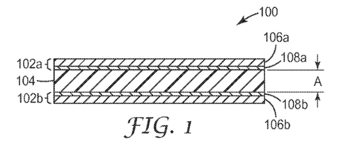
Fig. 1 is a schematic cross-sectional view of an exemplary embodiment of a
shielding article according to an aspect of the present invention.
Fig. 2 is a schematic cross-sectional view of another exemplary embodiment of
a
shielding article according to an aspect of the present invention.
Fig. 3 is a schematic cross-sectional view of another exemplary embodiment of
a
shielding article according to an aspect of the present invention.
Fig. 4 is a schematic cross-sectional view of another exemplary embodiment of
a
shielding article according to an aspect of the present invention.
Fig. 5 is a graph illustrating the improved shielding effectiveness achieved
by
shielding articles according to aspects of the present invention.
Fig. 6 is another graph illustrating the improved shielding effectiveness
achieved
by shielding articles according to aspects of the present invention.
DETAILED DESCRIPTION
In the following detailed description of the preferred embodiments, reference
is
made to the accompanying drawings that form a part hereof. The accompanying
drawings
show, by way of illustration, specific embodiments in which the invention may
be
practiced. It is to be understood that other embodiments may be utilized, and
structural or
logical changes may be made without departing from the scope of the present
invention.
The following detailed description, therefore, is not to be taken in a
limiting sense, and the
scope of the invention is defined by the appended claims.
In one aspect, the present invention includes a multi-layer shielding article
that is
useful for shielding of electronic communications devices by interfering with
or cutting
off the electrical or magnetic signal emitted from electromagnetic equipment,
electronics
equipment, receiving devices, or other external devices.
2
CA 02762218 2011-11-16
WO 2010/138348 PCT/US2010/035341
Fig. 1 illustrates an exemplary embodiment of a shielding article according to
an
aspect of the present invention. Shielding article 100 includes a first
conductive layer
102a and a second conductive layer 102b (collectively referred to herein as
"conductive
layers 102"). Second conductive layer 102b is spaced apart from first
conductive layer
102a by a non-conductive polymeric layer 104. "Non-conductive" is defined
herein as
substantially not electrically conductive. Polymeric layer 104 defines a
separation
distance A, which in this embodiment substantially corresponds with the
thickness of
polymeric layer 104. First conductive layer 102a and second conductive layer
102b
cooperatively provide a first shielding effectiveness. The first shielding
effectiveness is
based on a double-thickness single conductive layer which is effectively equal
to two
adjacent single-thickness conductive layers 102a and 102b. Unexpectedly, first
conductive layer 102a, second conductive layer 102b, and separation distance A
cooperatively provide a second shielding effectiveness that is greater than
the first
shielding effectiveness.
Conductive layers 102 may be formed by metalizing polymeric layer 104, such
as,
e.g., by chemical deposition (such as, e.g., electroplating), physical
deposition (such as,
e.g., sputtering), or any other suitable method. Alternatively, conductive
layers 102 may
be laminated onto polymeric layer 104. In one embodiment, conductive layers
102 each
have a thickness in the range of 100 to 30000 Angstroms (10 to 3000 nm). In
the
embodiment of Fig. 1, conductive layers 102a and 102b have substantially the
same
thickness. In other embodiments, conductive layers 102a and 102b may have a
different
thickness. Conductive layers 102 may include any suitable conductive material,
including
but not limited to copper, silver, aluminum, gold, and alloys thereof. First
conductive
layer 102a may include a different material or combination of materials than
second
conductive layer 102b. For example, first conductive layer 102a may include a
layer of
copper and second conductive layer 102b may include a layer of silver.
Polymeric layer 104 may include any suitable polymeric material, including but
not limited to polyester, polyimide, polyamide-imide, polytetrafluoroethylene,
polypropylene, polyethylene, polyphenylene sulfide, polyethylene naphthalate,
polycarbonate, silicone rubber, ethylene propylene diene rubber, polyurethane,
acrylate,
silicone, natural rubber, epoxies, and synthetic rubber adhesive. Polymeric
layer 104 may
include one or more additives and/or fillers to provide properties suitable
for the intended
3
CA 02762218 2011-11-16
WO 2010/138348 PCT/US2010/035341
application. Adhesive materials, additives, and fillers that may be included
in polymeric
layer 104 are described in more detail below. Polymeric layer 104 may include
non-
wovens, fabrics, foams, or a substantially hollow polymeric or adhesive layer.
In one
embodiment, polymeric layer 104 has a thickness in the range of 5 m to 500
m.
In the embodiment shown in Fig. 1, first and second conductive layers 102a and
102b each include a layer of copper 106a and 106b (collectively referred to
herein as
"copper layers 106"), respectively, disposed on a layer of nickel 108a andl08b
(collectively referred to herein as "nickel layers 108"), respectively (also
referred to as
"priming"). Nickel layers 108 and copper layers 106 are deposited using any
suitable
method known in the art. Polymeric layer 104 provides sufficient flexibility
for the final
use of shielding article 100, while it also has sufficient rigidity, thermal
stability, and
chemical stability, e.g., for use in the metal deposition process. Nickel
layers 108 provide
better adhesion of copper layers 106 to polymeric layer 104 than copper layers
106 alone.
Copper layers 106 provide sufficient electrical conductivity to allow the
construction to
act as a shielding article for use in mobile phones, televisions, gaming
electronics,
cameras, RFID security devices, medical devices, and electronic devices in
automotive
and aerospace applications, for example. In other embodiments, an additional
layer of
nickel may be deposited onto the outer surface of copper layers 106 to provide
corrosion
protection to copper layers 106. In one embodiment, nickel layers 108 each
have a
thickness in the range of 25 to 125 Angstroms (2.5 to 12.5 nm) and copper
layers 106 each
have a thickness in the range of 50 to 2000 Angstroms (5 to 200 nm). In a
preferred
embodiment, nickel layers 108 each have a thickness in the range of 50 to 100
Angstroms
(5 to 10 nm) and copper layers 106 each have a thickness in the range of 800
to 2000
Angstroms (80 to 200 nm). The preferred ranges of material thickness allow a
desired
balance of material flexibility and reliability, while providing adequate
amounts of
material for electrical conductivity and corrosion protection. Although in the
illustrated
embodiment, copper layers 106a and 106b have substantially the same thickness,
in other
embodiments, copper layers 106a and 106b may have a different thickness.
Similarly,
although in the illustrated embodiment, nickel layers 108a and 108b have
substantially the
same thickness, in other embodiments, nickel layers 108a and 108b may have a
different
thickness. Although in the illustrated embodiment, copper layers 106 are
deposited onto
nickel layers 108, in other embodiments, one or both of copper layers 106 may
be
4
CA 02762218 2011-11-16
WO 2010/138348 PCT/US2010/035341
deposited directly onto polymeric layer 104. Nickel layers 108 are defined
herein as
layers including at least one of nickel (Ni), nickel alloys, and austenitic
nickel-based
superalloys, such as, e.g., the austenitic nickel-based superalloy available
under the trade
designation INCONEL from Special Metals Corporation, New Hartford, New York,
U.S.A. Copper layers 106 are defined herein as layers including at least one
of copper
(Cu) and copper alloys.
Fig. 2 illustrates another exemplary embodiment of a shielding article
according to
an aspect of the present invention. Shielding article 200 includes shielding
article 100 as
described above and an adhesive layer 210 disposed on first conductive layer
102a. In
other embodiments, an adhesive layer 210 may be disposed on second conductive
layer
102b or on both first and second conductive layers 102a, 102b. In one
embodiment,
adhesive layer 210 is used to bond shielding article 200 to a protective
layer, or a device or
component that needs to be electromagnetically shielded, for example. Adhesive
layer
210 may include a pressure sensitive adhesive (PSA), a hot melt adhesive, a
thermoset
adhesive, a curable adhesive, or any other suitable adhesive. Adhesive layer
210 may
include one or more additives and/or fillers to provide properties suitable
for the intended
application. Adhesive materials, additives, and fillers that may be included
in adhesive
layer 210 are described in more detail below. Adhesive layer 210 may include a
corrosion
inhibitor. In one embodiment, adhesive layer 210 has a thickness in the range
of 10 m to
150 m.
Fig. 3 illustrates another exemplary embodiment of a shielding article
according to
an aspect of the present invention. Shielding article 300 includes shielding
article 200 as
described above and a protective layer 312 disposed adjacent adhesive layer
210. In this
embodiment, protective layer 312 is bonded to first conductive layer 102a by
adhesive
layer 210. In other embodiments, a protective layer 312 maybe disposed
adjacent second
conductive layer 102b or adjacent both first and second conductive layers
102a, 102b. In
one embodiment, protective layer 312 includes a polyester paper coated with an
inorganic
coating, such as, e.g., the polyester paper coated with an inorganic coating
available under
the trade designation TufQUIN from 3M Company, St. Paul, Minnesota, U.S.A.
TufQUIN offers the high-temperature capabilities of inorganic materials
combined with
the high mechanical strength gained by the use of organic fiber. TufQUIN
papers can be
combined with polyester film to form a flexible laminate uniquely suited for
high
5
CA 02762218 2011-11-16
WO 2010/138348 PCT/US2010/035341
temperature electrical insulation applications. In another embodiment,
protective layer
312 includes an aramid paper, such as, e.g., the aramid paper available under
the trade
designation NOMEX from E. I. du Pont de Nemours and Company, Wilmington,
Delaware, U.S.A. Protective layer 312 is typically capable of offering
chemical protection
(such as, e.g., protection against corrosion) as well as physical protection
(such as, e.g.,
protection against abrasion). Protective layer 312 may have any thickness
suitable for the
intended application.
Fig. 4 illustrates another exemplary embodiment of a shielding article
according to
an aspect of the present invention. Shielding article 400 includes a first
conductive layer
102a and a second conductive layer 102b as described above. Second conductive
layer
102b is spaced apart from first conductive layer 102a by a non-conductive
polymeric layer
404. Polymeric layer 404 defines a separation distance B, which in this
embodiment
substantially corresponds with the thickness of polymeric layer 404. First
conductive
layer 102a and second conductive layer 102b cooperatively provide a first
shielding
effectiveness. Unexpectedly, first conductive layer 102a, second conductive
layer 102b,
and separation distance B cooperatively provide a second shielding
effectiveness that is
greater than the first shielding effectiveness. Polymeric layer 404 includes a
first non-
conductive polymeric sublayer 414a, a second non-conductive polymeric sublayer
414b,
and a bonding adhesive layer 416 disposed between first polymeric sublayer
414a and
second polymeric sublayer 414b. In one embodiment, first and second polymeric
sublayers 414a and 414b are identical to polymeric layer 104 as described
above. A useful
advantage of this construction of polymeric layer 404 is in the method of
making shielding
article 400. In one embodiment, shielding article 400 is made as follows:
First,
conductive layer 102a is deposited onto first polymeric sublayer 414a, and
second
conductive layer 102b is deposited onto second polymeric sublayer 414b,
resulting in two
separate constructions. Then, bonding adhesive layer 416 is laminated to first
polymeric
sublayer 414a, and second polymeric sublayer 414b is laminated to bonding
adhesive layer
416, combining the two separate constructions into shielding article 400.
Bonding
adhesive layer 416 may include a pressure sensitive adhesive (PSA), a hot melt
adhesive, a
thermoset adhesive, a curable adhesive, or any other suitable adhesive.
Bonding adhesive
layer 416 may include one or more additives and/or fillers to provide
properties suitable
for the intended application. Adhesive materials, additives, and fillers that
may be
6
CA 02762218 2011-11-16
WO 2010/138348 PCT/US2010/035341
included in bonding adhesive layer 416 are described in more detail below.
Adhesive
layers of a shielding article according to an aspect of the present invention,
such as, e.g.,
adhesive layers 210 and 416, may include any of the various types of materials
used for
bonding, adhering, or otherwise affixing one material or surface to another.
Classes of
adhesives include, for instance, pressure sensitive adhesives, hot melt
adhesives, thermoset
adhesives, and curable adhesives. The pressure sensitive adhesives include
those based on
silicone polymers, acrylate polymers, natural rubber polymers, and synthetic
rubber
polymers. They may be tackified, crosslinked, and/or filled with various
materials to
provide desired properties. Hot melt adhesives become tacky and adhere well to
substrates when they are heated above a specified temperature and/or pressure;
when the
adhesive cools down, its cohesive strength increases while retaining a good
bond to the
substrate. Examples of types of hot melt adhesives include, but are not
limited to,
polyamides, polyurethanes, copolymers of ethylene and vinyl acetate, and
olefinic
polymers modified with more polar species such as maleic anhydride. Thermoset
adhesives are adhesives that can create an intimate contact with a substrate
either at room
temperature or with the application of heat and/or pressure. With heating, a
chemical
reaction occurs in the thermoset to provide long term cohesive strength at
ambient,
subambient, and elevated temperatures. Examples of thermoset adhesives include
epoxies,
silicones, and polyesters, and polyurethanes. Curable adhesives can include
thermosets,
but are differentiated here in that they can cure at room temperature, either
with or without
the addition of external chemical species or energy. Examples include two-part
epoxies
and polyesters, one-part moisture cure silicones and polyurethanes, and
adhesives utilizing
actinic radiation to cure such as UV, visible light, or electron beam energy.
Non-conductive polymeric layers and adhesive layers of a shielding article
according to an aspect of the present invention, such as, e.g., polymeric
layer 104,
polymeric sublayers 414a and 414b, and adhesive layers 210 and 416, may
include various
types of additives and fillers alone or in combination to provide properties
suitable for the
intended application. Typical additives and fillers include plasticizers,
thermal stabilizers,
antioxidants, UV stabilizers, pigments, dyes, flame retardants, smoke
suppressants,
conductive fillers, species to improve chemical resistance, and other property
modifiers.
Flame retardants represent another class of filler useful for some
applications to
ensure that the overall product construction minimizes, ameliorates, or
eliminates the
7
CA 02762218 2011-11-16
WO 2010/138348 PCT/US2010/035341
propagation of fire. Types of flame retardants can include halogenated flame
retardants
such as decabromo dipehnyl oxide, chlorinated paraffin wax, brominated
phenols, and
brominated bisphenol A. Furthermore, formulations which employ halogenated
flame
retardants often include antimony oxides such as antimony trioxide which act
synergistically to enhance the flame retarding abilities of the halogen
compound.
Another type of flame retardant relies on intumescence or char formation to
reduce
the polymer flammability and block combustion. Some examples of intumescent
flame
retardants include phosphates such as ammonium polyphosphate and nitrogen
compounds
such as melamine. Another class of flame retardant block flame propagation by
generating inert gasses and promoting char formation upon decomposition. These
include
inorganic hydroxides, hydroxycarbonates and carbonates such as aluminum
trihydrate,
magnesium hydroxide and magnesium carbonate.
Other classes of flame retardants include molybdenates and borates which also
suppress smoke generation. Some examples of these types of flame retardants
include
ammonium octomolybdenate and zinc borate. Any combination of these and other
well
known flame retardants may be included.
Other types of fillers that may be included, e.g., to enhance overall
performance or
reduce cost, include titanium dioxide, fumed silica, carbon fibers, carbon
black, glass
beads, glass fibers, glass bubbles, mineral fibers, clay particles, organic
fibers, zinc oxide,
aluminum oxide, boron nitride, aluminum nitride, barium titanate, molybdenum
and the
like.
One important filler useful for some shielding applications is a conductive
particle
to provide the flow of electrical current from the shielding layer to a ground
plane. The
conductive particles can be any of the types of particles currently used, such
as spheres,
flakes, rods, cubes, amorphous, or other particle shapes. They may be solid or
substantially solid particles such as carbon black, carbon fibers, nickel
spheres, nickel
coated copper spheres, metal-coated oxides, metal-coated polymer fibers, or
other similar
conductive particles. These conductive particles can be made from electrically
insulating
materials that are plated or coated with a conductive material such as silver,
aluminum,
nickel, or indium tin-oxide. The metal-coated insulating material can be
substantially
hollow particles such as hollow glass spheres, or may comprise solid materials
such as
glass beads or metal oxides. The conductive particles may be on the order of
several tens
8
CA 02762218 2011-11-16
WO 2010/138348 PCT/US2010/035341
of microns to nanometer sized materials such as carbon nanotubes. The
conductive
adhesive can also be comprised of a conductive polymeric matrix.
Shielding articles according to aspects of the present invention have numerous
advantages for their intended use as compared to conventional shielding
articles. One
particular advantage is an unexpected performance in electromagnetic
shielding, which is
described in greater detail below.
Examples
Shielding effectiveness measurements on shielding articles according to
aspects of
the present invention and on conventional shielding articles were conducted.
The
shielding effectiveness measurements were conducted generally following the
Standard
Test Method for Measuring the Electromagnetic Shielding Effectiveness of
Planar
Materials ASTM D 4935-99. Measurements were performed on an Agilent
Technologies
N5230A PNA-L Network Analyzer outfitted with a TEM cell, and the IF Bandwidth
and
number of scans averaged were adjusted as necessary to accurately measure the
shielding
level of the various samples. The following test samples were prepared.
Comparative test sample C501 was a sample of a conventional shielding article
including a single conductive layer deposited onto a non-conductive polymeric
layer.
Specifically, comparative test sample C501 was created as follows: A layer of
nickel
having a thickness of about 75 Angstroms (7.5 nm) was deposited onto a
polymeric layer
including polyethylene terephthalate and having a thickness of about 2.0 mil
(51 m). A
layer of copper having a thickness of about 1100 Angstroms (110 nm) was
deposited onto
the layer of nickel.
Test sample 502 was a sample of a shielding article according to an aspect of
the
present invention. Specifically, test sample 502 was created as follows: A
layer of nickel
having a thickness of about 75 Angstroms (7.5 nm) was deposited onto a
polymeric layer
including polyethylene terephthalate and having a thickness of about 2.0 mil
(51 m). A
first layer of copper having a thickness of about 550 Angstroms (55 nm) was
deposited
onto the layer of nickel. A second layer of copper having a thickness of about
550
Angstroms (55 nm) was deposited onto the opposing surface of the polymeric
layer.
Test sample 503 was a sample of another shielding article according to an
aspect of
the present invention. Specifically, test sample 503 was created as follows: A
first layer
of nickel having a thickness of about 75 Angstroms (7.5 nm) was deposited onto
a first
9
CA 02762218 2011-11-16
WO 2010/138348 PCT/US2010/035341
polymeric layer including polyethylene terephthalate and having a thickness of
about 2.0
mil (51 m). A first layer of copper having a thickness of about 550 Angstroms
(55 nm)
was deposited onto the first layer of nickel. A second layer of nickel having
a thickness of
about 75 Angstroms (7.5 nm) was deposited onto a second polymeric layer
separate from
the first polymeric layer. A second layer of copper having a thickness of
about 550
Angstroms (55 nm) was deposited onto the second layer of nickel. A bonding
adhesive
layer including an acrylate pressure sensitive adhesive and having a thickness
of about 1.0
mil (25 m) was laminated to the first polymeric layer. The second polymeric
layer was
laminated to the bonding adhesive layer.
Test sample 504 was a sample of another shielding article according to an
aspect of
the present invention. Specifically, test sample 504 was created as follows: A
first layer
of nickel having a thickness of about 75 Angstroms (7.5 nm) was deposited onto
a first
polymeric layer including polyethylene terephthalate and having a thickness of
about 2.0
mil (51 m). A first layer of copper having a thickness of about 550 Angstroms
(55 nm)
was deposited onto the first layer of nickel. A second layer of nickel having
a thickness of
about 75 Angstroms (7.5 nm) was deposited onto a second polymeric layer
separate from
the first polymeric layer. A second layer of copper having a thickness of
about 550
Angstroms (55 nm) was deposited onto the second layer of nickel. A bonding
adhesive
layer including an acrylate pressure sensitive adhesive and having a thickness
of about 5.0
mil (127 m) was laminated to the first polymeric layer. The second polymeric
layer was
laminated to the bonding adhesive layer.
Table 1
Separation Additional
Number of Average Shielding
Specimen Copper Layering Between Shielding Compared to
Averaged Copper er Layers (dB) Sample C501
(dB)
Sample C501 6 Single Layer 0 -55.7 N/A
1100 Angstroms
Sample 502 6 Dual Layer 51 -66.9 -11.2
550 Angstroms Each
Sample 503 4 Dual Layer 127 -71.4 -15.7
550 Angstroms Each
Sample 504 3 Dual Layer 229 -78.4 -22.7
550 Angstroms Each
CA 02762218 2011-11-16
WO 2010/138348 PCT/US2010/035341
Table 1 and Fig. 5 present the shielding data, averaged from 100 to 1000 MHz
for
samples C501-504. The shielding effectiveness of comparative test sample C501
was
measured at -55.7 dB over the range of 100 through 1000 MHz. By effectively
dividing in
half and spacing apart the single layer of copper of comparative test sample
C501 by a
separation distance of about 51 m, resulting in a construction substantially
identical to
that of test sample 502, the shielding effectiveness was unexpectedly
increased to -66.9 dB
(-11.2 dB additional shielding). This data illustrates that the presence of a
separation
distance between conductive layers of a shielding article unexpectedly
increases the
shielding effectiveness of the shielding article. By increasing the separation
distance to
about 127 m (test sample 503) and 229 m (test sample 504), the shielding
effectiveness
was further increased to -71.4 dB (-15.7 dB additional shielding) and -78.4 dB
(-22.7 dB
additional shielding), respectively. This data illustrates that as the
separation distance is
increased, the shielding effectiveness increases. Fig. 5 further illustrates
that in the limit
as the layer separation decreases towards zero, the extrapolated value (y-
intercept) is not
zero. This demonstrates the unexpected synergy of utilizing dual layer
shielding layers
versus a single layer having substantially the same effective thickness.
Additional shielding effectiveness measurements on shielding articles
according to
aspects of the present invention and on conventional shielding articles were
conducted.
The shielding effectiveness measurements were conducted as described above.
The
following test samples were prepared.
Comparative test sample C601 was a sample of a conventional shielding article
including a single conductive layer including an aluminum foil having a
thickness of about
0.9 mil (23 m).
Test sample 602 was a sample of a shielding article according to an aspect of
the
present invention. Specifically, test sample 602 was created as follows: A
first
conductive layer including an aluminum foil having a thickness of about 0.4
mil (10 m)
was laminated to a polymeric layer including acrylate bonding adhesive having
a thickness
of about 1.0 mil (25 m). A second conductive layer including an aluminum foil
having a
thickness of about 0.4 mil (10 m) was laminated to the opposing surface of
the polymeric
layer.
Test sample 603 was a sample of a shielding article according to an aspect of
the
present invention. Specifically, test sample 603 was created as follows: A
first
11
CA 02762218 2011-11-16
WO 2010/138348 PCT/US2010/035341
conductive layer including an aluminum foil having a thickness of about 0.4
mil (10 m)
was laminated to a polymeric layer including acrylate bonding adhesive having
a thickness
of about 2.0 mil (51 m). A second conductive layer including an aluminum foil
having a
thickness of about 0.4 mil (10 m) was laminated to the opposing surface of
the polymeric
layer.
Test sample 604 was a sample of a shielding article according to an aspect of
the
present invention. Specifically, test sample 604 was created as follows: A
first
conductive layer including an aluminum foil having a thickness of about 0.4
mil (10 m)
was laminated to a polymeric layer including acrylate bonding adhesive having
a thickness
of about 4.0 mil (102 m). A second conductive layer including an aluminum
foil having
a thickness of about 0.4 mil (10 m) was laminated to the opposing surface of
the
polymeric layer.
Test sample 605 was a sample of a shielding article according to an aspect of
the
present invention. Specifically, test sample 605 was created as follows: A
first
conductive layer including an aluminum foil having a thickness of about 0.4
mil (10 m)
was laminated to a polymeric layer including acrylate bonding adhesive having
a thickness
of about 6.0 mil (152 m). A second conductive layer including an aluminum
foil having
a thickness of about 0.4 mil (10 m) was laminated to the opposing surface of
the
polymeric layer.
Table 2
Separation Additional
Number of Between Average Shielding
Specimen Aluminum Layering Aluminum Layers Shielding Compared to
Averaged ( m) (dB) Sample C601
(dB)
Sample C601 2 23 Single Layer 0 -112.1 N/A
Sample 602 2 Dual Layer 25 -123.4 -11.3
10 m Each
Sample 603 2 Dual Layer 51 -123.6 -11.4
10 m Each
Sample 604 2 Dual Layer 102 -126.4 -14.2
10 m Each
Sample 605 2 Dual Layer 152 -128.4 -16.2
10 m Each
Table 2 and Fig. 6 present the shielding data, averaged from 100 to 1000 MHz
of
samples C601-605. The shielding effectiveness of comparative test sample C601
was
measured at -112.1 dB over the range of 100 through 1000 MHz. By effectively
dividing
12
CA 02762218 2011-11-16
WO 2010/138348 PCT/US2010/035341
in half and spacing apart the single layer of aluminum of comparative test
sample C601 by
a separation distance of about 25 m, resulting in a construction
substantially identical to
that of test sample 602, the shielding effectiveness was unexpectedly
increased to -123.4
dB (-11.3 dB additional shielding). This data illustrates that the presence of
a separation
distance between conductive layers of a shielding article unexpectedly
increases the
shielding effectiveness of the shielding article. By increasing the separation
distance to
about 51 m (test sample 603), 102 m (test sample 604), and 152 m (test
sample 605),
the shielding effectiveness was further increased to -123.6 dB (-11.4 dB
additional
shielding), -126.4 dB (-14.2 dB additional shielding), and -128.4 dB (-16.2 dB
additional
shielding), respectively. This data illustrates that as the separation
distance is increased,
the shielding effectiveness increases. Fig. 6 further illustrates that in the
limit as the layer
separation decreases towards zero, the extrapolated value (y-intercept) is not
zero. This
demonstrates the unexpected synergy of utilizing dual layer shielding layers
versus a
single layer having substantially the same effective thickness.
In combination, the data presented in Tables 1-2 and Figs. 5-6 illustrates
that
additional shielding effectiveness can be achieved in shielding articles
according to
aspects of the present invention including first and second conductive layers
including
different conductive materials.
Additional shielding effectiveness measurements on shielding articles
according to
an aspect of the present invention were conducted. The shielding effectiveness
measurements were conducted as described above. The following test sample was
prepared.
Test sample 701 was a sample of a shielding article according to an aspect of
the
present invention. Specifically, test sample 701 was created as follows: A
layer of nickel
having a thickness of about 150 Angstroms (15 nm) was deposited onto a
polymeric layer
including polyethylene terephthalate and having a thickness of about 2.0 mil
(51 m). A
layer of copper having a thickness of about 1800 Angstroms (180 nm) was
deposited onto
the layer of nickel. A layer of titanium having a thickness of about 150
Angstroms (15
nm) was deposited onto the opposing surface of the polymeric layer. A layer of
silver
having a thickness of about 1000 Angstroms (100 nm) was deposited onto the
layer of
titanium. The average shielding effectiveness of test sample 701 was measured
at -81.6
dB, whereby 4 specimens were averaged. This example demonstrates that a
shielding
13
CA 02762218 2011-11-16
WO 2010/138348 PCT/US2010/035341
article wherein a first conductive layer and a second conductive layer include
different
conductive materials can be utilized effectively. It also demonstrates that
the thickness of
the first and second conductive layers may be different.
It has been demonstrated that a shielding article including a first conductive
layer
spaced apart from a second conductive layer (i.e., dual layer construction)
has a greater
shielding effectiveness than a shielding article wherein the first conductive
layer and the
second conductive layer essentially form a single conductive layer (i.e.,
single layer
construction). Based on this, a person of ordinary skill in the art will
easily understand
that a shielding article including a plurality conductive layers, each
conductive layer
spaced apart from an adjacent conductive layer (i.e., multi-layer
construction) will have a
greater shielding effectiveness than a shielding article wherein the
conductive layers form
a single conductive layer (i.e., single layer construction). For example, in a
shielding
article including a first conductive layer spaced apart from a second
conductive layer, by
dividing in half and separating one or both of first and second conductive
layers (resulting
in a three- or four-layer construction), the shielding effectiveness of the
shielding article
will further increase.
Although specific embodiments have been illustrated and described herein for
purposes of description of the preferred embodiment, it will be appreciated by
those of
ordinary skill in the art that a wide variety of alternate and/or equivalent
implementations
calculated to achieve the same purposes may be substituted for the specific
embodiments
shown and described without departing from the scope of the present invention.
Those
with skill in the mechanical, electro-mechanical, and electrical arts will
readily appreciate
that the present invention may be implemented in a very wide variety of
embodiments.
This application is intended to cover any adaptations or variations of the
preferred
embodiments discussed herein. Therefore, it is manifestly intended that this
invention be
limited only by the claims and the equivalents thereof.
14