Note: Descriptions are shown in the official language in which they were submitted.
CA 02762332 2011-12-15
242051
HUB UNIT FOR A HIGH TEMPERATURE ELECTRONIC
MONITORING SYSTEM
BACKGROUND OF THE INVENTION
The present invention generally relates to electronic equipment, and more
particularly to
electronic hardware capable of operating within a high temperature
environment, such as
on or adjacent a gas turbine engine.
Aircraft gas turbine engines undergo testing during their development, as well
as during
production and subsequent servicing. Numerous engine performance parameters
are
typically monitored to assess the performance of an engine, including various
temperatures, pressures, flow rates, forces, rotational speeds, etc. As
nonlimiting
examples, it is typically desirable to monitor engine inlet, compressor and
exhaust gas
temperatures, pressures within the fan, compressor and turbine sections, fuel
and airflow
rates, compressor and fan rotor speeds, blade tip clearances, mechanical
stresses and part
vibrations. Development and flight test aircraft engines may be required to
have
thousands of sensors to monitor the various parameters of interest.
Engine testing is typically conducted on a stationary test stand that is often
located
outdoors. A nonlimiting example of such a test stand 100 is schematically
represented in
FIG. 1. The stand 100 is represented as including a vertical support column
102 mounted
to a foundation 104 in the ground, and a head (thrust) frame 106 mounted on
the column
102 from which an aircraft engine 108 is mounted for testing. The head frame
106
includes an adapter 110 to which the engine 108 is attached with a pylon 112
that is
appropriately configured for the particular engine 108.
During engine testing, the engine 108 and its immediate surroundings can reach
very high
temperatures. For example, temperatures may approach or exceed 260 C
surrounding the
-1-
CA 02762332 2011-12-15
242051
engine core beneath the engine cowling (nacelle) 114, as well as on the head
frame 106
and its adapter 110. While sensors used to monitor the engine 108 have been
developed
to withstand these temperatures, the electronics used to process the sensor
data have been
limited to much lower temperatures. For example, typical commercial electronic
components are often limited to about 85 C, and even military standard
components are
typically rated to not higher than 125 C. As such, each sensor typically
requires a
separate continuous wire or tube to carry its output signal to a remote data
acquisition
system, which is often located within an enclosed facility equipped with a
controlled
environment. The facility may be a considerable distance from the engine test
stand, for
example, 50 meters to in excess of 300 meters. Routing, managing and
maintaining the
numerous (potentially thousands) of data wires and tubes requires a
considerable effort.
Consequently, the ability to reduce the length and number of wires and tubes
would be
helpful and beneficial.
BRIEF DESCRIPTION OF THE INVENTION
The present invention provides a hub unit adapted for use in a monitoring
system adapted
to monitor engine performance parameters of a gas turbine engine operating on
a
stationary test stand, or during on-wing flight test, or during normal
aircraft operation,
and particularly a monitoring system comprising sensors mounted on the engine
for
sensing the engine performance parameters and generating digital sensor
outputs.
According to a first aspect of the invention, the hub unit includes a housing,
at least one
signal conditioning circuit board within the housing and adapted to receive
the analog
sensor outputs from the sensors, and a control circuit board within the
housing, connected
to the signal conditioning circuit board, and adapted to produce digital data
corresponding
to analog sensor outputs. The control circuit board and the signal
conditioning circuit
board each comprise electrical circuit components that define an analog signal
processing
path and have accuracy and precision characteristics that drift in response to
component
aging and to changes in the temperature to which the hub unit is subjected.
The hub unit
further includes means for performing a continuous calibration scheme by
periodically
-2-
CA 02762332 2011-12-15
242051
applying a reference voltage and a zero voltage to the signal conditioning
circuit board to
determine and remove errors in the analog signal processing path resulting
from the drifts
of the electrical circuit components of the control circuit board and the
signal
conditioning circuit board.
According to a second aspect of the invention, in addition to certain aspects
recited
above, the hub unit may further include means on the signal conditioning
circuit board for
multiplexing a plurality of the analog sensor outputs generated by the sensors
to produce
an individual multiplexed analog output, and at least one amplifier with
adjustable gain
for scaling the analog sensor outputs of the individual multiplexed analog
output to
produce an individual conditioned multiplexed analog output from which the
corresponding digital data are produced. The amplifier and the adjustable gain
thereof
are controlled by the control circuit board.
A technical effect of the invention is the ability of the hub unit to operate
at high
temperatures, for example, higher temperatures than possible with more
temperature-
sensitive hardware of the type conventionally used to process digital data. As
such, data
processing can be performed at a location remote from the high temperature
environment
being monitored. On the other hand, the hub unit and particularly its control
and signal
conditioning circuit boards can be specially adapted for high temperature
operation,
preferably without the use of active cooling. Furthermore, the continuous
calibration
scheme removes errors that would otherwise exist in the analog signal
processing path as
a result of the accuracy and precision characteristics of the electrical
circuit components
of the control circuit board and the signal conditioning circuit board tending
to drift due
to component aging and the high temperature environment of the hub unit. In
accordance
with the second aspect of the invention, the multiplexing capability can
reduce the
number of wires or cables necessary to transmit data to the remotely-located
distributor
unit.
Other aspects and advantages of this invention will be better appreciated from
the
following detailed description.
-3-
CA 02762332 2011-12-15
242051
BRIEF DESCRIPTION OF THE DRAWINGS
FIG. 1 is a schematic representation of a test stand for a gas turbine engine.
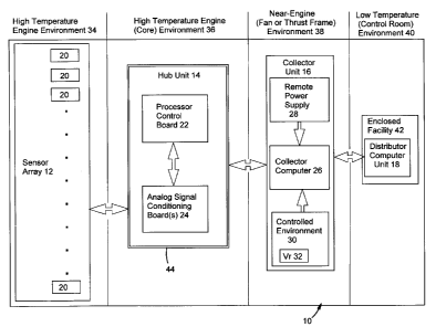
FIG. 2 is a block diagram representing tiered units of a monitoring system
adapted for
monitoring performance parameters of a gas turbine engine operating while
mounted on a
test stand, such as of the type represented in FIG. 1.
FIG. 3 is a block diagram representing certain components of the monitoring
system of
FIG. 2, including details of a processor control board of the monitoring
system.
FIG. 4 is a block diagram representing an analog signal conditioning board of
the
monitoring system of FIG. 2.
FIG. 5 schematically represents a voltage reference device for use with a
collector
computer of the monitoring system of FIG. 2.
DETAILED DESCRIPTION OF THE INVENTION
FIG. 2 is a block diagram representing various units of a monitoring system 10
adapted
for monitoring performance parameters of a gas turbine engine while the engine
is
mounted and operating on a stationary test stand, for example, the test stand
100
represented in FIG. 1. The system 10 can also be used to monitor an engine
during on-
wing flight tests, as well as during normal aircraft operation. While the
monitoring
system 10 is particularly well suited for monitoring a gas turbine engine, and
for
convenience will be described in reference to the engine 108 and its stand 100
represented in FIG. 1, the use of the system 10 is not limited to such
applications.
Instead, the system 10 is more broadly applicable to a wide variety of
situations in which
there is a desire or need to monitor performance parameters of an apparatus
operating in
an environment subjected to elevated temperatures.
As represented in FIG. 2, the system 10 is generally identified as having
units 12, 14, 16
and 18 that are located in four environments 34, 36, 38 and 40 with respect to
the gas
-4-
CA 02762332 2011-12-15
242051
turbine engine 108. The first unit 12 comprises an array of sensors 20
appropriately
located in and around the engine 108 to monitor performance parameters of the
engine
108 for the purpose of assessing the performance of the engine. Any number of
sensors
20 may be employed by the system 10, and the sensors 20 may be of various
types, for
example, to monitor temperatures, pressures, flow rates, forces, rotational
speeds, etc., of
the engine 108, as was previously discussed in reference to FIG. 1. Certain
types of
sensors 20 are typically employed in large numbers during the monitoring of
engine
operation, including thermocouples, resistance temperature detectors (RTDs),
and
pressure transducers. Because the sensors 20 are located to directly detect
the parameters
of interest, the unit (array) 12 of sensors 20 is indicated in FIG. 2 as being
located in a
"high temperature engine environment" 34, where maximum temperatures exceeding
200 C are often encountered by the system 10 and may reach as high as 260 C or
more.
Suitable sensors 20 for use in the system 10 are commercially available and
commonly
used for monitoring gas turbine engine parameters, and therefore will not be
discussed in
any detail here. The particular output signals generated by the sensors 20
will depend on
the type of sensors 20 used, though in most cases the signals will be analog
signals that
must be digitized in order for their data to be used by computer processing
equipment to
assess the performance of the engine.
The remaining primary units 14, 16 and 18 of the system 10 are identified in
FIG. 2 as
located in environments 36, 38 and 40 where lower temperatures are likely to
occur. A
first of these units will be referred to as a hub unit 14, with which the
sensors 20 directly
communicate through any suitable wires, tubes, or other appropriate connectors
commonly employed with the particular type of sensors 20 used. The hub unit 14
represented in FIG. 2 will typically be one of a number of hub units 14 that
may be used
in the system 10, depending on the number of sensors 20 and the number of
sensors 20
each hub unit 14 can manage. Similar to the environment 34 for the sensors 20,
the
environment 36 for the hub unit 14 is identified as a "high temperature engine
environment" 34, in that the hub units 14 are adapted to be located in close
proximity to
the engine 108, for example, within about three meters of the engine 108, such
as the
-5-
CA 02762332 2011-12-15
242051
engine core environment beneath the engine cowling 114. In addition to
locations
directly on the engine 108 and beneath its cowling 114, other locations may
include
adjacent locations on the head frame 106 or adapter 110 of the stand 100,
where very
high temperatures are still likely to be encountered by the system 10. For
example,
temperatures beneath the cowling 114 and adjacent locations on the head frame
106 or
adapter 110 often exceed 125 C, and can reach much higher temperatures, for
example,
higher than 200 C and potentially as high as 260 C or more. Consequently,
electronic
components of the hub units 14 must be capable of withstanding significantly
higher
temperatures than is possible with conventional electronic components and even
military
standard components.
In contrast, the environments 38 and 40 for the remaining two units 16 and 18
of the
system 10, referred to as a collector unit 16 and a distributor unit 18, are
identified as a
"near-engine environment" 38 and a "low temperature environment" 40. The
former is
designated as such because the collector unit 16 is adapted to be located in
proximity to
the engine 108 but not as close to the engine core as the hub units 14. For
example, the
collector unit 16 may be located within the engine fan case environment or on
the stand
100, such as on the head (thrust) frame 106, at distances of about three to
ten meters from
the core of the engine 108. At these locations, temperatures will usually
exceed 55 C,
but are significantly less than 260 C and typically less than 125 C.
Consequently,
electronic components of the collector unit 16 must typically be capable of
withstanding
high temperatures, though not as high as the hub units 14. In some situations,
military
standard components rated up to 125 C may be used, and possibly conventional
electronic components rated up to 85 C.
On the other hand, the low temperature environment 40 of the distributor unit
18 permits
the use of conventional electronic components rated at no more than 85 C. The
environment 40 is designated as "low temperature" in that the distributor unit
18 can be
and preferably is located in a controlled-temperature environment, for
example, an
enclosed facility that is near the test stand 100 and is stabilized with air-
conditioning to
-6-
CA 02762332 2011-12-15
242051
maintain a temperature of less than 55 C. For on-wing engine operation, the
environment 40 may be within the aircraft. The distributor unit 18 preferably
has the
most processing power of the system 10, and therefore will typically comprise
one or
more computer servers, personal computers, and/or other processing equipment
adapted
for data processing, collectively represented by a distributor computer 42 in
FIG. 2. In
addition to a real-time calibration functionality discussed below, the
distributor computer
42 may also provide the capability of engineering unit conversion, system
configuration,
and database functionality. Suitable equipment for the distributor computer 42
are likely
to be relatively sensitive to temperature, and therefore benefit from being
housed at
roughly room temperature. The low temperature environment 40 is typically
remotely
located from the engine test stand 100, for example, in excess of fifty
meters.
FIG. 2 schematically represents the hub unit 14 as comprising a processor
control board
22 and one or more analog signal conditioning boards 24. These boards 22 and
24 are
preferably enclosed in a housing 44, schematically represented in FIG. 2 as
completely
surrounding and enclosing the boards 22 and 24. The processor control board 22
and
analog signal conditioning boards 24 operate together to convert the analog
output signals
of the sensors 20 to digital data that can be processed by the distributor
unit 18.
According to certain preferred aspects of the invention, the processor control
board 22
and analog signal conditioning boards 24 also combine to perform additional
processes to
ensure the integrity of the analog output signals received from the sensors 20
prior to
their analog-digital conversion. As will be explained in more detail below,
one such
additional process is to provide a continuous calibration feature that detects
any drift in
the accuracy and precision characteristics of the electronic components of the
analog
signal conditioning boards 24 and the processor control board 22 that can
result from
component aging and variations in temperature, such as the extreme temperature
changes
to which the hub unit 14 is subjected. The calibration feature produces
calibration data
that can be used by the distributor computer 42 to perform real-time
corrections of the
digital data acquired from the hub unit 14 via the collector unit 16, and more
particularly
a collector computer 26 of the unit 16. Another preferred process is to
multiplex the
-7-
CA 02762332 2011-12-15
242051
analog output signals of multiple sensors 20 into multiplexed analog outputs,
thereby
reducing the number of connections required to transmit the digital data to
the collector
unit 16 over, for example, a serial data connector such as an RS-485 serial
communications cable. Still another preferred process is to interleave the
multiplexed
analog outputs of one group (bank) of sensors 20 with the multiplexed analog
outputs of
other banks of sensors 20, so that the individual analog output signals of the
multiplexed
analog outputs more quickly "settle" between the sets of outputs. These and
other aspects
of the hub unit 14 will be discussed in further detail below.
The collector hub 16 is schematically represented in FIG. 2 as comprising the
collector
computer 26, a power supply 28, and a temperature-controlled environment 30
that
contains a system voltage reference device 32, as will be explained in more
detail below.
The primary function of the power supply 28 is to supply power to the
electronic
components of the system 10, including the sensors 20 (as may be required) and
the
electronic components housed in the hub unit 14. A preferred power supply 28
is a dual
topology design with a switching regulator front end and linear regulator back
end. The
power supply 28 may be configured to generate multiple independently-regulated
voltages for each hub unit 14 to increase system fault tolerance and decrease
noise
coupling. The collector computer 26 receives the digital data from the hub
unit 14, as
well as any additional hub units 14 contained in the system 10, prior to
forwarding the
digital data to the distributor computer 42 of the distributor unit 18. The
collector
computer 26 is preferably configured to have a logging capability for
synchronizing the
flow of the digital data to the distributor computer 42, for example,
utilizing inter-range
instrumentation group (IRIG) time codes or a Network Time Protocol (NTP). More
particularly, the collector computer 26 preferably operates as an intelligent
switch for the
incoming digital data from multiple hub units 14 by accurately time stamping
multiple
streams of digital data coming from the hub units 14, packing the data into
frames, and
then transmitting the data to the distributor computer 42, for example, over a
fiber-based
Ethernet connection. Suitable components for time stamping multiple data
streams and
packing data into frames are well known in the art, and therefore will not be
discussed in
-8-
CA 02762332 2011-12-15
242051
any detail here. The use of a fiber optic cable for the data connection
between the
collector computer 26 and the distributor computer 42 is preferred for the
purpose of
reducing the susceptibility of the transmission to lightening, which is
desirable since the
transmission cable will typically be exposed to an outdoor environment as a
result of
being routed between the test stand 100 and the remote facility housing the
distributor
unit 18. The collector computer 26, power supply 28 and controlled environment
30 may
all be enclosed within a suitable protective housing (not shown) that protects
these
components from direct exposure to the elements.
Notably, because of multiplexing at the level of the hub units 14 and
synchronization at
the level of the collector unit 16, the digital data can be supplied to the
distributor unit 18
over a single Ethernet connection, which is in stark contrast to the typical
thousands of
cables and tubes previously required to transmit sensor output to a remote
data
acquisition system of the prior art.
FIG. 3 is a block diagram representing the processor control board 22, some of
its
components, and its connection to the analog signal conditioning boards 24 and
the
collector unit 16. The processor control board 22 is represented as being
equipped with a
microprocessor 46 adapted to run from a program stored in ROM (read-only
memory) 48,
such as an EEPROM (electrically-erasable programmable read only memory), and
uses
RAM (random access memory) 50 to store the digital data generated from the
sensors 20,
as well as any variables used in calculations performed by the control board
22. The
microprocessor 46 preferably performs a gain setting function associated with
the signal
conditioning boards 24 (discussed below), controls/selects which individual or
blocks of
signal channels of the sensors 20 are read, the timing of the data
acquisition, error
sensing, analog-to-digital conversion, execution of any built-in test (BIT)
modes, sensor
adaptation (based on the types of sensors 20), and the collection, formatting
and transfer
of the digital data to the collector computer 26. As indicated in FIG. 3, the
input/output
(I/O) functions of the board 22 are preferably directed in the form of memory
mapped I/O
operations. As also seen in FIG. 3, the processor control board 22 also
transmits zero and
-9-
CA 02762332 2011-12-15
242051
full-scale control outputs to the analog signal conditioning boards 24, as
well as directly
communicates with the collector computer 26. As will be discussed in reference
to the
conditioning boards 24 and FIG. 4, the zero and full-scale control outputs
transmitted by
the control board 22 are part of a continuous calibration scheme that
periodically applies
a zero voltage and reference voltage to detect and compensate for any drift in
the
accuracy and precision characteristics of the electronic components of the
conditioning
boards 24 resulting from variations in temperature and component aging.
As previously noted, the hub unit 14 is intended to operate at temperatures
greater than
125 C, and preferably as high as at least 200 C. In preferred embodiments, the
microprocessor 46, ROM 48, RAM 48 and passive components mounted to the
control
board 22 are capable of operating at temperatures above 200 C. To achieve this
capability, the microprocessor 46, ROM 48 and RAM 48 are preferably
implemented
with silicon-on-insulator (SOI) substrates and processing technology. As known
in the
art, SOI substrates typically comprise a thin epitaxial layer on an insulator.
The substrate
is typically formed by oxidizing one or both bonding surfaces of a pair of
semiconductor
(e.g., silicon) wafers prior to bonding the wafers. Most typically, a single
silicon dioxide
layer is grown on an epitaxial layer formed on a silicon wafer. After bonding
the wafers,
all but the insulator and epitaxial layer (and optionally the silicon layer of
the second
wafer) are etched away, such that the silicon dioxide layer forms an insulator
that
electrically isolates the epitaxial layer. A commercial example of a solid-
state
microprocessor implemented on an SOI substrate using SOI processing technology
is the
HT83C51 microprocessor commercially available from Honeywell. Commercial
examples of RAM components implemented on SOI substrates include the HT6256
256Kbit SRAM component available from Honeywell, and commercial examples of
ROM components implemented on SOI substrates include ROM components from
Twilight Technology Inc.
The substrate on which the electronic components of the processor control
board 22 are
mounted is also preferably capable of withstanding temperatures of at least
260 C. A
-10-
CA 02762332 2011-12-15
242051
preferred high-temperature substrate material is commercially available from
Rogers
Corporation under the name R04003C, which is a glass-reinforced
hydrocarbon/ceramic
laminate. Furthermore, the components are preferably attached with high
melting point
solders, a notable but nonlimiting example of which is 92.5Pb-5Sn-2.5Ag, which
has a
melting range of about 287 to about 296 C. To reduce thermal stresses
resulting from
thermal expansion and contraction of the board, the microprocessor 46, ROM 48,
RAM
50 and other components on the board 22 are preferably through-hole components
having
one or more metal leads (sticks) that are inserted into through-holes
(typically plated
through-holes) in the substrate and then soldered to the substrate. Other
approaches to
reducing thermal stresses include the use of high-temperature, thermally-
conductive
potting materials to minimize thermal gradients, increase thermal time
constants and
damp vibrations, and limiting the number of metallized vias that are
susceptible to
breaking due to board delamination and expansion/contraction. Notably, the
metal leads
of the through-hole components are believed to promote the structural
integrity of the
vias in which they are placed.
With the above-noted high temperature capabilities, the control board 22 can
be
contained within the hub unit housing 44, preferably without the need for an
active
cooling system dedicated to maintaining the temperature of the board 22 below
125 C as
would be required by conventional electronics. The term "active cooling" is
used herein
to mean cooling systems that are specifically designed to transfer heat from
the board 22
and out of the hub unit housing 44 by conduction, convection, and/or
radiation.
FIG. 4 is a block diagram representing two analog signal conditioning boards
24 and their
connection to the processor control board 22 of FIG. 3. The analog signal
conditioning
boards 24 are combined with the processor control board 22 within the housing
44 of the
hub unit 14, and as such are also required to operate at high temperatures in
the harsh
environment of the engine 108. The high temperature operation of the hub unit
14 and its
conditioning boards 24 enables the sensors 20, including thermocouples, RTDs,
and
pressure transducers, to be terminated directly on the engine 108 and their
outputs
-11-
CA 02762332 2011-12-15
242051
conditioned prior to the A/D (analog-to-digital) conversion performed by the
processor
control board 22. Furthermore, the hardware of the conditioning boards 24
preferably
incorporates the previously-noted continuous calibration, multiplexing and
interleaving
features.
As note above, the continuous calibration scheme performed on the conditioning
boards
24 produces calibration data that can be used by the distributor computer 42
to perform
real-time corrections of the digital data acquired from the hub unit 14. The
continuous
calibration scheme preferably compensates for all passive and active
components on the
conditioning boards 24 and processor control board 22 that may significantly
affect signal
accuracy. The need for a continuous calibration feature arises because, at the
system
level, discrete components are not currently available that do not exhibit
drift over the
foreseeable operating range of the hub unit 14, for example, about -55 C to
above 200 C.
In preferred embodiments of the invention, the continuous calibration scheme
provides
for zero and full-scale data to be continuously collected, while any drifting
of the
acquired data over time and temperature is automatically compensated.
The continuous calibration feature relies in part on the system voltage
reference device
32, represented in FIG. 2 as located in the controlled environment 30 of the
collector unit
16 remote from the hub unit 14. Though a location with the collector unit 16
is believed
to be preferred, it is foreseeable that other locations could be found
suitable for system
voltage reference device 32. The controlled environment 30 is schematically
represented
in greater detail in FIG. 5 as comprising the voltage reference device 32
enclosed within a
housing 52, which further contains a heating element 54, copper plate 56 and
thermal
RTV potting material 58 that achieve uniform heating of the voltage reference
device 32.
The temperature of the reference device 32 can be regulated to any suitable
level, for
example, about 55 C to about 125 C. The reference device 32 generates highly-
precise
zero and full-scale reference voltages, which are then transmitted over
dedicated
differential links to the conditioning boards 24.
-12-
CA 02762332 2011-12-15
242051
Temperature-induced drifting in the accuracy and precision of the electrical
circuit
components of the conditioning boards 24 are captured and recorded along with
the
analog output signals of the sensors 20 during A/D conversion. During each
cycle in
which analog output signals are read from the sensors 20, the processor
control board 22
causes the highly-precise zero volt and reference voltage signals of the
reference device
32 to be transmitted through all analog signal processing paths (channels)
defined by the
electronic components of each conditioning board 24. The zero volt and
reference
voltage signals are then used to correct the digitalized sensor data, in that
any change in
the output voltage from the previous calibration reading is attributed to
board-level
component drift and transmitted as calibration data to the distributor
computer 42, which
digitally corrects the digitalized sensor data before further use of the data.
In practice, the
zero and full-scale reference signals may be applied several times per second.
Accuracies
over time, temperature and distance on the order of having an accuracy on the
order of
about `d20 ppm (parts per million) and less have been achieved in the analog
signal
processing path with the continuous calibration feature described above.
As part of the calibration scheme, the conditioning boards 24 also provide for
multiplexing of multiple signal channels from the sensors 20, enabling each
conditioning
board 24 to condition multiple sensor signals through a fewer number of
circuit paths,
for example, two as represented in FIG. 4. Signals from multiple sensors 20
are
represented in FIG. 4 as passing through multiplexors 60 to generate
multiplexed analog
outputs, thereby reducing the number of connections required to transmit the
digital data
to the collector unit 16 over a serial data connector. Within each circuit
path, the
multiplexed analog outputs are conditioned with an instrumentation operational
amplifier
62. Each amplifier 62 is represented in FIG. 4 as incorporating active gain
changes 64
controlled by the processor control board 22, which enables each conditioning
board 24
to be used to scale many different sensor types with different voltage outputs
to a set
output voltage prior to A/D conversion.
-13-
CA 02762332 2011-12-15
242051
As further evidenced from FIG. 4, switches 68 can be used to interleave the
multiplexed
analog outputs of one bank (group) of sensors 20 along one circuit path on the
board 24
with the multiplexed analog outputs of another bank of sensors 20 on another
circuit path
of the same board 24 to increase system throughput. As one series of
multiplexed analog
outputs from one bank of sensors 20 is output to the A/D converter of the
processor
control board 22, sensor outputs on other banks of sensors 20 are at various
stages of
settling. Once the series of multiplexed analog outputs from the first bank of
sensors 20
has been read by the A/D converter, the next bank can be chosen while signals
of the first
bank begin to settle on a different sensor 20. This feature allows a higher
system level
throughput to be implemented with slower, but higher-temperature capable
circuit
components of the processor control board 22 and conditioning boards 24.
The conditioning board 24 depicted in FIG. 4 is further represented as
incorporating
dynamic, dual-time constant filtering 66 on the amplifier outputs of each
operational
amplifier 62 and controlled by the processor control board 22. This feature
further
enables rapid settling when switching between the circuit paths over which the
multiplexed analog outputs are transmitted, while still providing a high level
of low pass
filtering to reduce electrical noise of a sensor output signal present in the
engine test
environment. Dynamic filtering can be achieved by, for example, removing a
resistor
from an RC circuit, allowing a rapid output change from one channel voltage to
another,
then switching the resistor back into the circuit to minimize sensor noise and
ripple,
improving the analog data quality presented to the A/D converter (ADC).
Notably, each conditioning board 24 is preferably able to accommodate both
positive and
negative input voltages, for example, in the event that the sensors 20 include
thermocouples and pressure transducers that can output negative voltages.
Additionally,
because the conditioning boards 24 are located in the high temperature
environment of
the hub unit 14, "cold junction" compensation conventionally performed on
thermocouples board can be "hot junction" compensation since thermocouples
among the
sensors 20 may be at a lower temperature than the thermocouple wire-to-
reference
-14-
CA 02762332 2011-12-15
242051
junction measured by the conditioning board 24. For this reason, the
instrumentation
operational amplifiers 62 are preferably capable of differential voltages and
scales these
V voltages to a positive-only voltage range necessary for A/D conversion.
As with the processor control board 22, at least some of the circuit
components of the
analog signal conditioning boards 24 are preferably implemented with SOI
technology to
allow operation of the boards 24 at temperatures of at least 200 C, enabling
the entire hub
unit 14 to operate at such elevated temperatures. As a result, the hub unit 14
and its
control and conditioning boards 22 and 24 overcome prior limitations of data
acquisition
systems that have necessitated that each individual sensor output must be
transmitted by
wire or tube to a remote location a considerable distance from an engine under
test. Such
restrictions have resulted in long wires and tubes routed from engines to the
data
acquisition systems, incurring additional expense, introducing additional
sources of error,
and necessitating a considerable amount of man-hours to install and debug. In
contrast,
the hub unit 14 can be placed directly on the head frame 106, its adapter 110,
or even
directly on the engine 108, for example, under the cowling 114, resulting in a
relatively
short distance (for example, less than three meters) between the sensors 20
and their
terminations on the hub unit 14.
While the invention has been described in terms of a preferred embodiment, it
is apparent
that other forms could be adopted by one skilled in the art. For example, the
physical
configuration of the units 12, 14, 16 and 18 and the components could differ
from that
shown, and materials and processes other than those noted could be used.
Therefore, the
scope of the invention is to be limited only by the following claims.
-15-