Note: Descriptions are shown in the official language in which they were submitted.
CA 02762460 2011-12-16
TETRAHYDROTETRAAZAACENES IN THIN-FILM TRANSISTORS
CROSS REFERENCE TO RELATED PATENTS AND APPLICATIONS
[0001] This application is related to U.S. Patent Application Serial No. (Atty
Dkt. No. 20100108-US-NP, XERZ 202513US01), filed concurrently. The
disclosure of that application is hereby fully incorporated by reference
herein.
BACKGROUND
[0002] The present disclosure relates to compounds known as
tetrahydrotetrazaacenes, and derivatives thereof. These acenes are
particularly
useful as semiconductors in electronic devices, such as thin-film transistors.
These acenes have improved performance characteristics.
[0003] Thin film transistors (TFTs) are fundamental components in modern-
age electronics, including, for example, sensors, image scanners, memory
devices, radio frequency identification tags, and electronic display devices.
It is
usually desired to make TFTs which have not only much lower manufacturing
costs, but also appealing mechanical properties such as being physically
compact, lightweight, flexible, and having enhanced performance
characteristics.
Organic thin film transistors (OTFTs) promise the above desired benefits.
[0004] OTFTs are generally composed of a supporting substrate, three
electrically conductive electrodes (gate, source and drain electrodes), a
channel
semiconducting layer, and an electrically insulating gate dielectric layer
separating the gate electrode from the semiconducting layer.
[0005] It is desirable to improve the performance of known OTFTs. One
measure of performance is the charge carrier mobility of the semiconducting
layer. The mobility is measured in units of cm2/V=sec; higher mobility is
desired.
[0006] Most small organic semiconductors with high field-effect mobility are
based on pentacene. However, pentacene has poor solubility, requiring an
expensive high vacuum deposition process to be used. Soluble pentacene
derivatives are prone to oxidation in solution when exposed to air, preventing
device fabrication from solution in ambient conditions. There is a need to
develop new technologies to dramatically improve the mobility for broad
applications.
-1-
CA 02762460 2011-12-16
BRIEF DESCRIPTION
[0007] The present disclosure relates to tetrahydrotetraazaacenes which are
useful as semiconductors or semiconducting materials. These acenes have high
air stability both in the solid state and in solution, particularly when
compared to
pentacene. They can also be easily functionalized to change the resulting
electronic, solubility, and oxidative stability properties.
[0008] Disclosed is a compound of Formula (I):
R4 R5 R6 R7 R8
R3 R9
R N N R1o
2
X y z
R1 R14 R13 R12 R11
Formula (I)
wherein each R1, R2, R3, R4, R6, R8, R9, R10, R11, and R13 is independently
selected from hydrogen, alkyl, alkenyl, alkynyl, substituted alkyl,
substituted
alkenyl, substituted alkynyl, aryl, substituted aryl, and halogen; each R5,
R7, R12,
and R14 is independently selected from hydrogen, alkyl, substituted alkyl,
aryl,
and substituted aryl; x is an integer from 1 to 3; y is an integer from 1 to
4; and z
is an integer from 1 to 3.
[0009] In some embodiments, x, y, and z are 1 and R1-R14 are hydrogen.
[0010] In other embodiments, R2 and R3 are identical to each other, R9 and
R10 are identical to each other, and R2 is different from R9.
[0011] Sometimes, R2, R3, R9, and R10 are not hydrogen.
[0012] In other versions, R2, R3, R9, and R10 are the same.
-2-
CA 02762460 2011-12-16
[0013] The compound may be of Formula (II):
R5 R7
R3 \ N ~ N R9
R2 N N R
I I 10
x R14 Y R12 z
Formula (11)
wherein R2, R3, R9, and R10, are independently selected from hydrogen, alkyl,
alkenyl, alkynyl, substituted alkyl, substituted alkenyl, substituted alkynyl,
aryl,
substituted aryl, and halogen; wherein R5, R7, R12, and R14 are independently
selected from hydrogen, alkyl, substituted alkyl, aryl, and substituted aryl;
and
wherein at least one of R2, R3, R5, R7, R9, R10, R12, or R14 is not hydrogen.
[0014] More specifically, the compound could be of Formula (III):
R3 N N R9
R2 N N R1o
H H
x y z
Formula (III)
[0015] wherein R2, R3, R9, and R10 are independently selected from
hydrogen, alkyl, alkenyl, alkynyl, substituted alkyl, substituted alkenyl,
substituted alkynyl, aryl, substituted aryl, and halogen; and wherein at least
one of R2, R3, R9, or R10 is not hydrogen.In some versions of Formula (111),
R2
and R3 are identical to each other, R9 and R10 are identical to each other,
and R2
is different from R9.
[0016] Other times, the compound is of Formula (IV):
-3-
CA 02762460 2011-12-16
R5 R7
N
N N
x I I Z
R14 y R12
Formula (IV)
wherein R5, R7, R12, and R14 are independently selected from alkyl,
substituted
alkyl, aryl, and substituted aryl.
[0017] In specific versions of Formula (IV) R5, R7, R12, and R14 are the same.
In other specific versions, R5 and R14 are identical to each other; R7 and R12
are
identical to each other; and R5 is different from R7.
[0018] Also disclosed is a thin film transistor, comprising: a substrate; and
a
semiconducting layer on the substrate, the semiconducting layer comprising a
tetrahydrotetraazaacene of Formula (I):
R4 R5 R6 R7 R8
R3 N / R9
R2 N N \ Rio
x l y I Z
R1 R14 R13 R12 R11
Formula (I)
wherein each R1, R2, R3, R4, R6, R8, R9, R10, R11, and R13 is independently
selected from hydrogen, alkyl, alkenyl, alkynyl, substituted alkyl,
substituted
alkenyl, substituted alkynyl, aryl, substituted aryl, and halogen; each R5,
R7, R12,
and R14 is independently selected from hydrogen, alkyl, substituted alkyl,
aryl,
-4-
CA 02762460 2011-12-16
and substituted aryl; x is an integer from 1 to 3; y is an integer from 1 to
4; and z
is an integer from 1 to 3.
[0019] Sometimes, x, y, and z are 1 and R1-R14 are hydrogen.
[0020] In some embodiments, x and z are equal to each other.
[0021] In other embodiments, y is from 2 to 4.
[0022] In further embodiments, R5, R7, R12, and R14 are the same.
[0023] In particular embodiments, R2 and R3 are identical to each other, R9
and R10 are identical to each other, and R2 is different from R9.
[0024] These and other non-limiting characteristics of the disclosure are more
particularly disclosed below.
BRIEF DESCRIPTION OF THE DRAWINGS
[0025] The following is a brief description of the drawings, which are
presented for the purposes of illustrating the exemplary embodiments disclosed
herein and not for the purposes of limiting the same.
[0026] FIG. 1 is an exemplary embodiment of an OTFT of the present
disclosure.
[0027] FIG. 2 is a second exemplary embodiment of an OTFT of the present
disclosure.
[0028] FIG. 3 is a third exemplary embodiment of an OTFT of the present
disclosure.
[0029] FIG. 4 is a fourth exemplary embodiment of an OTFT of the present
disclosure.
DETAILED DESCRIPTION
[0030] A more complete understanding of the components, processes, and
apparatuses disclosed herein can be obtained by reference to the accompanying
drawings. These figures are merely schematic representations based on
convenience and the ease of demonstrating the present disclosure, and are,
therefore, not intended to indicate relative size and dimensions of the
devices or
components thereof and/or to define or limit the scope of the exemplary
embodiments.
[0031] Although specific terms are used in the following description for the
sake of clarity, these terms are intended to refer only to the particular
structure of
-5-
CA 02762460 2011-12-16
the embodiments selected for illustration in the drawings, and are not
intended to
define or limit the scope of the disclosure. In the drawings and the following
description below, it is to be understood that like numeric designations refer
to
components of like function.
[0032] The modifier "about" used in connection with a quantity is inclusive of
the stated value and has the meaning dictated by the context (for example, it
includes at least the degree of error associated with the measurement of the
particular quantity). When used in the context of a range, the modifier
"about"
should also be considered as disclosing the range defined by the absolute
values
of the two endpoints. For example, the range of "from about 2 to about 10"
also
discloses the range "from 2 to 10."
[0033] The present disclosure is related to compounds of Formula (I):
R4 R5 R6 R7 R8
R3 N N R9
R2 N N R1o
x I I z
1 R14 13 Y R12 R11
Formula (1)
wherein each R1, R2, R3, R4, R6, R8, R9, R10, R11, and R13 is independently
selected from hydrogen, alkyl, alkenyl, alkynyl, substituted alkyl,
substituted
alkenyl, substituted alkynyl, aryl, substituted aryl, and halogen; each R5,
R7, R12,
and R14 is independently selected from hydrogen, alkyl, substituted alkyl,
aryl,
and substituted aryl; x is an integer from 1 to 3; y is an integer from 1 to
4; and z
is an integer from 1 to 3. The compounds of Formula (I) may also be known as
tetrahydrotetraazaacenes.
[0034] The term "alkyl" refers to a substituent composed entirely of carbon
atoms and hydrogen atoms which is fully saturated and of the formula -CnH2n+1.
The alkyl substituent may be linear, branched, or cyclic.
-6-
CA 02762460 2011-12-16
[0035] The term "alkenyl" refers to a substituent composed entirely of carbon
atoms and hydrogen atoms which contains at least one carbon-carbon double
bond.
[0036] The term "alkynyl" refers to a substituent composed entirely of carbon
atoms and hydrogen atoms which contains at least one carbon-carbon triple
bond.
[0037] A triple bond is not considered a double bond, and a double bond is not
considered a triple bond. A substituent which contains a double bond and a
triple
bond should be considered an alkynyl substituent and not an alkenyl
substituent.
[0038] The term "aryl" refers to an aromatic substituent composed entirely of
carbon atoms and hydrogen atoms. When aryl is described in connection with a
numerical range of carbon atoms, it should not be construed as including
aromatic substituents which are substituted. For example, the phrase "aryl
containing from 6 to 10 carbon atoms" should be construed as referring to a
phenyl group (6 carbon atoms) or a naphthyl group (10 carbon atoms) only, and
should not be construed as including a methylphenyl group (7 carbon atoms).
[0039] The term "substituted" refers to at least one hydrogen atom on the
named substituent being substituted with other functional groups, such as
halogen, -CN, -NO2, -COOH, -SO3H, and -SiR3 (where R is alkyl). An exemplary
substituted alkyl group is a perhaloalkyl group, wherein one or more hydrogen
atoms in an alkyl group are replaced with halogen atoms, such as fluorine,
chlorine, iodine, and bromine. An exemplary substituted alkynyl group is 2-
trim ethylsilyl-ethynyl.
[0040] Generally, the alkyl, alkenyl, and alkynyl groups each independently
contain from 1 to 30 carbon atoms. Similarly, the aryl groups independently
contain from 6 to 30 carbon atoms.
[0041] In one specific embodiment of Formula (I), x, y, and z are 1; and R1-
R14
are hydrogen. This compound is 5,7,12,14-tetrahydro-5,7,12,14-
tetrahydroazapentacene, which may be abbreviated as TH-TAP and has the
structure of Formula (1);
-7-
CA 02762460 2011-12-16
H H
N N
~
I I I
N N~
H H
Formula (1).
[0042] In other specific embodiments of Formula (I), R2 and R3 are identical
to
each other, R9 and R10 are identical to each other, and R2 is different from
R9.
For example, R2 and R3 could be substituted (i.e. non-hydrogen), while R9 and
R10 are hydrogen. As another example R9 and R10 could be substituted, while R2
and R3 are hydrogen.
[0043] In other embodiments of Formula (I), R2, R3, R9, and R10 are not
hydrogen. In some embodiments, R2, R3, R9, and R10 are the same, and are not
hydrogen.
[0044] In some embodiments of Formula (I), x and z are equal to each other.
In others, y is from 2 to 4. In yet other versions, R5, R7, R12, and R14 are
the
same, and are not hydrogen. In other specific embodiments of Formula (I), x,
y,
and z are 1.
[0045] In specific embodiments, the compound is of Formula (II):
R5 R7
R3 N R9
R2 N N R1o
x I I Z
R14 Y R12
Formula (II)
wherein R2, R3, R9, and R10, are independently selected from hydrogen, alkyl,
alkenyl, alkynyl, substituted alkyl, substituted alkenyl, substituted alkynyl,
aryl,
substituted aryl, and halogen; wherein R5, R7, R12, and R14 are independently
-8-
CA 02762460 2011-12-16
selected from hydrogen, alkyl, substituted alkyl, aryl, and substituted aryl;
and
wherein at least one of R2, R3, R5, R7, R9, R10, R12, or R14 is not hydrogen.
[0046] In some specific embodiments of Formula (II), R2 and R3 are identical
to each other; R9 and Rio are identical to each other; and R2 is different
from R9.
In further specific embodiment, R2 and R9 are not hydrogen.
[0047] In other specific embodiments of Formula (II), none of R2, R3, R5, R7,
R9, R10, R12, or R14 are hydrogen; R2 and R3 are identical to each other; R9
and
R10 are identical to each other; and R2 is different from R9.
[0048] In other versions of Formula (II), R5, R7, R12, and R14 are the same,
and
are not hydrogen.
[0049] In other embodiments, R2, R3, R9, and R10 are not hydrogen, or in other
words are independently selected from alkyl, alkenyl, alkynyl, substituted
alkyl,
substituted alkenyl, substituted alkynyl, aryl, and substituted aryl. In
alternate
versions of Formula (II), R2, R3, R9, and R10 are the same, and are not
hydrogen.
[0050] In other specific embodiments, the compound is of Formula (III):
R3 N N R9
R2 N \ N \ Rio
H H
x y
Formula (III)
wherein R2, R3, R9, and R10 are independently selected from hydrogen, alkyl,
alkenyl, alkynyl, substituted alkyl, substituted alkenyl, substituted alkynyl,
aryl,
and substituted aryl; and wherein at least one of R2, R3, R9, or R10 is not
hydrogen.
[0051] In some specific embodiments of Formula (III), R2 and R3 are identical
to each other; R9 and R10 are identical to each other; and R2 is different
from R9.
In a more specific versions, R2 and R9 are not hydrogen.
[0052] In other embodiments, R2, R3, R9, and R10 are not hydrogen, or in other
words are independently selected from alkyl, alkenyl, alkynyl, substituted
alkyl,
-9-
CA 02762460 2011-12-16
substituted alkenyl, substituted alkynyl, aryl, and substituted aryl. In
alternate
versions of Formula (III), R2, R3, R9, and R10 are the same, and are not
hydrogen.
[0053] In other specific embodiments, the compound is of Formula (IV):
R5 R7
\ N / N /
N N
x I I z
R14 Y R12
Formula (IV)
wherein R5, R7, R12, and R14 are independently selected from alkyl,
substituted
alkyl, aryl, and substituted aryl.
[0054] In specific versions of Formula (IV), R5, R7, R12, and R14 are the
same.
In other specific versions, R5 and R14 are identical to each other; R7 and R12
are
identical to each other; and R5 is different from R7.
[0055] Generally speaking, the R substituents are selected so as to increase
the solubility of the compound, alter the chromophore properties and tune the
semiconducting properties, affect the solid state packing, and/or improve the
oxidative stability of the compound.
[0056] The small molecule semiconducting compounds of Formula (I) can be
made by the condensation reaction of appropriate reactants. For example, 1,2-
phenylene diamines can be reacted with 1,2,4,5-tetrahydroxybenzene to form the
compound of Formula (1), as illustrated below:
H H
/ N N
NH2 :x':
2 +
\ H / H
-10-
CA 02762460 2011-12-16
[0057] Generally, these compounds can be formed by a process comprising
reacting two molar units of at least one 1,2-diaminobenzene compound of
Formula (A) with one molar unit of a 1,2,4,5-tetrahydroxybenzene compound of
Formula (B):
Ra R' Re
Rb NH R9O OR
I
Rc ( NH RhO OR
I ji
Rd R" Rf
Formula (A) Formula (B)
wherein Ra, Rb, RG, Rd, Re, and Rf are independently selected from the group
consisting of hydrogen, alkyl, substituted alkyl, alkenyl, substituted
alkenyl,
alkynyl, substituted alkynyl, aryl, substituted aryl, heteroaryl, substituted
heteroaryl, ketonyl, arylalkyl, and halogen; and R' and R" are independently
selected from the group consisting of hydrogen, alkyl, substituted alkyl,
aryl, and
substituted aryl; and Rg, Rh, R;, and R1 are independently selected from the
group
consisting of hydrogen, alkyl, and substituted alkyl.
[0058] The term "ketonyl" refers to a substituent having a carbon atom double-
bonded to an oxygen atom and single bonded to an alkyl or substituted alkyl
group, i.e. -(C=O)-R. An exemplary ketonyl substituent is methylcarbonyl (-
000H3).
[0059] The term "arylalkyl" refers to an aromatic substituent which is
connected to an alkylene substituent. An alkylene substituent is composed of
carbon atoms which are fully saturated, and has the ability to form a single
bond
with two different atoms. Arylalkyl groups can also be substituted. Exemplary
arylalkyl substituents include benzyl (-CH2-C6H5).
[0060] In some embodiments, the reaction occurs by heating a solid mixture of
the two starting materials of Formulas (A) and (B) in an inert atmosphere,
such as
nitrogen (N2) or argon.
-11-
CA 02762460 2011-12-16
[0061] In other embodiments, the diaminobenzene of Formula (A) and the
tetrahydroxybenzene of Formula (B) are dissolved in a solvent and heated.
[0062] In embodiments, the diaminobenzene compound and
tetrahydroxybenzene compound are heated at a temperature above 300 C,
including from about 300 C to about 500 C, including about 300 C to about
450 C for a period of time between about 30 seconds and about 10 minutes
when mixed in the absence of a solvent. Such heating can be accomplished
using a torch. Alternatively, the diaminobenzene compound and
tetrahydroxybenzene compound are heated at a temperature between about 110
C and about 250 C, including from about 150 C to about 200 C for a period
of
time between about 30 minutes and about 12 hours, when mixed in the absence
of a solvent. When dissolved in a solvent, the diaminobenzene compound and
tetrahydroxybenzene compound are heated at a temperature between about 80
C and about 110 C. The diaminobenzene compound and tetrahydroxybenzene
compound are heated for a period of time between about 30 minutes and about
12 hours. This heating can be done in an oven, for example.
[0063] As noted above, the diaminobenzene compound and
tetrahydroxybenzene compound can be dissolved in a solvent prior to heating.
Exemplary solvents include carboxylic acids such as acetic acid, methanoic
acid,
ethanoic acid, octadecanoic acid, propanoic acid, (Z)-9-octadecanoic acid,
benzenecarboxylic acid, propanedioic acid, butanedioic acid, and the like, and
combinations thereof; and polar, aprotic solvents such as NMP, DMF, DMA,
DMSO, and the like, and combinations thereof.
[0064] After reaction, the tetraazapentacene compound can be washed with
acetone or a variety of other solvents such as methanol, toluene, THF, and
diethyl ether; and dried, for example in a vacuum oven. The drying typically
occurs at a temperature of about 60 C for a period of from about 8 hours to
about
12 hours. The product can be further purified by sublimation or acid pasting.
[0065] Derivatives of TH-TAP may also be desirable. For example,
substitutions on the A and E rings, i.e. the terminal phenyl rings, may aid
solubility, extend the chromophore to tune the semiconductor properties,
and/or
affect the solid state packing. These substitutions occur when at least one of
Ra,
Rb, R,,, and Rd in the compound of Formula (A) is not hydrogen. In particular
-12-
CA 02762460 2011-12-16
embodiments, at least one of Ra, Rb, Rc, and Rd is selected from alkyl, aryl,
alkenyl, and alkynyl.
[0066] In other embodiments, the nitrogen atoms are substituted. Such a
substitution may aid solubility, extend the chromophore to tune the
semiconductor properties, affect the solid state packing, and/or improve the
oxidative stability of the compound. These substitutions occur when at least
one
of R' and R" is not hydrogen. In particular embodiments, at least one of R'
and
R" is selected from substituted alkyl and substituted aryl.
[0067] Substitutions on the C ring, i.e. the internal phenyl ring, may also be
desirable. These substitutions occur when at least one of Re and Rf in the
compound of Formula (B) is not hydrogen. In particular embodiments, at least
one of Re and Rf is selected from alkyl, aryl, alkenyl, and alkynyl.
[0068] Symmetrical tetra hyd rotetraazapentacene derivatives can be prepared
using two equivalents of the diaminobenzene compound of Formula (A) to react
with the tetrahydroxybenzene compound of Formula (B), as illustrated in
Reaction (1) below:
RP NH2 HO OH RPM N / N
NI-12 HO OH N N R
H H P
Reaction (1)
[0069] Reactions (2) and (3) may be utilized when different substitutions on
the A and E rings are desired. First, as shown in Reaction (2), one equivalent
of
a first diaminobenzene is reacted with the tetrahydroxybenzene. Put another
way, the molar ratio of the first diaminobenzene compound and the
tetrahydroxybenzene compound is about 1:1.
/ OH
RP NH2 HO OH Rp H
NI-12 HO OH N \ OH
H
Reaction (2).
-13-
CA 02762460 2011-12-16
[0070] Next, in Reaction (3), the intermediate product produced in Reaction
(2) is reacted with a second diaminobenzene compound. The second
diaminobenzene compound is different from the first diaminobenzene compound.
RPM \ N :aOH H2N :o/ RP\ \ N / N + /
H OH H2N I/ \ I H H R
9
Reaction (3).
[0071] In Reaction (4), the C ring is substituted, i.e. one or both of Re and
Rf is
not hydrogen. This result can be achieved by appropriate substitutions on the
tetrahydroxybenzene compound.
RP H RP H
\ NH2 HO OH N / N 2
NH2 HO OH H H
Rq Rq
Reaction (4)
[0072] In Reaction (5), one or more of the nitrogen atoms of the B and/or D
rings is substituted. This result can be achieved by substituting one or both
of the
amine groups of the diaminobenzene.
Rm Rm Rn
/
NH HO OH N N
\
I/
2
NH HO OH N N
Rn Rn Rm
Reaction (5)
[0073] When the nitrogen atom substituents are the same, symmetrical B and
D ring derivatives are prepared. When the nitrogen atom substituents are
different, a mixture of unsymmetrical regioisomers is prepared.
-14-
CA 02762460 2011-12-16
[0074] The concepts of the above Reactions (1)-(5) may be combined to
produce compounds with substitutions at every position on the
tetraazapentacene framework. Depending on the compound to be produced,
adding a molar excess of the diaminobenzene compound ensures completion of
the reaction. In embodiments, the molar ratio of the at least one
diaminobenzene
compound to the tetrahydroxybenzene compound is from 2:1 to about 2.5:1.
[0075] Compounds having substituents on the nitrogen atoms of the B and/or
D rings can also be prepared by functionalizing TH-TAP. Generally speaking, N-
substituted compounds of Formula (A) are formed by reacting TH-TAP with a
sidechain-producing reactant to obtain an N-substituted TH-TAP compound. The
sidechain-producing reactant reacts selectively with the nitrogen atoms,
rather
than any of the carbon atoms in the A, C, or E rings. For example, as shown in
Reactions (6), (7), (8), and (9), N-substituted compounds can be obtained by
an
alkylation or cross-coupling reaction:
R R
H H I
N N RA N N
I / base I / I /
N N N N
H H
R R
Reaction (6)
R R
H H R-X
/ N I N Pd cat N N
a a
base I /
N N N N
H H
R R
Reaction (7)
-15-
CA 02762460 2011-12-16
R R
/R /
N X N
( / Pd cat a c10c:x1
bas
e
H H
R R
Reaction (8)
R R
I I I I
H H R
N N Pd cat, Cu cat a N N 0
/ I / I / base I / I / I /
N ::C N N
H H
II II
R R
Reaction (9)
wherein in Reactions (6)-(8) each R is independently alkyl, substituted alkyl,
aryl,
substituted aryl, heteroaryl, or substituted heteroaryl, and in Reaction (9) R
may
also be trialkylsilyl. Please note the overall substituent on the nitrogen
atom of
Reaction (8) would be considered an alkenyl or substitutent alkenyl
substituent.
The overall substituent on the nitrogen atom of Reaction (9) would be
considered
an alkynyl or substituted alkynyl substituent.
[0076] Generally, the sidechain-producing reactant is of Formula (C):
X-L-R15
Formula (C)
-16-
CA 02762460 2011-12-16
where X is halogen or hydrogen; R15 is selected from alkyl, substituted alkyl,
alkenyl, substituted alkenyl, alkynyl, substituted alkynyl, aryl, substituted
aryl,
heteroaryl, substituted heteroaryl, ketonyl, and arylalkyl; and L is a
divalent
linkage. The term "divalent linkage" refers to any moiety which is able to
form a
single bond with two different atoms, joining those two different atoms
together.
Exemplary divalent linkages that may be useful in Formula (C) include carbonyl
(-
C(=O)-), a single bond (i.e. the formula collapses into X-R15), ethenyl (-
CH=CH-),
and acetylenyl (-C=C-).
[0077] In some embodiments, the sidechain-producing reactant is reduced to
obtain the N-substituted TH-TAP compound. For example, in Reaction (10), TH-
TAP is reacted with an acid chloride, which can provide N-substituted
compounds
having a ketonyl substituent. The resulting intermediate can be be reduced, if
desired, to obtain alkyl or substituted alkyl substituents. Any suitable
reducing
agent may be used; LiAIH4 is merely exemplary.
O OY R Ry.O
H H
ICI R\ N
base N N N
H H
O R R--'Z~O
LiAIH4
HO '*"Y R R OH (R R
aN)aN)O aN:aN:o
or
N N N N HO ",~R R-'-~OH R R"
Reaction (10)
[0078] N-substituted compounds with different substituents can be made by
performing Reactions (6)-(10) sequentially with an excess of the TH-TAP
compound compared to the sidechain-producing reagent, as desired.
-17-
CA 02762460 2011-12-16
[0079] The compounds of Formula (I) can be used as a semiconductor in the
semiconducting layer of an electronic device, such as a thin-film transistor.
The
semiconducting layer may be formed from a semiconductor composition
comprising the compound of Formula (I) and a polymeric binder. The polymer
binder can be considered as forming a matrix within which the compound of
Formula (I) is dispersed.
[0080] Exemplary polymer binders include polythiophenes, polystyrene,
poly(methyl methacrylate), poly(N-vinylcarbazole), poly(a-methyl styrene),
poly(4-
methyl styrene), poly(vinyl cinnamate), a triarylamine polymer, a
polysiloxane,
and mixtures thereof.
[0081] The weight ratio of the compound of Formula (I) to the polymer binder
may be from 2:1 to 3:4.
[0082] The semiconductor composition may further comprise a solvent in
which the small molecule semiconductor of Formula (I) and the polymer binder
are soluble. Exemplary solvents used in the solution may include DMSO, DMA,
NMP, and the like.
[0083] An optional crosslinking agent and an optional catalyst may also be
present in the semiconductor composition. Generally speaking, the crosslinking
agent has at least two crosslinking groups, such as amino, hydroxyl, alkoxy,
etc.,
which are capable of reacting with the functional groups on the amorphous
molecular material to form a crosslinked network or matrix comprising the
crosslinking agent or part of the crosslinking agent. Exemplary crosslinking
agents include a melamine-formaldehyde resin, a phenol-formaldehyde resin,
and 1,3,4,6-tetrakis(methoxylmethyl)glycoluril. The optional catalyst may be
an
acid catalyst, such as toluene sulfonic acid (TSA). When a photoacid
generator,
i.e. a compound that generates acid upon light irradiation, is used as the
acid
catalyst, the semiconducting layer can be patterned into the desired
structure.
Such photoacid generators are known . in the art, and include bis(4-tert-
butylphenyl)iodonium perfluoro-1-butanesulfonate, bis(4-tert-
butylphenyl)iodonium p-toluenesulfonate, etc. The optional catalyst may also
be
a base. Exemplary base catalysts include organoamines such as triethylamine,
phosphanes, carbonyl, nitrosyl, N-heterocyclic carbine ligands,
imidazolidinone
and pyrrolidine derivatives, and the like.
-18-
CA 02762460 2011-12-16
[0084] In embodiments, the semiconductor composition comprising the small
molecule semiconductor and the polymer binder has a viscosity of from 1
centipoise (cps) to 30 cps, or more desirably a viscosity of from 1 cps to 20
cps.
[0085] The semiconducting layer may be formed in an electronic device using
conventional processes known in the art. In embodiments, the semiconducting
layer is formed using solution depositing techniques. Exemplary solution
depositing techniques include spin coating, blade coating, rod coating, dip
coating, screen printing, ink jet printing, stamping, stencil printing, screen
printing,
gravure printing, flexography printing, and the like. Exemplary electronic
devices
include thin film transistors, photovoltaic cells, sensors, memory, and light
emitting diodes. The semiconducting layer may also be vacuum deposited.
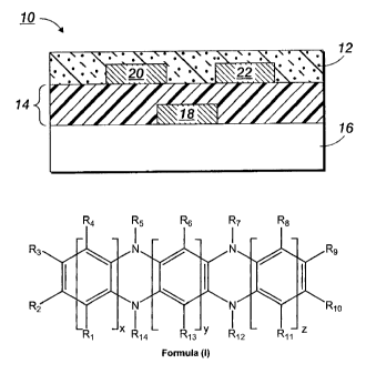
[0086] FIG. 1 illustrates a first organic thin film transistor (OTFT)
embodiment
or configuration. The OTFT 10 comprises a substrate 20 in contact with the
gate
electrode 30 and a dielectric layer 40. Although here the gate electrode 30 is
depicted within the substrate 20, this is not required. However, of some
importance is that the dielectric layer 40 separates the gate electrode 30
from the
source electrode 50, drain electrode 60, and the semiconducting layer 70. The
source electrode 50 contacts the semiconducting layer 70. The drain electrode
60 also contacts the semiconducting layer 70. The semiconducting layer 70 runs
over and between the source and drain electrodes 50 and 60. An optional
interfacial layer 80 is located between dielectric layer 40 and semiconducting
layer 70.
[0087] FIG. 2 illustrates a second OTFT embodiment or configuration. The
OTFT 10 comprises a substrate 20 in contact with the gate electrode 30 and a
dielectric layer 40. The semiconducting layer 70 is placed over or on top of
the
dielectric layer 40 and separates it from the source and drain electrodes 50
and
60. Optional interfacial layer 80 is located between dielectric layer 40 and
semiconducting layer 70.
[0088] FIG. 3 illustrates a third OTFT embodiment or configuration. The
OTFT 10 comprises a substrate 20 which also acts as the gate electrode and is
in contact with a dielectric layer 40. The semiconducting layer 70 is placed
over
or on top of the dielectric layer 40 and separates it from the source and
drain
electrodes 50 and 60. Optional interfacial layer 80 is located between
dielectric
layer 40 and semiconducting layer 70.
-19-
CA 02762460 2011-12-16
[0089] FIG. 4 illustrates a fourth OTFT embodiment or configuration. The
OTFT 10 comprises a substrate 20 in contact with the source electrode 50,
drain
electrode 60, and the semiconducting layer 70. The semiconducting layer 70
runs over and between the source and drain electrodes 50 and 60. The
dielectric
layer 40 is on top of the semiconducting layer 70. The gate electrode 30 is on
top
of the dielectric layer 40 and does not contact the semiconducting layer 70.
Optional interfacial layer 80 is located between dielectric layer 40 and
semiconducting layer 70.
[0090] The semiconducting layer formed using the semiconductor composition
can be from about 5 nanometers to about 1000 nanometers deep, including from
about 20 to about 100 nanometers in depth. In certain configurations, such as
the configurations shown in FIGS. 1 and 4, the semiconducting layer completely
covers the source and drain electrodes.
[0091] A thin film transistor generally includes a substrate, an optional gate
electrode, source electrode, drain electrode, and a dielectric layer in
addition to
the semiconducting layer.
[0092] The substrate may be composed of materials including but not limited
to silicon, glass plate, plastic film or sheet. For structurally flexible
devices, plastic
substrate, such as for example polyester, polycarbonate, polyimide sheets and
the like may be preferred. The thickness of the substrate may be from about 10
micrometers to over 10 millimeters with an exemplary thickness being from
about
50 to about 100 micrometers, especially for a flexible plastic substrate and
from
about 0.5 to about 10 millimeters for a rigid substrate such as glass or
silicon.
[0093] The dielectric layer generally can be an inorganic material film, an
organic polymer film, or an organic-inorganic composite film. Examples of
inorganic materials suitable as the dielectric layer include silicon oxide,
silicon
nitride, aluminum oxide, barium titanate, barium zirconium titanate and the
like.
Examples of suitable organic polymers include polyesters, polycarbonates,
poly(vinyl phenol), polyimides, polystyrene, polymethacrylates, polyacrylates,
epoxy resin and the like. The thickness of the dielectric layer depends on the
dielectric constant of the material used and can be, for example, from about
10
nanometers to about 500 nanometers. The dielectric layer may have a
conductivity that is, for example, less than about 10"12 Siemens per
centimeter
-20-
CA 02762460 2011-12-16
(S/cm). The dielectric layer is formed using conventional processes known in
the
art, including those processes described in forming the gate electrode.
[0094] In the present disclosure, the dielectric layer may be surface modified
with a surface modifier. Exemplary surface modifiers include
hexamethyldisilazane (HMDS) and octyltrichlorosilane (OTS-8). The
semiconducting layer can be directly contacted with this modified dielectric
layer
surface. The contact may be complete or partial. This surface modification can
also be considered as forming an interfacial layer between the dielectric
layer and
the semiconducting layer.
[0095] The gate electrode is composed of an electrically conductive material.
It can be a thin metal film, a conducting polymer film, a conducting film made
from conducting ink or paste, or the substrate itself, for example heavily
doped
silicon. Examples of gate electrode materials include but are not restricted
to
aluminum, gold, silver, chromium, indium tin oxide, conductive polymers such
as
polystyrene sulfonate-doped poly(3,4-ethylenedioxythiophene) (PSS-PEDOT),
and conducting ink/paste comprised of carbon black/graphite. The gate
electrode
can be prepared by vacuum evaporation, sputtering of metals or conductive
metal oxides, conventional lithography and etching, chemical vapor deposition,
spin coating, casting or printing, or other deposition processes. The
thickness of
the gate electrode ranges for example from about 10 to about 200 nanometers
for metal films and from about 1 to about 10 micrometers for conductive
polymers. Typical materials suitable for use as source and drain electrodes
include those of the gate electrode materials such as aluminum, gold, silver,
chromium, zinc, indium, conductive metal oxides such as zinc-gallium oxide,
indium tin oxide, indium-antimony oxide, conducting polymers and conducting
inks. Typical thicknesses of source and drain electrodes are, for example,
from
about 40 nanometers to about 1 micrometer, including more specific thicknesses
of from about 100 to about 400 nanometers.
[0096] Typical materials suitable for use as source and drain electrodes
include those of the gate electrode materials such as gold, silver, nickel,
aluminum, platinum, conducting polymers, and conducting inks. In specific
embodiments, the electrode materials provide low contact resistance to the
semiconductor. Typical thicknesses are about, for example, from about 40
nanometers to about 1 micrometer with a more specific thickness being about
-21-
CA 02762460 2011-12-16
100 to about 400 nanometers. The OTFT devices of the present disclosure
contain a semiconductor channel. The semiconductor channel width may be, for
example, from about 5 micrometers to about 5 millimeters with a specific
channel
width being about 100 micrometers to about 1 millimeter. The semiconductor
channel length may be, for example, from about 1 micrometer to about 1
millimeter with a more specific channel length being from about 5 micrometers
to
about 100 micrometers.
[0097] The source electrode is grounded and a bias voltage of, for example,
about 0 volt to about 80 volts is applied to the drain electrode to collect
the
charge carriers transported across the semiconductor channel when a voltage
of,
for example, about +10 volts to about -80 volts is applied to the gate
electrode.
The electrodes may be formed or deposited using conventional processes known
in the art.
[0098] If desired, a barrier layer may also be deposited on top of the TFT to
protect it from environmental conditions, such as light, oxygen and moisture,
etc.
which can degrade its electrical properties. Such barrier layers are known in
the
art and may simply consist of polymers.
[0099] The various components of the OTFT may be deposited upon the
substrate in any order. Generally, however, the gate electrode and the
semiconducting layer should both be in contact with the gate dielectric layer.
In
addition, the source and drain electrodes should both be in contact with the
semiconducting layer. The phrase "in any order" includes sequential and
simultaneous formation. For example, the source electrode and the drain
electrode can be formed simultaneously or sequentially. The term "on" or
"upon"
the substrate refers to the various layers and components with reference to
the
substrate as being the bottom or support for the layers and components which
are on top of it. In other words, all of the components are on the substrate,
even
though they do not all directly contact the substrate. For example, both the
dielectric layer and the semiconductor layer are on the substrate, even though
one layer is closer to the substrate than the other layer. The resulting TFT
has
good mobility and good current on/off ratio.
[0100] The following examples illustrate compounds and electronic devices
made according to the methods of the present disclosure. The examples are
merely illustrative and are not intended to limit the present disclosure with
regard
-22-
CA 02762460 2011-12-16
to the materials, conditions, or process parameters set forth therein. All
parts are
percentages by weight unless otherwise indicated.
EXAMPLES
EXAMPLE I
[0101] 5,7,12,14-tetrahydrotetraazapentacene, corresponding to that of
Formula (1), was prepared.
[0102] 1,2-Phenylene diamine (8.37 grams, 77 mmol, 2.2 equivalents) and
1,2,4,5-tetrahydroxybenzene (5.0 grams, 35.2 mmol, 1 equivalent) were ground
together using a mortar and pestle and transferred to an amber jar and purged
thoroughly with argon. The jar was sealed and placed in a 180 C oven for 4
hours. The crude product was purified by train vacuum sublimation (sample
furnace temperature 360 C) to afford the product as a dark purple (black)
solid
with a metallic green shine.
[0103] The product had a sublimation temperature of approximately 350 C.
The product was sparingly soluble in DMSO, DMF, NMP, and THF; and had low
to no solubility in alcohols and hydrocarbons. Solvatochromic behavior was
also
observed; in DMSO a bright fluorescent red/pink color was observed. The
product could also be protonated with strong acids (HCI, H2SO4) to form a deep
red-colored solution. Alternatively, the product could be deprotonated with
strong
bases (NaOH) to form a deep blue-colored solution.
[0104] In DSC, no thermal event was observed up to 350 C.
[0105] In TGA, there was less than 1% loss at 300 C; 4% loss at 450 C; and
major product loss began around 550 C.
[0106] A molecular weight of 286.1218 Da was calculated. Using MALDI-TOF
mass spectrometry, a molecular weight of 285.8100 Da was observed.
EXAMPLE 2
[0107] TH-TAP can also be prepared as described below. 1,2-Phenylene
diamine (799 milligrams, 7.39 mmol, 2.1 eq) and pyrocatechol (500 mg, 3.52
mmol, 1 eq) were ground together using a mortar and pestle and transferred to
an amber jar and purged thoroughly with Argon. The amber jar was clamped by
the lid and heated in an oven at 180 C for 4 hours. A green residue was
present
-23-
CA 02762460 2011-12-16
on the side of the vial with a dark (black) residue at the bottom. The sample
was
purified by train vacuum sublimation with a first zone (sample) at 360 C and a
second zone at 340 C to afford a metallic green solid.
EXAMPLE 3
[0108] 2,3,9, 1 0-tetramethyl-5,7,12,14-tetrahydrotetraazapentacene was
prepared. This compound is illustrated as Formula (2) below:
H3C N N CH3
I a I
H3C H H CH3
Formula (2)
[0109] 1,2,4,5-tetrahydroxybenzene (2.0 grams, 14.1 mmol) and 4,5-
dimethyl-1,2-phenylenediamine (3.83 grams, 28.2 mmol) were ground together
with a mortar and pestle, and placed in a tightly sealed vial under an argon
atmosphere. The vial was heated in a 180 C oven for 4 hours, then opened to
air
and allowed to cool. The resulting material was washed with acetone several
times, filtered, and dried.
[0110] A portion (2 grams) of the isolated sample was slowly added to
trifluoroacetic acid (175 mL) over a 30 minute period and allowed to dissolve
for
45 minutes. The resulting solution was filtered to remove insoluble
impurities.
The filtrate (a dark blue mixture) was added slowly to ice-cold deionized
water
(700 mL). The resulting precipitate was collected by filtration, reslurried in
deioized water, filtered, and dried in a vacuum oven at 50 C to afford the
product
as a black-purple solid (1.52 grams).
EXAMPLE 4
[0111] 9,10-dimethyl-5,7,12,14-tetrahydroazapentacene was prepared. This
compound is illustrated as Formula (3) below:
-24-
CA 02762460 2011-12-16
H H
N oxxxz::
H H
Formula (3).
[0112] 1,2-Phenylene diamine (761 mg, 7.04 mmol, 1 eq) and 1,2,4,5-
tetrahydroxybenzene (1.00 grams, 7.04 mmol, 1 eq) were ground together using
a mortar and pestle and transferred to an amber jar and purged thoroughly with
Ar. The jar was sealed and placed in a 180 C oven for 3 hours. The jar was
cooled to room temperature and the material was blended with 4,5-
dimethylphenylenediamine (958 mg, 7.04 mmol, 1 eq) in a mortar and pestle.
The jar was purged with Argon, sealed, and placed in a 180 C oven for 3
hours.
The sample was removed from the oven and cooled to room temperature. The
sample was a mass of black (shimmery green) solid. The sample weighed 2.03
grams indicating a yield of 92%.
-25-
CA 02762460 2011-12-16
EXAMPLE 5
[0113] A compound of Formula (4) was prepared:
I H3 I H3
o~c~c
CH3 CH3
Formula (4).
[0114] 1,2,4,5-tetrahydroxybenzene (158 mg, 1.11 mmol, 1.0 eq.) was ground
to a fine powder using a mortar and pestle and then added to a glass vial
containing N,N'-dimethyl-o-phenylenediamine (303 mg, 2.22 mmol, 2.0 eq.). The
vial was flushed thoroughly with argon, sealed, and then heated slightly under
a
flame gun to make a homogeneous solid. The reaction was heated to 180 C for
4 hours to afford a brown solid.
EXAMPLE 6
[0115] A compound of Formula (5) was prepared:
~ N N
\ I
NI N
Formula (5).
[0116] To a vial containing argon-degassed acetic acid (2.5 mL) was added
N,N'-diphenyl-o-phenylenediamine (131 mg, 0.50 mmol, 2.0 eq.) followed by
1,2,4,5-tetrahydroxybenzene (35.6 mg, 0.25 mmol, 1.0 eq.). The result was a
pink suspension. The reaction was heated to reflux for 5 days under an argon
-26-
CA 02762460 2011-12-16
atmosphere. All solid initially dissolved upon heating to form a clear
solution.
The solution gradually darkened over the course of 5 days, and a dark
precipitate
formed. The reaction was completely black after 5 days.
[0117] The compounds and devices of the present disclosure have been
described with reference to exemplary embodiments. Obviously, modifications
and alterations will occur to others upon reading and understanding the
preceding detailed description. It is intended that the present disclosure be
construed as including all such modifications and alterations insofar as they
come
within the scope of the appended claims or the equivalents thereof.
-27-