Note: Descriptions are shown in the official language in which they were submitted.
CA 02762475 2011-12-15
245278
SWITCHING CIRCUITS AND METHODS OF TESTING
The present invention relates to switching circuits and methods of testing
thereof.
Often, switching circuits include several switching devices connected in
parallel with one
another whereby the current capacity of the switching circuit is the sum of
the capacities
of each switching device. This is particularly useful for applications in
which the power
required by the load exceeds the capacity of a single switching device. One
example of
such switching circuits is found in aircraft power distribution systems,
wherein for
example 8 solid-state switching devices may be provided in parallel.
Generally, the
switching devices can fail open or closed. Each switching device has a driver
which can
be the cause of the failure. If one or more of the switching devices fails
open the others
can act as backup switches, but potentially may be subjected to current
overload. If one or
more of the switching devices fails closed, it would not be possible to switch
off the
switching circuit and it would be readily apparent that such a failure had
occurred. If
failed open, the failure may be undetectable. Solid-state switching devices
are tested
thoroughly at the manufacturing stage, but it is desirable to be able to test
them in service
to ensure that they remain fully functional. This is also known as a built-in-
test (BIT).
The present invention provides a switching circuit for connection to a load
and to a
voltage source, comprising one or more switching devices for switching on and
off power
to the load, a pulldown device for shorting out the load thereby isolating it
from the
voltage source and a controller operable while the load is shorted to activate
at least one
of the switching devices at a time, wherein a current passes through the or
each activated
switching device and is measurable to test whether the or each activated
switching device
is operating correctly.
1
CA 02762475 2011-12-15
245278
Advantageously, the pulldown device allows the switching devices to be tested
without
the load, so that the test can be carried out before or after installation of
the switching
circuit.
Further, the present invention provides a method of testing a switching
circuit that
connects a load to a voltage source, the switching circuit including one or
more switching
devices, the method comprising shorting out the load by activating a pulldown
device,
activating one or more of the switching devices, measuring the current through
the or
each activated switching device and determining from the measured current
signal
whether the activated switching devices is/are operating correctly.
Embodiments of the present invention will now be described, by way of example
only,
with reference to the accompanying drawings, in which:
Figure 1 shows schematically a circuit including a switching circuit
exemplifying the
present invention; and
Figure 2 is a graph of current against time during a test procedure carried
out on the
circuit of Figure 1.
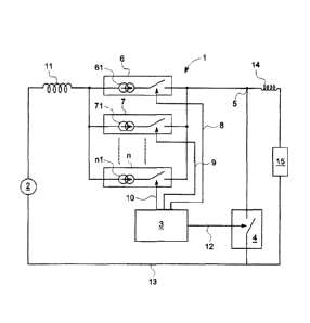
Figure 1 illustrates an example of a circuit comprising a switching circuit 1
connected to
a voltage source 2. The circuit has an output 5 which is connected to a load
15. The
circuit may, for example, be provided on an aircraft such that the voltage
source 2 may be
provided by an engine generator and the load 15 may be a component on the
aircraft,
such as to actuate a landing gear flap or the under carriage or a component
within the
aircraft such as instrumentation or in-flight entertainment. The switching
circuit 1 may
comprise an individual switching device 6, or a plurality of switching devices
6, 7, ..., n.
The switching devices are connected in parallel. The switching devices may
each
comprise any suitable solid-state switching device such as a field effect
transistor. The
switching circuit 1 is used to connect the power source 2 to the load 15. The
voltage
source 2 and its associated cabling or wiring will have an inherent inductance
11.
2
CA 02762475 2011-12-15
245278
Likewise, the load and its associated cabling and wiring will have an inherent
inductance
14.
The switching circuit further includes a controller 3 which is connected to
each of the
switching devices 6, 7, ..., n via respective control lines 8,9,10. The
controller 3 is also
connected to a pulldown device 4 via a pulldown control line 12. The pulldown
device 4
is further connected to the load output 5 and the power return line 13. When
the
pulldown 4 is closed it shuts off the load from the switching circuit, and
diverts current
through the pulldown 4. The pulldown device, also referred to as a pulldown
circuit or
simply a pulldown, can include any appropriate switch, including electronic,
electromechanical and mechanical switches.
The switching circuit 1 may comprise a solid-state power controller (SSPC),
which may
comprise one or a plurality of connected semiconductor devices. If it
comprises a
plurality of parallel connected semiconductor devices, each device may be
switched on
and off sequentially so that each of the plurality of devices may be tested
individually.
Other test sequences can be envisaged, such as activating more than one
switching device
at once. Individual activation of the switching devices allows fault isolation
to an
individual switch. The testing sequence can be carried out at any convenient
time, such as
in between flights. The testing sequence could also be carried out in-flight
during times
when the load 15 is not required.
Each of the switching devices 6, 7, ..., n includes a respective current
limiter 61, 71,...,
n1. The current limiters restrict the current passing through the switching
devices to on
the order of five to ten times the normal maximum operating current to avoid
damage to
the switching devices. Alternatively, a single current limiter for all of the
switching
devices could be provided. In a further alternative, a hard current trip could
be provided
to turn off the switching devices when the trip limit is exceeded.
The pulldown circuit is activated whenever any of the switching devices are
activated for
the BIT testing routine. Each switching device and its drive circuitry may be
fully tested
3
CA 02762475 2011-12-15
245278
by using the controller 3 to activate one device at a time while
simultaneously checking
that the current flowing through it and through the pulldown device is within
the correct
limits. The current measuring circuitry is not shown in Figure 1. In one
particular
embodiment, the minimum time for which each switching device is activated is
chosen to
be at least the time required for the current to become relatively constant to
allow
consistent measurement of this current to the accuracy required by the BIT
system. The
time for which each switching device is activated is generally dependent on
the maximum
total inductance 11 in the input power source cable. However, the system can
be operated
on shorter timescales if desired.
The pulldown device is designed so that when it sinks the current from a
single main
switching device during the BIT test, the voltage developed at the output 5 to
the load is
negligible compared to the normal output voltage when the system is on. This
ensures
that the load is not subjected to significant voltage when the system is
supposed to be off.
This is achieved by using a pulldown device 4 that has a lower impedance than
each
switching device, preferably much lower. In practice, when the current
limiters 61, 71,
..., n1 are in operation, the switching devices 6, 7, ..., n have a higher
effective
impedance than the pulldown device 1. During normal system operation, the
controller 3
which activates the switching devices 6, 7, ..., n would generally be expected
to turn all
of the switching devices on and off simultaneously.
Embodiments of the invention apply not only to DC systems but also AC systems.
In this
case the voltage source 2 would be an alternating voltage. The switching
devices would
be AC switches (optionally with AC current limiters) and the pulldown circuit
would be
capable of sinking AC currents. In a DC embodiment, the pulldown device
comprises a
field effect transistor (FET) or a bipolar transistor, or an insulated gate
bipolar transistor
for example. Other types of switching device can be used. In an AC embodiment,
the
pulldown device may comprise a triac or a solid state relay for example.
Figure 2 illustrates the output current through a switching device when a test
procedure is
performed. Only one peak is shown, but in an exemplary embodiment eight
switching
4
CA 02762475 2011-12-15
245278
devices are provided so the test would result in a total input current from
the voltage
source 2 which shows 8 sequential pulses like the single one shown in Fig. 2.
The correct
operation of each switching device 6, 7, ..., n may be determined by checking
the
amplitude of each individual current pulse is within the correct limits.
The test procedure begins by shorting out the load by activating the pulldown
device 4.
The pulldown device will generally remain on for the duration of the BIT test.
The first
switching device 6 is closed at about 250 s in the example shown, and the
current
through the switching device 6 quickly rises to that provided by the source 2,
in this
example approximately 100 Amps. The first switching device 6 is then opened
and a
short time later, the second switching device 7 is closed and the current
through the
second switching device 7 is measured. This procedure is repeated in sequence
until all
of the switching devices have been tested. Differences in the current profiles
to the ones
shown in Figure 2 may indicate a fault with the corresponding switching
device.
Advantageously, embodiments of the invention allow individual assessment of
the
operation of the switching devices. A simple BIT test which just checks the
overall solid
state power controller operation would not normally be able to detect a faulty
device
which was stuck in the open circuit state. A technical advantage of this
invention is that
not only does it detect single device failures but also can check the current
limiting
performance of each device individually. The invention can therefore provide
complete
BIT coverage during in-service operation.
In an alternative embodiment the switching devices do not have current limit
control. In
this case the inductance of the power source 2 and cable inductance 11 can be
relied on in
combination with a fast current trip circuit to prevent the current rising to
dangerous
levels during the test pulse. In other words, the controller 3 in this
embodiment would
operate to activate the sequence of opening and closing the switching devices
quickly
enough to avoid current overload.