Note: Descriptions are shown in the official language in which they were submitted.
CA 02762947 2011-11-21
WO 2010/139562 PCT/EP2010/056958
1
TV signal distribution filter having planar inductors
Technical field
The present invention relates generally to filters in programmable
electronic TV signal distribution devices that selectively process TV
signals received from antenna or cable and deliver a processed signal
which is distributed over a plurality of TV sets.
Background art
In TV reception, a selective processing of the received signals is
required. The desired signals with known frequencies have to be passed,
while the others have to be suppressed. This has been realised by the
electronic circuits called filters, in most cases band-pass filters.
An analogue circuit solution of the band-pass filter consists at least
of one inductor and one capacitor (frequency tuning circuit), more often
different combinations of more inductors and capacitors. The simplest
filter of the first generation had both a fixed centre frequency and a fixed
bandwidth. A corresponding circuit has also all fixed inductors and
capacitors within its structure. Such a solution was very cheap but did not
allow simple retuning if needed.
The second filter generation brought circuits with tuneable band-
pass centre frequency while the bandwidth was still constant (e.g.
GB2272341). Such a solution was sufficient for the late analogue TV
transmission characterized by a fixed bandwidth of the TV channels. The
filter circuit can be retuned generally by the change of either inductor or
CA 02762947 2011-11-21
WO 2010/139562 PCT/EP2010/056958
2
capacitor value. The most suitable components for retuning are varicap
diodes which can be used as a voltage-controlled capacitor if they are
operated reverse-biased. It is why the second filter generation consisted
not only of fixed inductors and capacitors but also of varicap diodes.
Varicap diodes were employed here as the element which enabled
electronically (by the usage of an accompanying digital control part)
retuning of the filter.
The newest digital transmission concept brought a requirement to
retune in the filters both the band-pass centre frequency and bandwidth.
The reason is that the TV channels are broadcasted in groups - clusters
of analogue and digital channels. The third filter generation solves this by
a bigger complexity of the filter circuits. The varicap diodes are used here
not only to retune a centre frequency of the band-pass filters but also to
change a coupling between the tuning circuits. An example of such device
can be found in the Unitron N.V. product range and has been described in
EP1794883.
A crucial parameter in all the three generations of the filters is the
selectivity. It defines how much the practical filter differs from the ideal
one which has a completely flat pass band and a zero roll-off (all
frequencies outside the desired frequency range are completely
suppressed). To achieve the best selectivity, the filter circuits have been
only equipped with aerial coils which have the highest quality factor for
the practical usage.
A disadvantage of using aerial coils is that the shape of all used
coils of the frequency tuning circuits must be set. Further, between some
of the filter coils one even has to set very accurately the distance (filter
coupling factor). As a result, this is typically performed by manually
shaping the coils to reach a target characteristic on the measurement
equipment (network analyser), which requires highly skilled people.
Optionally a programmed robot can be used to do the shaping
CA 02762947 2011-11-21
WO 2010/139562 PCT/EP2010/056958
3
automatically. In both cases, the process is however time consuming and
needs expensive machinery. So even though technology can be used to
reach a high quality factor of the coils in the filters, the fabrication
process
is very complex and leads to a high cost price of the product.
Furthermore, increasing the production capacity is not easy since one has
to find highly skilled person or invest in expensive machinery.
Disclosure of the invention
It is an aim of the present invention to provide a TV signal
distribution filter device which can be manufactured at a reduced cost
while still obtaining a high quality factor.
This aim is achieved according to the invention with a TV signal
distribution filter device showing the technical characteristics of the first
claim.
Thereto, the present invention provides a TV signal distribution
filter device having at least one tuneable band-pass filter circuit, wherein
the inductors are provided as planar inductors instead of the aerial coils
used in the prior art. The planar inductors are mechanically fixed and
embedded in a dielectric environment. The advantage of planar inductors
is that they have a fixed and easily reproducible morphology, so the filter
production flow can be made much faster and economical. Especially
since there is no longer a need for a manual tuning step.
Another advantage of the use of planar inductors is that they can
be easily integrated in a Surface Mount Technology (SMT) production
process.
Another advantage is that there is no longer a need to use
separated varicap diode voltages for different tuning circuits and
separated voltages for coupling varicap diodes between tuning circuits
within one filter. With the aerial coils used in the prior art there were big
tolerances on the parameters (coil shape and through hole soldering),
CA 02762947 2011-11-21
WO 2010/139562 PCT/EP2010/056958
4
whereas the planar inductors used according to the invention are highly
reproducible.
Another advantage is also that the radiation of the aerial coils is
cancelled in the filter device, which had to be carefully eliminated in the
prior art by a shielding especially in the case of multiple filters. As the
planar inductors which are used according to the invention are embedded
in a dielectric environment, the risk of parasitic feedback and signal
leakage between neighbour filters is minimised without further shielding.
In preferred embodiments of the invention, the planar inductors are
provided in a single conductive layer of the dielectric environment, which
is in this case preferably a single sided printed circuit board (PCB)
substrate. Such a low cost solution enables to integrate planar inductors
with other components of the TV signal distribution filter to a common unit,
easy to produce and at low cost.
In preferred embodiments of the invention, the planar inductors are
provided in different conductive layers of the dielectric environment, which
is in this case preferably a double-sided or multilayer PCB substrate.
Such a solution can significantly improve the selectivity of the filter.
Preferably, the first and second inductors overlap each other at least
partly (i.e. are located partly above each other seen in a direction
perpendicular to the planes of the planar inductors).
In preferred embodiments of the invention, the device comprises a
plurality of tuneable band-pass filter circuits connected in a cascade. With
two or more band-pass filtering circuits in series, a better selectivity of
the
total filtering can be achieved. Such a cascaded section can be either
provided by a simple joining of the filter circuits or can be also realised
with intermediate matching circuits or amplifiers, if necessary.
Preferably, in such a case, the planar inductors of the cascaded
tuneable filter circuits have a predetermined morphology, such that
synchronised relations exist between the tuning voltage and the
CA 02762947 2011-11-21
WO 2010/139562 PCT/EP2010/056958
respective filtering parameters in each of the cascaded tuneable filter
circuits. This means that the morphology (the design of the physical
structure) of the planar inductors of the different filter circuits in the
cascade is optimised with respect to each other, such that the relation
5 between the tuning voltage and the respective filtering parameter (e.g.
centre frequency, cut-off frequency, coupling, ...) in a first stage of the
cascade is equal to or proportional to the relation between the tuning
voltage and the same filtering parameter in a second stage of the
cascade. In this way a common voltage can be used for controlling the
varicap diodes used in tuning circuits of two or more filters in series.
Depending on the practical tolerance of the dielectric environment,
different options are possible. A first being the integration of the complete
circuitry on 1 PCB, a second being the implementation of each filter on a
separate PCB, a third being the implementation of each inductor or
combination of inductors on a separate PCB.
Brief description of the drawings
The invention will be further explained by means of the following
description and the appended figures.
Figure 1 schematically shows a prior art TV signal distribution
band-pass filter with aerial coils.
Figure 2 schematically shows a TV signal distribution band-pass
filter having planar inductors according to the present invention.
Figure 3 schematically shows an embodiment of the invention
where the planar inductors have been realised by an etched conductive
layer on a single sided PCB substrate.
Figure 4 schematically shows an embodiment of the invention
where the planar inductors have been realised by an etched conductive
layer on a double-sided PCB substrate.
CA 02762947 2011-11-21
WO 2010/139562 PCT/EP2010/056958
6
Figure 5 schematically shows a preferred embodiment of a TV
signal distribution band-pass filter according to the present invention.
Figure 6 schematically shows two tuneable filter circuits connected
in a cascade for achieving better selectivity of the total filtering. The
cascaded section has been provided here by an intermediate amplifier.
Modes for carrying out the invention
The present invention will be described with respect to particular
embodiments and with reference to certain drawings but the invention is
not limited thereto but only by the claims. The drawings described are
only schematic and are non-limiting. In the drawings, the size of some of
the elements may be exaggerated and not drawn on scale for illustrative
purposes. The dimensions and the relative dimensions do not necessarily
correspond to actual reductions to practice of the invention.
Furthermore, the terms first, second, third and the like in the
description and in the claims, are used for distinguishing between similar
elements and not necessarily for describing a sequential or chronological
order. The terms are interchangeable under appropriate circumstances
and the embodiments of the invention can operate in other sequences
than described or illustrated herein.
Moreover, the terms top, bottom, over, under and the like in the
description and the claims are used for descriptive purposes and not
necessarily for describing relative positions. The terms so used are
interchangeable under appropriate circumstances and the embodiments
of the invention described herein can operate in other orientations than
described or illustrated herein.
The term "comprising", used in the claims, should not be
interpreted as being restricted to the means listed thereafter; it does not
exclude other elements or steps. It needs to be interpreted as specifying
the presence of the stated features, integers, steps or components as
CA 02762947 2011-11-21
WO 2010/139562 PCT/EP2010/056958
7
referred to, but does not preclude the presence or addition of one or more
other features, integers, steps or components, or groups thereof. Thus,
the scope of the expression "a device comprising means A and B" should
not be limited to devices consisting only of components A and B. It means
that with respect to the present invention, the only relevant components of
the device are A and B.
Figure 1 shows a typical prior art TV signal distribution band-pass
filter with aerial coils 22, 23. It is an electronically tuned band-pass
filter
with aerial coils and varicap diodes which enable to set both band-pass
centre frequency and bandwidth by the voltages. The circuit has a signal
input 1, has a signal output 17, has pins 2 and 18 for providing a
frequency tuning voltage and has a pin 16 for providing an external
bandwidth setting voltage. The filter circuit comprises an input capacitor 3
and an output capacitor 14 for DC blocking the incoming and outgoing
signals. Also capacitors 6, 9 and 12 block DC voltages from the varicap
diodes 5, 7 and 11. The filter circuit further comprises resistors 4, 13 and
15 for the DC biasing of varicap diodes 5, 7 and 11. The filter circuit
comprises two tuning circuits; the first comprises capacitor 6, varicap
diode 5 and coil 22. The second tuning circuit comprises coil 23, varicap
diode 11 and capacitor 12. These tuning circuits are tuned by tuning
voltages entering via pins 2 and 18 to reach a required band-pass centre
frequency of the whole filter. An external voltage on the pin 16 sets a
coupling between the tuning circuits by changing the varicap diode 7
capacitance. In this way the frequency bandwidth of the filtering is
controlled.
The coils 22 and 23 in the typical prior art TV signal distribution
band-pass filter have an aerial design. As the varicap diodes have limited
minimum and maximum voltage, the fabrication process has to ensure that
the coils 22 and 23 in the filter have a shape within some mechanical
limits (determines the frequency) and also that their relative distance has
CA 02762947 2011-11-21
WO 2010/139562 PCT/EP2010/056958
8
only a small tolerance (determines the bandwidth). Such a process can
make the device very expensive.
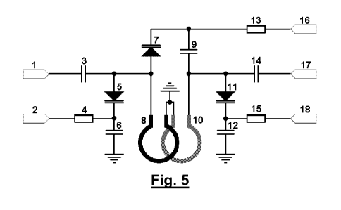
Figure 5 shows a TV signal distribution band-pass filter according
to the invention. The filter circuit has the same components as the prior
art circuit of figure 1, except for the inductors 8, 10, which are here planar
inductors, mechanically fixed and embedded in a dielectric environment.
This gives them an accurate and reproducible shape (inductance) and
cross distance (coupling). In this way the necessity of the additional
shaping/tuning of the coils during the production flow is eliminated. If
sufficient care is taken in designing the shape and distance of the
inductors and in the accuracy of the lithography process, the resulting
device can become highly reproducible.
Figures 2-4 show alternative embodiments for the planar inductors
8, 10 of a band-pass filter device according to Fig. 5. In Fig. 2, the
inductors have been defined by a lithography process in a single
conductive layer embedded in a dielectric substrate 19. As a result,
unintended radiation to other inductors is much smaller in comparison
with the aerial coils of the prior art. In this way a shielding system in the
device can be reduced or even eliminated.
In the embodiment of Fig. 3, the planar inductors 8 and 10 have
been manufactured by etching a conductive layer on a single sided PCB
substrate surface 20. Such a way of the fabrication is fully compatible with
the other assembling technology and can make the production very
economical.
The inductors 8 and 10 can also be placed in different conductive
layers of a double-sided or even a multilayer PCB substrate 21, as shown
in the Fig. 4. Such a solution has the advantage of a potential overlapping
of the coils if needed comparing to the above mentioned single sided PCB
solution. Such a morphology enables to increase a coupling factor and
can significantly improve a selectivity of the filter as well. Overlapping the
CA 02762947 2011-11-21
WO 2010/139562 PCT/EP2010/056958
9
coils also makes the filter less sensitive for the external interferences.
Last but not least, the overlapped morphology of the coils consumes less
space. Extra conductive layers on the substrate of multilayer PCBs can be
used for additional shielding which can decrease the required coupling
between coils of the same filter and unwanted radiation to the
neighbourhood, and can also decrease an external interference
sensitivity.
It is also possible to use more than one filter circuit in the signal
path if the filter selectivity is insufficient. To do so, it could be needed
to
use an intermediate impedance matching and/or signal level amplification
circuits. Figure 6 shows an example of such a cascade connection of two
tuneable filter circuits. They are both electronically tuned band-pass filters
with planar inductors 8, 10, 8', 10' and varicap diodes 5, 7, 11, 5', 7', 11'
and associated voltage nodes 2, 16, 18, 2', 16', 18' which enable to set
both band-pass centre frequency and bandwidth in both stages of the
cascade. The circuit has a signal input 1 and has a signal output 17'. The
amplifier 19 in between the tuneable filter circuits compensates a signal
loss caused by the filtering and can even bring a positive gain of the total
circuit. The functionality of the other components of the first stage is the
same as has been described by means of figure 1. The like components
of the second stage having the single quoted reference numbers also
have an analogical purpose and therefore need no further description
here.
Especially in the case of using more filters in series it can be very
useful to ensure synchronised controlling of as much as possible
frequency voltages and as much as possible bandwidth voltages. This can
be achieved by the careful design of morphology of all planar inductors
and distances (overlapping) between them. In the best case, for a band-
pass filter, the full cascade of the filters can be fully controlled by only
two
voltages, which according to the embodiment of figure 6 would mean that
CA 02762947 2011-11-21
WO 2010/139562 PCT/EP2010/056958
the voltage nodes 2, 2', 18 and 18' receive a first voltage and the voltage
nodes 16, 16' receive a second voltage. The first voltage controls the
centre frequency and the second voltage controls the bandwidth of the
frequency filtering.
5 In the figures, the planar inductors are shown as circular single
winding elements. In alternative embodiments, the planar inductors can
also be rectangular, oval or other shapes and can have multiple windings,
possibly also on different conductor planes of the dielectric environment.
In the figures and in the description above, varicap diodes have
10 been used as the tuneable capacitive components which are controlled by
the tuning voltages for setting the respective filtering parameter (e.g.
centre frequency or bandwidth). In alternative embodiments, other
tuneable capacitive components can be used as well according to the
invention, such as for example voltage controlled switched capacitor
banks.
The dielectric environment can be composed of a single dielectric
material or different dielectric materials. For example, in the embodiment
shown in figure 2, the dielectric material above the inductors can be a
different material than that below the coils. Alternatively, each inductor
can be embedded in a different dielectric material. Air can form one of the
materials of the dielectric environment, like in the embodiments shown in
figures 3 and 4.