Note: Descriptions are shown in the official language in which they were submitted.
CA 02763271 2012-01-06
DIMENSIONALLY STABLE WHITE BOARD
FIELD OF THE INVENTION
Embodiments of the present invention relate to an interactive writing surface
and,
preferably, a multipurpose writing and projection surface having a
dimensionally
stable construction.
BACKGROUND OF THE INVENTION
Whiteboards, also commonly referred to as dry erase boards or erasable marker
boards, have previously been fabricated from a dry erase surface mounted onto
a rigid substrate, such as a laminate or polycarbonate. Originally used only
as
writing surfaces for erasable markers or pens, whiteboards have since been
used
also as projection screens. For example, in U.S. 5,361,164 and U.S.
2005/0112324, Rosenbaum et al. describe a dual dry erase outer surface and
micro-roughened inner surface. The dry erase outer surface prevents inks from
being trapped in the whiteboard writing surface, while the micro-roughened
inner
surface reduces gloss to make the writing surface more suitable for use as a
projection surface simultaneously.
Another feature added to some whiteboard surfaces, often the dry erase
surface,
is contact sensitivity to convert the whiteboard into an interactive device.
For
example, by detecting pressure applied to the dry erase surface, the
whiteboard
can be converted into an input device for a computer system. One approach to
providing touch sensitivity is described in U.S. 2008/0083602 by Auger et al.
In
their design, a first conductive layer is disposed on a support substrate and
an
insulating spacer is mounted generally about the periphery of the substrate. A
second, pre-tensioned conductive layer overlies the first conductive layer
under
sufficient tension to form and maintain an air gap therebetween in the absence
of
applied pressure. However, when sufficient pressure is applied, the two
CA 02763271 2012-01-06
2
conductive layers are brought into contact. Closure of an electrical circuit
through
the contact point can then be detected to register touch.
SUMMARY OF THE INVENTION
In known white boards, the outer conductive layer may be mounted to an
adjustable frame. Over time, the outer conductive layer may sag due to changes
in the resilient characteristics of the outer conductive layer, variations in
temperature and the like. If the outer conductive layer sags too much, then it
may
contact the inner conductive layer, thereby producing an unintended signal.
Further, even if the outer conductive layer maintains its spacing from the
inner
conductive layer, a reduction in the tension of the outer conductive layer
could
cause the white board to be too touch sensitive resulting in unintentional
signals
being produced. The adjustable frame is provided with a tensioning mechanism
such that the outer conductive layer may be re-tensioned to remove any sag and
to maintain a desired spacing or air gap between the opposed inner and outer
conductive layers.
In accordance with the described embodiments, there is provided a whiteboard
having a simplified construction in which the provision of a variably
resistive
material between conductive layers eases requirements on any tensioning
mechanism used to maintain the outer conductive layer at a pre-specified
tension. In some cases, the air gap can be eliminated altogether along with
the
tensioning mechanism used to form and maintain the air gap. In other cases, an
air gap can be formed even with the resistive material provided, but less
tension
is required and/or no tensioning mechanism is required, resulting in a simpler
whiteboard construction and a lighter, more reliable and, potentially, thinner
whiteboard.
According to one broad aspect, there is provided a dry erase whiteboard with a
backing substrate having a surface, and an inner conductive layer and an outer
CA 02763271 2012-01-06
3
conductive layer supported by the surface of the substrate. A resistive layer
is
positioned between the inner conductive layer and the outer conductive layer.
To
provide progressive touch capability, the resistive layer has an electrical
resistivity that varies in response to mechanical deformation and/or
mechanical
stress, such as application of pressure, to provide a variable effective
resistance
between the inner and outer conductive layers. The resistive layer is secured
to
one or both of the inner and outer conductive layers.
A fixed frame (e.g., a frame having a plurality of frame members that are
immovably positioned on the substrate and/or, optionally, connected together)
can be mounted to the backing substrate, with the outer conductive layer
immovably attached to the fixed frame in a spaced apart relation to the inner
conductive layer and, optionally, defining an air gap therebetween. The outer
conductive layer may be provided on a flexible substrate wherein the substrate
is
affixed to the frame. The substrate may be pre-tensioned or tensioned when
applied to the frame, thereby providing a suitable surface for image
projection
and/or writing, such that the outer conductive layer is mounted tautly to the
frame.
Alternately, any tensioning assembly known in the art may be provided as part
of
the frame and the outer conductive layer to maintain the outer conductive
layer in
a tensioned state, whether or not the outer conductive layer is pre-tensioned.
Accordingly, the substrate may optionally be applied to the frame and the
frame
then adjusted to tension the substrate.
To provide a substantially air-free environment between the inner conductive
layer and the outer conductive layer, the resistive layer may be secured to
corresponding surfaces of one or both of the inner and outer conductive
layers,
such as being applied to one or both thereof, such as by screen printing the
resistive layer thereon, or by means of an adhesive in whole or in part.
Alternately, the resistive layer may be positioned adjacent or in a touching
relationship with the inner and outer conductive layers.
CA 02763271 2012-01-06
4
Preferably the inner and outer conductive layers may be formed into multiple
planar segments in close proximity to and electrically insulated from adjacent
planar segments. The planar segments in the inner and outer conductive layers
respectively are preferably positioned opposite one another (i.e., facing one
another) with the planar segments of the inner and outer conductive layers
forming, e.g., a spaced grid of squares, rectangles, diamonds or any other
suitable quadrilateral or geometric shapes. With each planar segment
independently addressed, local variation in the effective resistance between
the
inner and outer conductive layers is detectable on a per segment basis. This
enables multi-touch capability for the whiteboard in which multiple concurrent
touches are detectable.
According to another broad aspect, there is provided a method of assembling a
dry erase whiteboard in which inner and outer conductive layers are provided
and a resistive layer, formed from a material having an electrical resistivity
that
varies in response to mechanical deformation, is provided between the inner
and
outer conductive layers and is preferably applied to at least one of the inner
conductive layer and the outer conductive layer. The inner conductive layer
may
then be mounted on a surface of the backing substrate, and the outer
conductive
layer may be secured in close proximity to the first conductive layer (e.g.,
by
being mounted to a frame or mounted to the resistive layer) to provide an
effective resistance between the inner and outer conductive layers that varies
with the mechanical deformation of the resistive layer.
The resistive layer may be deposited (e.g., screen-printed) onto one of the
inner
and outer conductive layers, or it may be adhered to the other conductive
layer to
provide a substantially air free environment between the inner and outer
conductive layers. The conductive layers can also each be deposited (e.g.,
screen printed, roll-coated, blade-coated, gravure-coated, slot and die
coated)
onto corresponding flexible layers.
CA 02763271 2012-01-06
BRIEF DESCRIPTION OF THE DRAWINGS
For a better understanding of the present invention, and to show more clearly
how it may be carried into effect, reference will now be made, by way of
example,
to the accompanying drawings, which show at least one preferred embodiment of
5 the invention, and in which:
Figure 1A is cross section of a writing and projection surface according to
one
embodiment of the invention;
Figure 1B is cross section of a writing and projection surface according to
another embodiment of the invention;
Figure 1C is cross section of a writing and projection surface according to a
further embodiment of the invention;
Figure 2 is an enlarged portion of the center section of Figure 1A;
Figure 3 is a graph showing the relationship between resistance and applied
pressure of an exemplary variably resistive layer;
Figure 4A is a perspective view of an alternative embodiment, in which planar
segments are used to provide multi-touch, pressure sensitivity;
Figure 4B is a perspective view of the embodiment of Figure 4A without a
resistive layer shown;
Figure 4C is a perspective view of a further alternative embodiment, in which
planar segments are used to provide multi-touch, pressure sensitivity;
Figure 4D is a perspective view of the embodiment of Figure 4C without a
resistive layer shown;
Figure 4E is a top plan view of the embodiment of Figure 4C; and,
Figure 5 is a schematic drawing of an interactive whiteboard system according
to
another embodiment of the invention.
CA 02763271 2012-01-06
6
DESCRIPTION OF THE PREFERRED EMBODIMENT
Pressure sensitive whiteboards formed using an air gap between two conductive
layers, such as the configuration described by Auger et al., require a
tensioning
mechanism to maintain the air gap. If the tension in the outer conductive
layer is
too little, wrinkles and other deformities can appear in the writing surface
of the
whiteboard that cause poor tactile feel and that distort any images displayed
on
the whiteboard surface. This diminishes the usefulness of the whiteboard as a
writing surface and/or a projection surface. Also, if the tension in the outer
conductive is decreased even further, the two conductive layers could
inadvertently come into contact and register a false touch.
At the same time, maintaining the outer conductive layer in its tensioned
state
exerts a force on the underlying substrate or lamination to which the
whiteboard
is mounted. Due to this applied force, the lamination must have a certain
robustness to withstand the tensile strain on the outer conductive layer.
Sometimes the force applied to the lamination due to tensioning causes the
lamination to warp or otherwise torque or bend, which may again cause the
writing surface to become wrinkled and may cause the whiteboard to become
inoperable.
In either event, a complex tensioning mechanism or assembly involving spacers
and/or tension screws to maintain the outer conductive layer at the proper
tension may be required. Such a tensioning mechanism and its associated
components has a generally high labor content and a high labor cycle time
during
assembly. Each of the potentially greater number of parts requires manual
handling. Further, the tensioning mechanism is subject to failure that may
compromise the utility of the whiteboard.
The pressure sensitivity of the writing surface is also limited to single-
touch,
binary input. Accordingly, the whiteboard either registers a "touch"
(corresponding to contact made between the two conductive layers) or a "no
touch" (corresponding to no contact made between the two conductive layers).
CA 02763271 2012-01-06
7
Different strengths or degrees of touch are not recognized. There is also no
distinct identification of multiple concurrent touches. Each of these factors
limit
the available form and number of input commands that be may be received into
the whiteboard, resulting in a less intuitive input interface.
Embodiments of the present invention provide a whiteboard formed using a
resistive layer positioned between two conductive layers. The resistive layer
is
formed from a material or materials having a resistivity that varies inversely
with
applied pressure. As will be described, inclusion of the resistive layer or
layers
permits increased dimensional stability to the whiteboard and allows for
definition
of a wider range of more versatile and more intuitive input commands.
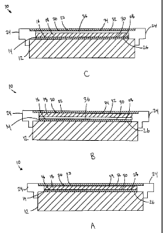
Referring now to Figure 1A, there is shown an embodiment of a whiteboard 10.
The whiteboard 10 has a backing substrate 12 on which is formed a number of
layers, including an inner flexible layer 14, an inner conductive layer 16
(solid
line), a resistive layer 18, an outer conductive layer 20 (solid line) and an
outer
flexible layer 22. The whiteboard 10 may be any size but, preferably, is a
large
scale whiteboard having a surface area of 500 square inches or more.
A peripheral frame 24 may optionally be mounted on the substrate 12 in some
embodiments. The frame may comprise a plurality of frame members that are
immovably secured together to define a frame having fixed dimensions so as to
define a fixed peripheral frame. In other embodiments, a tensioning mechanism
may be provided with the fame to define an adjustable peripheral frame.
The backing substrate 12 may be any suitable substrate known in the art for
providing backing support for the whiteboard, such as a lamination or
polycarbonate. For example, the backing substrate 12 permits the whiteboard 10
to be self-supporting or, in some cases, wall mountable. Accordingly, if the
whiteboard 10 is wall mounted, the backing substrate 12 provides sufficient
rigidity. The backing substrate 12 has an outer surface 26 on which the inner
flexible layer 14 is supported.
CA 02763271 2012-01-06
8
The inner flexible layer 14 may be secured to the outer surface 26 of the
backing
substrate 12 by any means known in the art, such as by using an adhesive
(e.g.,
a pressure sensitive adhesive). The inner flexible layer 14 may be made from
any material known in the art. Preferably, the inner flexible layer 14 is made
of a
flexible polyester or polymer material. The inner flexible layer 14 has an
outer
surface 28 on which the inner conductive layer 16 is applied. In some
embodiments, the inner flexible layer 14 may be replaced with a rigid or semi-
rigid layer, or may be omitted altogether.
The inner conductive layer 16 may be provided on the inner flexible layer 14
by
any means known in the art and may be of any composition known in the art.
Preferably the inner conductive layer 16 is deposited onto the inner flexible
layer
14, for example, as a screen-printed liquid and then cured to harden or by
roll
printing. The inner conductive layer 16 may be formed from a carbon composite
material, or another conductive material, for this purpose. An outer surface
30
(shown more particularly in Figure 2) of the inner conductive layer 16 opposes
the resistive layer 18.
As exemplified in the embodiment of Figure 1A, a pressure sensitive composite
layer may comprise the resistive layer 18 that is sandwiched between the inner
conductive layer 16 and the outer conductive layer 20 and is in touching
relationship therewith. The inner surface of the resistive layer is optionally
fixed to
the outer surface 30 of the inner conductive layer 16, and an outer surface of
the
resistive layer is optionally fixed to an inner surface 32 of the outer
conductive
layer 20. The resistive layer 18 may be screen-printed or otherwise deposited
onto either the inner conductive layer 16 or the outer conductive layer 20.
The
resistive layer 18 may then be secured immediately adjacent the other of the
conductive layers 14 and 20 on which the resistive layer 18 is not deposited
so
as to cause light contact, but without exerting undue pressure that would
change
the electrical characteristics of the resistive layer as described below.
Thereby a
CA 02763271 2012-01-06
9
substantially air free environment is formed between the inner conductive
layer
16 and the outer conductive layer 20.
The resistive layer 18 is made from a material having a resistivity (or
equivalently
a conductivity) that varies with applied pressure. For example, the
resistivity of
the resistive layer 18 may vary inversely with applied pressure, thereby to
act as
a substantial insulator when no pressure is applied, but act like an
increasingly
efficient conductive as the applied pressure increases. Accordingly, the
effective
resistance through the resistive layer 18, from the inner conductive layer 16
to
the outer conductive layer 20 is preferably large when the resistive layer 18
is in
a quiescent state and, most preferably, so is the signal produced in this
state.
As a non-limiting example, the resistive layer 18 may be a variable
resistivity ink
or liquid polymer such as is described U.S. 2010/0062148A, U.S 7301435 or
PCT Application No. W02008/135787A1 by Lussey, the disclosure of which is
incorporated herein by reference. Force sensitive resistors may also be used.
The outer conductive layer 20 may be the same or different to the inner
conductive layer 16 and may be applied to the inner surface 34 of the outer
flexible layer in the same or a different manner. For example, the outer
conductive layer 20 may be deposited or screen-printed onto the outer flexible
layer 22, which may be flexible for that purpose. Like the inner conductive
layer
16, the outer conductive layer 20 may be formed from a carbon composite
material or other conductive material.
The outer flexible layer 22 is optionally mounted to a frame, which may be a
fixed
or adjustable peripheral fame 24 in some embodiments, although this is not
necessary. Alternately, or in addition, the outer flexible layer 22, with the
outer
conductive layer 20 applied thereon, may be adhered directly to the resistive
layer 18. The outer flexible layer 22 may be a polyester or flexible polymer
layer.
Although not shown, a dry erase coating may be applied, in some cases in
combination with additional layers also not shown, to provide a dual writing
and
CA 02763271 2012-01-06
projection surface for the whiteboard 10. However, the dry erase coating is
preferably a single layer.
Referring now to Figure 1B, there is shown an alternative embodiment of the
whiteboard 10 shown in Figure 1A comprising an air gap 36. In the embodiment
5 shown in Figure 1 B, the outer conductive layer 20 is preferably attached to
the
peripheral frame 24, by way of the outer flexible layer 22, to be held in a
spaced
apart relation with respect to the inner conductive layer 16. The resistive
layer 18
does not fill the space between the inner conductive layer 16 and the outer
conductive layer 20 to form the air gap 36.
10 In some cases, the outer conductive layer 20 is tensioned to maintain the
air gap
36. For example, the outer flexible layer 22 may be mounted tautly to the
peripheral frame 24 to maintain the outer conductive layer 20 formed thereon
in
tension, although other ways of tensioning the outer conductive layer 20 are
possible. While the outer conductive layer 20 is tensioned and the air gap 36
is
maintained, it is not necessary to control the tension of the outer conductive
layer
as precisely as where the resistive layer 18 is omitted. Because the resistive
layer 18 provides a large resistivity in the quiescent state, incidental
contact
between the resistive layer 18 and the inner conductive layer 16 does not
result
in a false touch being registered. In some cases, a certain amount of slack in
the
20 outer flexible layer 22 may provide increased tactility to the whiteboard
10.
Referring now to Figure 1C, there is shown an alternative embodiment of the
whiteboard 10 shown in Figure 1B. In this alternative embodiment, the
resistive
layer 18 is in contact with the outer surface 30 of the inner conductive layer
16,
as opposed to the inner surface 32 of the outer conductive layer 32 shown in
Figure 1B.
During assembly of the whiteboard 10, the inner conductive layer 16 may be
applied to the inner flexible layer 14 and the outer conductive layer 20 may
be
applied to the outer flexible layer 22. A resistive layer 18 may then applied
to one
CA 02763271 2012-01-06
11
or both of the conductive layers. An air gap 36 may be formed as exemplified
in
Figures 1 B and 1 C as may be desired.
Referring now to Figure 2, the embodiment of the whiteboard 10 having no air
gap is shown in enlarged portion. In particular, the inner conductive layer 16
and
the outer conductive layer 20 are shown having thickness. It should be
appreciated that the dimension shown in Figure 2 may be exaggerated for
purpose of illustration.
Referring now to Figure 3, there is shown a graph 50 illustrating an exemplary
relationship between resistivity and applied pressure. The graph 50 is shown
with
arbitrary units and, it should be appreciated, can also be plotted on
different
scales. For example, the graph 50 represents the resistivity of the resistive
layer
18 (Figures 1A-1C) under mechanical deformation and/or mechanical stress,
such as caused by application of pressure or other mechanical forces.
As can be seen in Figure 3, the resistivity of the resistive layer 18 may vary
inversely with applied pressure or some other stimulus causing mechanical
deformation of the resistive layer 18. Preferably, for low applied pressures,
the
resistivity becomes very large and the resistive layer 18 behaves like an
insulator. However, for increasing applied pressure, the resistivity of the
resistive
layer 18 decreases, preferably monotonically, causing the resistive layer 18
to
behave like an increasingly efficient conductor.
Different ranges of applied pressure correspond to different ranges of the
resistivity of the resistive layer 18. Range 52 in Figure 3, which is defined
between about 6 and 8 on the y-axis, corresponds to an applied pressure of
between about 2 and 4 on the x-axis. Likewise range 54 corresponds to
progressively larger force applied to the resistive layer 18 (i.e. about 4 to
6) and
range 56 to still larger forces (i.e. about 6 to 8). These ranges may be non-
overlapping and, in a particular, case, contiguous. A linear relation is
illustrated in
Figure 3 as one exemplary relationship. However, in some embodiments, the
CA 02763271 2012-01-06
12
resistivity of the resistive layer 18 may have a convex or a concave slope
with
increasing applied pressure.
By measuring the resulting resistivity of the resistive layer 18, the amount
of the
applied pressure is measurable. The variable resistivity of the resistive
layer 18
provides the basis for progressive touch capability for the whiteboard 10. For
example, different input commands may be defined based on the degree of the
applied pressure. As will be explained more with reference to Figure 5, the
different input commands may be generated for a display system linked to the
whiteboard via an intermediate computer system to manipulate images displayed
on the whiteboard 10 or some other secondary display of the computer system.
Referring now to Figures 4A and 4B, there is illustrated a portion of a
whiteboard
60, which may be of any embodiment discussed with respect to Figures 1A-1C.
Figure 4B shows the whiteboard 60 of Figure 4A, but with the resistive layer
64
omitted for clarity of illustration. The whiteboard 60 has an outer conductive
layer
62, resistive layer 64 and inner conductive layer 66, each of which is divided
into
a plurality of planar segments 68 in a grid like formation that enables multi-
touch
functionality for the whiteboard 60 as follows. The planar segments 68 are
shown
having a square shape, although optionally in some embodiments other shapes
may be used for the planar elements 68, such as rectangles or diamonds, to
provide the grid.
The outer conductive layer 62 is formed into a plurality of planar segments
68,
where each planar segment 68 is preferably in close proximity to adjacent
planar
segments 68, but is electrically insulated from the adjacent planar segments
68
using a suitable insulating barrier 70, which may be provided by as an
insulating
material, an air gap (e.g., a portion in which the conductive layer is not
provided
such as a break in the printing of the conductive layer) or some other
arrangement resulting in the absence of conductive material between planar
segments. The planar segments 68 may be formed into a two-dimensional grid,
as illustrated, having, preferably, a regular grid spacing.
CA 02763271 2012-01-06
13
The inner conductive layer 66 is similarly formed into a plurality of planar
segments 68, so that the planar segments of the lower conductive layer 66 are
opposed to and generally aligned with the planar segments of the upper
conductive layer 62 according to the same spacing. Thereby, the planar
segments in the outer and inner conductive layers 62 and 66 face towards each
other and form coupled pairs. Planar segments 72 and 74 are one such aligned
pair.
The resistive layer 64 sandwiched between the inner and outer conductive
layers
62 and 66 may also be divided into a plurality of planar segments in the same
regular grid spacing. Since each planar segment in the inner and outer
conductive layers 62 and 66 forms an independent conductive path through the
resistive layer 64, the whiteboard 60 provides locally detectable variation in
the
resistivity of the resistive layer 64, i.e. because each planar segment
triplet may
have its own effective resistive and forms an independent path.
In this way, multiple applications of the force causing mechanical deformation
of
the resistive layer 64 are concurrently detectable. In other words, the
whiteboard
60 may receive multi-touch input commands, such as for manipulating the
display images on the whiteboard 60 as now described.
Referring now to Figures 4C, 4D and 4E, there is illustrated a portion of an
alternate whiteboard 60, which may be of any embodiment discussed with
respect to Figures 1A-1C. Figure 4D shows the whiteboard 60 of Figure 4C, but
with the resistive layer 64 omitted for clarity of illustration. The
whiteboard 60 has
an outer conductive layer 62, resistive layer 64 and inner conductive layer
66,
each of which is divided into a plurality of planar segments 68 set out as a
plurality of strips that enables multi-touch functionality for the whiteboard
60 as
follows. The planar segments 68 are shown having a rectangular shape,
although optionally in some embodiments other shapes may be used for the
planar elements 68,
CA 02763271 2012-01-06
14
The outer conductive layer 62 is formed into a plurality of planar segments
68,
where each planar segment 68 is preferably in close proximity to adjacent
planar
segments 68, but is electrically insulated from the adjacent planar segments
68
using a suitable insulating barrier 70, which may be provided by as an
insulating
material, an air gap or some other arrangement resulting in the absence of
conductive material between planar segments. The planar segments 68
preferably are regularly spaced.
The resistive layer 64 is similarly formed into a plurality of planar segments
68,
which are preferably aligned with the segments 68 of one of the outer
conductive
layer 62 and the inner conductive layer 66 and, more preferably as
exemplified,
the inner conductive layer 66.
The inner conductive layer 66 is similarly formed into a plurality of planar
segments 68, which preferably extend in an alternate direction to the planar
segments of outer conductive layer 62 and may be perpendicular thereto.
Thereby, the planar segments in the outer and inner conductive layers 62 and
66
face towards each other and, when viewed from above, form a grid wherein the
grid pieces may be in the shape of squares, rectangles or diamonds,
Accordingly, the outer and inner conductive layers 62 and 66 are configured to
define a grid when in a superimposed position. As exemplified, grid pieces 75
are
in the shape of squares.
Since each planar segment 68 in the inner and outer conductive layers 62 and
66
form an independent conductive path through the resistive layer 64, the
whiteboard 60 provides locally detectable variation in the resistivity of the
resistive layer 64.
In this way, multiple applications of the force causing mechanical deformation
of
the resistive layer 64 are concurrently detectable. In other words, the
whiteboard
60 may receive multi-touch input commands, such as for manipulating the
display images on the whiteboard 60 as now described.
CA 02763271 2012-01-06
In an exemplary embodiment, only two segments 68 may be provided in each
layer. For example, the outer conductive layer 62 may have a single vertical
insulating barrier 70 thereby dividing a whiteboard 60 into a left side
portion and
a right side portion. A first user may use the left side of whiteboard 60 and,
5 concurrently, a second user may use the right side of whiteboard 60.
Accordingly, whiteboard 60 may be a multiuser board.
Referring now to Figure 5, there is shown an interactive whiteboard system 80
in
accordance with preferred embodiments. The interactive whiteboard system 80
includes a whiteboard, which may be whiteboard 10 (or alternatively the
10 whiteboard 60 shown in Figures 4A and 4B or in Figures 4C-4E), an output
connection 82, a control system 84, a computer system 86 and an optional
display system 88 associated with the computer system 86. The display system
88 may be a projector set up to project an image on to whiteboard 10, as
exemplified, and/or it may be a computer monitor.
15 The control system 84 is coupled to the whiteboard 10, via the output
connection
82, and is used to detect touches to the surface of the whiteboard 10, which
may
be a pressure sensitive composite layer such as is shown in Figures 1A-1C.
Based on the type of touch, the control system generates different input
commands 90 for the computer system 86, such as input commands for
manipulating images displayed by the display system 88 on the whiteboard 10 or
some other display associated with the computer system 86. For example, the
computer system 86 may be a laptop or desktop computer with its own display.
The control system 84 generates one or more different types of input commands
90 for the display system 88 based on the nature of the pressure applied to
the
contact surface of the whiteboard 10. The types of inputs commands 90 for the
display system 88 are not limited, and one or more of each of the following
commands 90 may be defined.
CA 02763271 2012-01-06
16
The control system may define and generate a navigate command used to move
a cursor or other icon that is displayed, e.g., on the whiteboard 10, by the
display
system 88. For example, the cursor may be moved corresponding to the
movement of the applied pressure to the whiteboard that is registered by
sensing
changes in the electrical resistivity of the resistive layer 18 (Figures 1A-
1C). In
this way, the whiteboard 10 may be used as a large track pad or touch screen
for
controlling the computer system 86.
Typically, interactive whiteboards are constructed such that a command is
initiated simultaneous with touch. There is no feedback system that advises a
user where the touch will occur and accordingly which command will be
executed. An advantage of this embodiment is provides a "hover" functionality
to
whiteboards, such as when a user lightly touches the surface. Accordingly, a
user will be given information about what will happen when a command is
executed,
Additionally, the control system may define and generate an execute command
used to initiate supplemental commands and other actions in the computer
system 86. For example, the execute command may be used as a primary
selection device (analogous to a left mouse click on a conventional mouse) for
manipulating objects displayed on the whiteboard 10 by the display system.
In addition to the execute command, the control system 84 may define an
activate command used by the display system 88 to generate supplemental
graphics on the whiteboard superimposed onto the display image. These
supplemental graphs may include such things as a text box showing additional
information about one or more displayed objects, as well as a menu displaying
and enabling supplemental image manipulation commands. In this way, the
activate command may be analogous to a right mouse click on a conventional
mouse, or a navigate-and-pause to hover action.
For an intuitive interactive experience, the navigate command is preferably
entered by applying a first level of pressure to the surface of the whiteboard
10. A
CA 02763271 2012-01-06
17
range of different pressures is preferably defined within which the navigate
command is defined. In some embodiments, the range of pressures may be
user-defined similar to user-defined mouse settings like click or scroll
speed. The
first level of pressure preferably requires a minimum amount of pressure.
Accordingly, until an initial level of pressure is applied, no functionality
will be
initiated. Any contact that applies less than the minimum amount of pressure
will
essentially be ignored.
A next level of pressure greater than that corresponding to the navigate
command is preferably used to input the activate command, and a still greater
level of pressure is preferably used for the execute command. This way, users
of
the whiteboard 10 may scroll around the display image with a light touch and
then take further action by increasing the pressure of the applied touch.
Alternately, the next level of pressure may be used to execute a command and
there may not be an activate level of pressure. Accordingly, a user may
release
and then tap the same location to execute a command or they may merely press
harder without releasing, once at the desired location.
Alternately, or in addition to progressive touch input commands, the
interactive
whiteboard system 80 preferably supports multi-touch commands when the
whiteboard 60 is included. For example, not just the relative pressure of each
applied touch may be detected, but also the number and location of each
concurrently applied touch. This allows for the whiteboard 60 to detect
different
input gestures, which are then translated into different multi-touch input
commands by the control system 84.
Accordingly, in some embodiments, the control system 84 may generate the
input commands for the computer system 86 by also determining one or more of
the number of concurrently applied touches, the relative spacing of the
concurrent touches, relative movement (i.e. toward, away from, parallel to)
between concurrent touches. The control system 84 may also generate gesture
input commands by further determining different degrees of applied pressure in
CA 02763271 2012-01-06
18
each of the concurrent touches, such as a light touch in one quadrant of the
whiteboard 60 and a concurrent heavy touch in another quadrant.
The different ways of manipulating the display image are not limited to just
the
described examples. In some embodiments, the input commands 90 may be
used to vary a thickness or color of a drawing tool. Alternately or in
addition, in
some embodiments, the input commands 90 may select between different layers
of a composite image, i.e. by bringing a select layer of the image to the
forefront
of the display based on the strength of the applied touch.
It will be appreciated by those skilled in the art that any of the aspects of
this
invention may be combined in any combination or sub combinations and that not
all aspects need be incorporated into a single embodiment.