Note: Descriptions are shown in the official language in which they were submitted.
CA 02763868 2011-11-29
WO 2010/138103 PCT/US2009/005389
ELECTRODE SURFACE MATERIALS AND STRUCTURES FOR PLASMA
CHEMISTRY
CROSS-REFERENCE TO RELATED APPLICATION
[0001] The present application claims the benefit of and priority to
International
Application No. PCT/US2009/045708 filed by Moore et al. on May 29, 2009, which
claims
the benefit of and priority to U.S. Provisional Application Serial No.
61/057,667 entitled
"PLASMA-BASED CHEMICAL SOURCE DEVICE AND METHOD OF USE THEREOF"
filed by Moore et al. on May 30, 2008, the entire contents of which are
incorporated by
reference herein.
BACKGROUND
Technical Field
[0002] The present disclosure relates to plasma devices and processes for
surface
processing and material removal or deposition. More particularly, the
disclosure relates to an
apparatus and method for generating and directing chemically reactive, plasma-
generated
species in a plasma device along with excited-state species (e.g., energetic
photons) that are
specific to the selected ingredients.
Background of Related Art
[0003] Electrical discharges in dense media, such as liquids and gases at or
near
atmospheric pressure, can, under appropriate conditions, result in plasma
formation. Plasmas
have the unique ability to create large amounts of chemical species, such as
ions, radicals,
electrons, excited-state (e.g., metastable) species, molecular fragments,
photons, and the like.
The plasma species may be generated in a variety of internal energy states or
external kinetic
energy distributions by tailoring plasma electron temperature and electron
density. In
addition, adjusting spatial, temporal and temperature properties of the plasma
creates specific
1
CA 02763868 2011-11-29
WO 2010/138103 PCT/US2009/005389
changes to the material being irradiated by the plasma species and associated
photon fluxes.
Plasmas are also capable of generating photons including energetic ultraviolet
photons that
have sufficient energy to initiate photochemical and photocatalytic reaction
paths in
biological and other materials that are irradiated by the plasma photons.
SUMMARY
100041 Plasmas have broad applicability to provide alternative solutions to
industrial,
scientific and medical needs, especially workpiece surface processing at low
temperature.
Plasmas may be delivered to a workpiece, thereby affecting multiple changes in
the
properties of materials upon which the plasmas impinge. Plasmas have the
unique ability to
create large fluxes of radiation (e.g., ultraviolet), ions, photons, electrons
and other excited-
state (e.g., metastable) species which are suitable for performing material
property changes
with high spatial, material selectivity, and temporal control. Plasmas may
also remove a
distinct upper layer of a workpiece but have little or no effect on a separate
underlayer of the
workpiece or it may be used to selectively remove a particular tissue from a
mixed tissue
region or selectively remove a tissue with minimal effect to adjacent organs
of different tissue
type.
[00051 One suitable application of the unique chemical species is to drive non-
equilibrium or selective chemical reactions at or within the workpiece to
provide for selective
removal of only certain types of materials. Such selective processes are
especially sought in
biological tissue processing (e.g., mixed or multi-layered tissue), which
allows for cutting and
removal of tissue at low temperatures with differential selectivity to
underlayers and adjacent
tissues. This is particularly useful for removal of biofilms, mixtures of
fatty and muscle
tissue, debridement of surface layers and removing of epoxy and other non-
organic materials
during implantation procedures.
2
CA 02763868 2011-11-29
WO 2010/138103 PCT/US2009/005389
[0006] The plasma species are capable of modifying the chemical nature of
tissue
surfaces by breaking chemical bonds, substituting or replacing surface-
terminating species
(e.g., surface functionalization) through volatilization, gasification or
dissolution of surface
materials (e.g., etching). With proper techniques, material choices and
conditions, one can
remove one type of tissue entirely without affecting a nearby different type
of tissue.
Controlling plasma conditions and parameters (including S-parameters, V, I, O,
and the like)
allows for the selection of a set of specific particles, which, in turn,
allows for selection of
chemical pathways for material removal or modification as well as selectivity
of removal of
desired tissue type. The present disclosure provides for a system and method
for creating
plasma under a broad range of conditions including tailored geometries,
various plasma
feedstock media, number and location of electrodes and electrical excitation
parameters (e.g.,
voltage, current, phase, frequency, pulse condition, etc.).
[0007] The supply of electrical energy that ignites and sustains the plasma
discharge
is delivered through substantially conductive electrodes that are in contact
with the ionizable
media and other plasma feedstocks. The present disclosure also provides for
methods and
apparatus that utilize specific electrode structures that improve and enhance
desirable aspects
of plasma operation such as higher electron temperature and higher secondary
emission. In
particular, the present disclosure provides for porous media for controlled
release of chemical
reactants.
[0008] Controlling plasma conditions and parameters allows for selection of a
set of
specific particles, which, in turn, allows for selection of chemical pathways
for material
removal or modification as well as selectivity of removal of desired tissue
type. The present
disclosure also provides for a system and method for generating plasmas that
operate at or
near atmospheric pressure. The plasmas include electrons that drive reactions
at material
surfaces in concert with other plasma species. Electrons delivered to the
material surface can
3
CA 02763868 2011-11-29
WO 2010/138103 PCT/US2009/005389
initiate a variety of processes including bond scission, which enables
volatilization in
subsequent reactions. The electron-driven reactions act synergistically with
associated fluxes
to achieve removal rates of material greater than either of the reactions
acting alone.
[00091 In one embodiment of the present disclosure, a plasma system includes a
plasma device, an ionizable media source, and a power source. The plasma
device includes
an inner electrode and an outer electrode coaxially disposed around the inner
electrode. At
least one of the inner electrode and the outer electrode is formed from a
metal alloy and
includes a dielectric coating covering at least a portion thereof. The
ionizable media source is
coupled to the plasma device and is configured to supply ionizable media
thereto. The power
source is coupled to the inner and outer electrodes and is configured to
ignite the ionizable
media at the plasma device to form a plasma effluent.
[00101 The dielectric coating may be selected from the group consisting of an
oxide, a
nitride, a native oxide and a native nitride. The metal alloy may be selected
from the group
consisting of an aluminum alloy and a titanium alloy. At least one of the
inner electrode and
the outer electrode may include a plurality of grooves disposed on an outer
surface and an
inner surface, respectively. The plurality of grooves may be arranged in
parallel with a
longitudinal axis of at least one of the inner electrode and the outer
electrode. The plurality of
grooves may be arranged in a spiral configuration. The coating may include a
plurality of
nanostructure pores. The plurality of pores may include at least one precursor
feedstock
disposed therein.
[00111 In yet another embodiment of the present disclosure, a plasma device
configured to receive ionizable media includes outer and inner electrodes. The
outer electrode
has a substantially cylindrical tubular shape. The inner electrode is
coaxially disposed within
the outer electrode. At least one of the inner electrode and the outer
electrode is formed from
a metal alloy and includes a coating formed from a native oxide or a native
nitride covering at
4
CA 02763868 2011-11-29
WO 2010/138103 PCT/US2009/005389
least a portion thereof. The metal alloy may be selected from the group
consisting of an
aluminum alloy and a titanium alloy. At least one of the inner electrode and
the outer
electrode may include a plurality of grooves disposed on an outer surface and
an inner
surface, respectively. The plurality of grooves may be arranged in at least
one of a spiral
configuration or in parallel with a longitudinal axis of at least one of the
inner electrode and
the outer electrode. The coating may include a plurality of nanostructure
pores. The plurality
of pores may include at least one precursor feedstock disposed therein.
[0012] In yet another embodiment of the present disclosure, a plasma system
includes
a plasma device including outer and inner electrodes. The outer electrode has
a substantially
cylindrical tubular shape. The outer electrode is formed from a metal alloy
and includes a
dielectric coating disposed on an inner surface thereof configured to provide
a first source of
secondarily-emitted electrons. The inner electrode is coaxially disposed
within the outer
electrode. The inner electrode is formed from a metal alloy and includes a
dielectric coating
disposed on an outer surface thereof configured to provide a second source of
secondarily-
emitted electrons. The ionizable media source is coupled to the plasma device
and is
configured to supply ionizable media thereto. The power source is coupled to
the inner and
outer electrodes, and is configured to ignite the ionizable media at the
plasma device to form
a plasma effluent having a first electron sheath layer of a predetermined
thickness formed
from the first source of secondarily-emitted electrons and a second electron
sheath layer of a
predetermined thickness formed from the second source of secondarily-emitted
electrons.
[0013] The metal alloy may be selected from the group consisting of an
aluminum
alloy and a titanium alloy. The dielectric coating may be selected from the
group consisting
of an oxide, a nitride, a native oxide and a native nitride. At least one of
the inner electrode
and the outer electrode may include a plurality of grooves disposed on an
outer surface and
an inner surface, respectively. The plurality of grooves may be arranged in at
least one of a
CA 02763868 2011-11-29
WO 2010/138103 PCT/US2009/005389
spiral configuration or in parallel with a longitudinal axis of at least one
of the inner electrode
and the outer electrode. The coating may include a plurality of nanostructure
pores having at
least one precursor feedstock disposed therein. The first and second electron
sheath layers
may overlap to produce a hollow cathode effect. At least one of the dielectric
coating of the
outer electrode, the dielectric coating of the inner electrode, and the power
source may be
adapted to adjust the thickness of the first and second electron sheath layers
such that the first
and second electron sheath layers overlap to produce a hollow cathode effect.
BRIEF DESCRIPTION OF THE DRAWINGS
[0014] The file of this patent contains at least one drawing executed in
color. Copies
of this patent with color drawing(s) will be provided by the Patent and
Trademark Office
upon request and payment of the necessary fee. The accompanying drawings,
which are
incorporated in and constitute a part of this specification, illustrate
exemplary embodiments
of the disclosure and, together with a general description of the disclosure
given above, and
the detailed description of the embodiments given below, serve to explain the
principles of
the disclosure, wherein:
[0015] Fig. 1 is a schematic diagram of a plasma system according to the
present
disclosure;
[0016] Fig. 2A is a perspective, cross-sectional view of a plasma device
according to
the present disclosure;
[0017] Figs. 2B - 2D are side, cross-sectional views of the plasma device of
Fig. 2A;
[0018] Fig. 3 is a side, cross-sectional view of the plasma device of Fig. 2A;
[0019] Fig. 4 is a front, cross-sectional view of the plasma device of Fig. 2A
according to the present disclosure;
6
CA 02763868 2011-11-29
WO 2010/138103 PCT/US2009/005389
[0020] Fig. 5 is an enlarged cross-sectional view of a plasma device according
to the
present disclosure;
[0021] Fig. 6 is an enlarged cross-sectional view of a plasma device according
to one
embodiment of the present disclosure;
[0022] Fig. 7 is a front, cross-sectional view of the plasma device of Fig. 2A
according to the present disclosure;
[0023] Fig. 8 is a perspective, cross-sectional view of a plasma device
according to
the present disclosure;
[0024] Fig. 9 is a perspective, cross-sectional view of a plasma device
according to
the present disclosure;
[0025] Fig. 10 is a perspective, cross-sectional view of a plasma device
according to
the present disclosure;
[0026] Fig. 11 A is a perspective, cross-sectional view of a plasma device
according to
the present disclosure;
[0027] Fig. 11 B is a top view of a plasma device of Fig. 11 A according to
the present
disclosure;
[0028] Fig. 11 C is a top view of a plasma device of Fig. 11 B according to
the present
disclosure;
[0029] Fig. 12A is a perspective, cross-sectional view of a plasma device
according to
the present disclosure;
[0030] Fig. 12B is a top view of a plasma device of Fig. 12A according to the
present
disclosure;
[0031] Fig. 13 is a perspective, cross-sectional view of a plasma device
according to
the present disclosure;
7
CA 02763868 2011-11-29
WO 2010/138103 PCT/US2009/005389
[0032] Fig. 14 is a schematic diagram of a plasma system according to one
embodiment of the present disclosure;
[0033] Fig. 15 is a side, cross-sectional view of a plasma device according to
the
present disclosure;
[0034] Fig. 16 is a close-up, side view of a plasma device according to the
present
disclosure;
[0035] Figs. 17A and 17B are plots relating to electron emissions according to
the
present disclosure;
[0036] Figs. 18A, 18B, and 18C show charts illustrating several tissue effects
of a
plasma device according to the present disclosure;
[0037] Fig. 19 is a flow chart diagram of a method of plasma tissue treatment
according to the present disclosure;
[0038] Fig. 20 is a flow chart diagram of another method of plasma tissue
treatment
according to the present disclosure;
[0039] Fig. 21 shows a gray-scale photograph of a plasma discharge according
to the
present disclosure;
[0040] Fig. 22 shows a gray-scale photograph of another plasma discharge
according
to the present disclosure;
[0041] Fig. 23 shows a color photograph of the plasma discharge of Fig. 21
according
to the present disclosure; and
[0042] Fig. 24 shows a color photograph of the plasma discharge of Fig. 22
according
to the present disclosure.
8
CA 02763868 2011-11-29
WO 2010/138103 PCT/US2009/005389
DETAILED DESCRIPTION
[00431 Plasmas are generated using electrical energy that is delivered as
either direct
current (DC) electricity or alternating current (AC) electricity at
frequencies from about 0.1
hertz (Hz) to about 100 gigahertz (GHz), including radio frequency ("RF", from
about 0.1
MHz to about 100 MHz) and microwave ("MW", from about 0.1 GHz to about 100
GHz)
bands, using appropriate generators, electrodes, and antennas. Choice of
excitation
frequency, the workpiece, as well as the electrical circuit that is used to
deliver electrical
energy to the circuit affects many properties and requirements of the plasma.
The
performance of the plasma chemical generation, the delivery system and the
design of the
electrical excitation circuitry are interrelated -- as the choices of
operating voltage, frequency
and current levels (as well as phase) effect the electron temperature and
electron density.
Further, choices of electrical excitation and plasma device hardware also
determine how a
given plasma system responds dynamically to the introduction of new
ingredients to the host
plasma gas or liquid media. The corresponding dynamic adjustment of the
electrical drive,
such as via dynamic match networks or adjustments to voltage, current, or
excitation
frequency may be used to maintain controlled power transfer from the
electrical circuit to the
plasma.
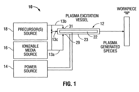
[00441 Referring initially to Fig. 1, a plasma system 10 is disclosed. The
system 10
includes a plasma device 12 that is coupled to a power source 14, an ionizable
media source
16 and a precursor source 18. Power source 14 includes any suitable components
for
delivering power or matching impedance to plasma device 12. More particularly,
the power
source 14 may be any radio frequency generator or other suitable power source
capable of
producing power to ignite the ionizable media to generate plasma. The plasma
device 12
may be utilized as an electrosurgical pencil for application of plasma to
tissue and the power
9
CA 02763868 2011-11-29
WO 2010/138103 PCT/US2009/005389
source 14 may be an electrosurgical generator that is adapted to supply the
device 12 with
electrical power at a frequency from about 0.1 MHz to about 2,450 MHz and in
another
embodiment from about 1 MHz to about 13.56 MHz. The plasma may also be ignited
by
using continuous or pulsed direct current (DC) electrical energy.
[0045] The precursor source 18 may be a bubbler or a nebulizer configured to
aerosolize precursor feedstocks prior to introduction thereof into the device
12. The precursor
source 18 may also be a micro droplet or injector system capable of generating
predetermined
refined droplet volume of the precursor feedstock from about 1 femtoliter to
about 1 nanoliter
in volume. The precursor source 18 may also include a microfluidic device, a
piezoelectric
pump, or an ultrasonic vaporizer.
[0046] The system 10 provides a flow of plasma through the device 12 to a
workpiece
"W" (e.g., tissue). Plasma feedstocks, which include ionizable media and
precursor
feedstocks, are supplied by the ionizable media source 16 and the precursor
source 18,
respectively, to the plasma device 12. During operation, the precursor
feedstock and the
ionizable media are provided to the plasma device 12 where the plasma
feedstocks are ignited
to form plasma effluent containing ions, radicals, photons from the specific
excited species
and metastables that carry internal energy to drive desired chemical reactions
in the
workpiece "W" or at the surface thereof. The feedstocks may be mixed upstream
from the
ignition point or midstream thereof (e.g., at the ignition point) of the
plasma effluent, as
shown in Fig. I and described in more detail below.
[0047] The ionizable media source 16 provides ionizable feedstock to the
plasma
device 12. The ionizable media source 16 is coupled to the plasma device 12
and may
include a storage tank and a pump (not explicitly shown). The ionizable media
may be a
liquid or a gas such as argon, helium, neon, krypton, xenon, radon, carbon
dioxide, nitrogen,
CA 02763868 2011-11-29
WO 2010/138103 PCT/US2009/005389
hydrogen, oxygen, etc. and their mixtures, and the like, or a liquid. These
and other gases
may be initially in a liquid form that is gasified during application.
[00481 The precursor source 18 provides precursor feedstock to the plasma
device 12.
The precursor feedstock may be either in solid, gaseous or liquid form and may
be mixed
with the ionizable media in any state, such as solid, liquid (e.g.,
particulates or droplets), gas,
and the combination thereof. The precursor source 18 may include a heater,
such that if the
precursor feedstock is liquid, it may be heated into gaseous state prior to
mixing with the
ionizable media.
In one embodiment, the precursors may be any chemical species capable of
forming reactive
species such as ions, electrons, excited-state (e.g., metastable) species,
molecular fragments
(e.g., radicals) and the like, when ignited by electrical energy from the
power source 14 or
when undergoing collisions with particles (electrons, photons, or other energy-
bearing
species of limited and selective chemical reactivity) formed from ionizable
media 16. More
specifically, the precursors may include various reactive functional groups,
such as acyl
halide, alcohol, aldehyde, alkane, alkene, amide, amine, butyl, carboxlic,
cyanate, isocyanate,
ester, ether, ethyl, halide, haloalkane, hydroxyl, ketone, methyl, nitrate,
nitro, nitrile, nitrite,
nitroso, peroxide, hydroperoxide, oxygen, hydrogen, nitrogen, and combination
thereof. In
embodiments, the chemical precursors may be water, halogenoalkanes, such as
dichloromethane, tricholoromethane, carbon tetrachloride, difluoromethane,
trifluoromethane, carbon tetrafluoride, and the like; peroxides, such as
hydrogen peroxide,
acetone peroxide, benzoyl peroxide, and the like; alcohols, such as methanol,
ethanol,
isopropanol, ethylene glycol, propylene glycol, alkalines such as NaOH, KOH,
amines,
alkyls, alkenes, and the like. Such chemical precursors may be applied in
substantially pure,
mixed, or soluble form.
11
CA 02763868 2011-11-29
WO 2010/138103 PCT/US2009/005389
[0049] The precursors and their functional groups may be delivered to a
surface to
react with the surface species (e.g., molecules) of the workpiece "W." In
other words, the
functional groups may be used to modify or replace existing surface
terminations of the
workpiece "W." The functional groups react readily with the surface species
due to their
high reactivity and the reactivity imparted thereto by the plasma. In
addition, the functional
groups are also reacted within the plasma volume prior to delivering the
plasma volume to
the workpiece.
[0050] Some functional groups generated in the plasma can be reacted in situ
to
synthesize materials that subsequently form a deposition upon the surface.
This deposition
may be used for stimulating healing, killing bacteria, and increasing
hydrophilic or
hydroscopic properties. In addition, deposition of certain function groups may
also allow for
encapsulation of the surface to achieve predetermined gas/liquid diffusion,
e.g., allowing gas
permeation but preventing liquid exchange, to bond or stimulate bonding of
surfaces, or as a
physically protective layer.
[0051] The precursor source 18 and the ionizable media source 16 may be
coupled to
the plasma device 12 via tubing 13a and 13b, respectively. The tubing 13a and
13b may be
combined into tubing 13c to deliver a mixture of the ionizable media and the
precursor
feedstock to the device 12 at a proximal end thereof. This allows for the
plasma feedstocks,
e.g., the precursor feedstock and the ionizable gas, to be delivered to the
plasma device 12
simultaneously prior to ignition of the mixture therein.
[0052] In another embodiment, the ionizable media source 16 and the precursors
source 18 may be coupled to the plasma device 12 via the tubing 13a and 13b at
separate
connections, e.g., the first connection 31 and a second connection 29,
respectively, such that
the mixing of the feedstocks occurs within the plasma device 12 upstream from
the ignition
point. In other words, the plasma feedstocks are mixed proximally of the
ignition point,
12
CA 02763868 2011-11-29
WO 2010/138103 PCT/US2009/005389
which may be any point between the respective sources 16 and 18 and the plasma
device 12,
prior to ignition of the plasma feedstocks to create the desired mix of the
plasma effluent
species for each specific surface treatment on the workpiece "W."
[0053] In a further embodiment, the plasma feedstocks may be mixed midstream,
e.g.,
at the ignition point or downstream of the plasma effluent, directly into the
plasma. More
specifically, the first and second connections 31, 29 may be coupled to the
device 12 at the
ignition point, such that the precursor feedstocks and the ionizable media are
ignited
concurrently as they are mixed (Fig. 1). It is also envisioned that the
ionizable media may be
supplied to the device 12 proximally of the ignition point, while the
precursor feedstocks are
mixed therewith at the ignition point.
[0054] In a further illustrative embodiment, the ionizable media may be
ignited in an
unmixed state and the precursors may be mixed directly into the ignited
plasma. Prior to
mixing, the plasma feedstocks may be ignited individually. The plasma
feedstock is supplied
at a predetermined pressure to create a flow of the medium through the device
12, which aids
in the reaction of the plasma feedstocks and produces a plasma effluent. The
plasma
according to the present disclosure is generated at or near atmospheric
pressure under normal
atmospheric conditions.
[0055] With reference to Figs. 1-3, the device 12 includes an inner electrode
22
disposed coaxially within an outer electrode 23. As shown in Fig. 2A, the
outer electrode 23
has a substantially cylindrical tubular -shape having an opening 25 (Fig. 3)
defined therein.
The inner electrode 22 has a substantially cylindrical shape (e.g., rod-
shaped). The electrodes
22 and 23 may be formed from a conductive material suitable for ignition of
plasma such as
metals and metal-ceramic composites. In one embodiment, the electrodes 22 and
23 may be
formed from a conductive metal including a native oxide or nitride compound
disposed
thereon.
13
CA 02763868 2011-11-29
WO 2010/138103 PCT/US2009/005389
[00561 The device 12 also includes an electrode spacer 27 disposed between the
inner
and outer electrodes 22 and 23. The electrode spacer 27 may be disposed at any
point
between the inner and outer electrodes 22 and 23 to provide for a coaxial
configuration
between the inner and outer electrodes 22 and 23. The electrode spacer 27
includes a central
opening 40 adapted for insertion of the inner electrode 22 therethrough and
one or more flow
openings 42 disposed radially around the central opening 40 to allow for the
flow of ionizable
media and precursors through the device 12. The electrode spacer 27 may be
frictionally
fitted to the electrodes 22 and 23 to secure the inner electrode 22 within the
outer electrode
23. In another embodiment, the electrode spacer 27 is slidably disposed over
the inner
electrode 22. In one illustrative embodiment, the electrode spacer 27 may be
formed from a
dielectric material, such as ceramic, to provide capacitive coupling between
the inner and
outer electrodes 22 and 23.
[00571 As shown in Fig. 2B, distal end of the inner electrode 22 may extend
past the
distal end of the outer electrode 23. In another embodiment, as shown in Figs.
2C and 2D,
the inner electrode 22 may be fully enclosed by the outer electrode 23. In
particular, the
distal end the inner electrode 22 may be flush with the distal end of the
outer electrode 23
(Fig. 2C). In a further embodiment, the inner electrode 22 may be recessed
within the outer
electrode 23 (e.g., distal end of the inner electrode 22 is within the opening
25 as shown in
Fig. 2D).
100581 The extended distance of the inner electrode 22 relative to the outer
electrode
23 may be adjusted to achieve a desired spatial relationship between the
electrodes 22 and 23.
In one embodiment, the electrode spacer 27 is secured to the outer electrode
23 but is slidably
disposed over the inner electrode 22. In other words, the inner electrode 22
may move
through the opening 40. This allows for the outer electrode 23 and the
electrode spacer 27 to
be longitudinally movable along the inner electrode 22 thereby controlling the
exposure of
14
CA 02763868 2011-11-29
WO 2010/138103 PCT/US2009/005389
the distal end of the inner electrode 22. In another embodiment, the inner and
outer
electrodes 22 and 23 may be fixated in a coaxial configuration using other
fixation
mechanisms (e.g., clamps) that allow for adjustment of the exposure distance
of the inner
electrode 22.
[0059] One of the electrodes 22 and 23 may be an active electrode and the
other may
be a neutral or return electrode to facilitate in RF energy coupling. Each of
the electrodes 22
and 23 are coupled to the power source 14 that drives plasma generation and
electron sheath
formation close to the inner electrode 22, such that the energy from the power
source 14 may
be used to ignite the plasma feedstocks flowing through the device 12. More
specifically, the
ionizable media and the precursors flow through the device 12 through the
opening 25 (e.g.,
through the electrode spacer 27 and between the inner and outer electrodes 22
and 23). The
inner electrode 22 may also include one or more openings (not explicitly
shown)
therethrough to facilitate the flow of ionizable media and the precursors.
When the
electrodes 22 and 23 are energized, the plasma feedstocks are ignited and form
a plasma
effluent which is emitted from the distal end of the device 12 onto the
workpiece "W."
[0060] As shown in Fig. 3, the inner electrode 22 includes a coating 24 that
covers at
least a portion of the inner electrode 22 leaving an exposed (e.g.,
uninsulated or uncoated)
distal portion 27 of the inner electrode 22 uninsulated. In another
embodiment, the coating
24 may be disposed on the outer electrode 23 as discussed in more detail below
with respect
to Figs. 4-7 and 16.
[0061] The coating 24 may be formed from an insulative or semiconductive
material
deposited as a film unto the inner conductor (e.g., atomic layer deposition)
or as a dielectric
sleeve or layer. In one illustrative embodiment, the insulative cover 24 may
be a native metal
oxide. The coating 24 limits the plasma action to the distal portion 27 and
provides for the
creation of a plasma effluent 31 having an energetic electron sheath layer 33.
The sheath
CA 02763868 2011-11-29
WO 2010/138103 PCT/US2009/005389
layer 33 has a reaching distance "d" from about 1 to about 10 mm, suitable for
contacting the
sheath layer 33 to the workpiece "W" to promote volatilization and/or
modification of
chemical bonds at the surface thereof as discussed in more detail below with
respect to Figs.
16-24.
[0062] In addition, the coating 24 provides for capacitive coupling between
the inner
and outer electrodes 22 and 23. The resulting capacitive circuit element
structure provides
for a net negative bias potential at the surface of the inner electrode 22,
which attracts the
ions and other species from the plasma effluent. These species then bombard
the coating 24
and release the electrons generating the sheath layer 33.
[0063] The sheath layer 33 is generated in part by the materials of the
electrodes 22
and 23 and in particular by the coating 24. Materials having high secondary
electron
emission property, y, in response to ion and/or photon bombardment are
suitable for this task.
Such materials include insulators and/or semiconductors. These materials have
a relatively
high y, where y represents the number of electrons emitted per incident
bombardment
particle. Thus, metals generally have a low y (e.g., less than 0.1) while
insulative and
semiconductor materials, such as metallic oxides have a high y, from about I
to about 10 with
some insulators exceeding a value of 20. Thus, the coating 24 acts as a source
of secondary
emitted electrons, in addition to limiting the plasma to the distal end of the
inner electrode 22.
[0064] Secondary electron emission, y, may be described by the formula (1):
(1) rsecondary/ l' ion
[0065] In formula (1) y is the secondary electron emission yield or
coefficient,
Fsecondary is the electron flux, and Fion is the ion flux. Secondary emission
occurs due to the
impacts of plasma species (ions) onto the coating 24.when the ion impact
collisions have
16
CA 02763868 2011-11-29
WO 2010/138103 PCT/US2009/005389
sufficient energy to induce secondary electron emission, thus generating y-
mode discharges.
Generally discharges are said to be in y-mode when electron generation occurs
preferentially
at electrode surfaces (i.e., y > 1) instead of in the gas (an a-mode
discharge). In other words,
per each ion colliding with the coating 24, a predetermined number of
secondary electrons
are emitted. Thus, y may also be thought of as a ratio of the rseconda ,
(e.g., the electron flux)
and F;oõ (e.g., the ion flux).
[0066] These ion collisions with the surface of the coating 24, in turn,
provide
sufficient energy for secondary electron emission to generate y discharges.
The ability of
coating materials such as coating 24 to generate y discharges varies with
several parameters,
with the most influence due to the choice of materials having a high y as
discussed above.
This property allows coatings 24 to act as a source of secondary emitted
electrons or as a
catalytic material to enhance selected chemical reaction paths.
[0067] Over time the coating 24 may thin or be removed during the plasma
operation.
In order to maintain the coating 24 to continually provide a source of
secondary emitted
electrons, the coating 24 may be continually replenished during the plasma
operation. This
may be accomplished by adding species that reformulate the native coating 24
on the inner
and outer electrodes 22 and 23. In one embodiment, the precursor source 18 may
provide
either oxygen or nitrogen gas to the device 12 to replenish to oxide or
nitride coating.
[0068] Generation of the sheath layer 33 is also controlled by the supply of
the
ionizable media and the precursors. Ionizable media and the precursors are
selected that are
relatively transparent to the energetic electrons released during secondary
emission from the
surface of the inner electrode 22. As stated above, the plasma is generated at
atmospheric
pressure. Due to the increased entropy at such pressure, the generated
electrons undergo a
multitude of collisions in a relatively short period of time and space forming
the sheath layer
33.
17
CA 02763868 2011-11-29
WO 2010/138103 PCT/US2009/005389
[0069] The thickness of the sheath layer 33 is defined by a formula (2):
(2) Thickness = 1/Na
[0070] In formula (2), N is the number of scattering centers, which may be the
molecules of the ionizable media, the precursors and the atmospheric gases.
Thus, N defines
the media density. The variable, a, is the average particle cross-section of
the scattering
centers. The thickness of the sheath layer 33 is inversely proportional to the
product of N and
a. Thus, decreasing N and a allows for achieving a thicker sheath layer 33. A
lower a may
be provided by using specific ionizable media compounds with molecules having
a low
cross-section, such as hydrogen and helium. The variable N may be lowered by
heating the
ionizable media to reduce the gas density and limiting the amount of media
provided to the
lowest amount needed to sustain the plasma reaction.
[0071] The present disclosure also relates to systems and methods for
generating
plasma effluents having the energetic electron sheath layer having a reaching
distance "d."
The sheath layer 33 is produced by the combination of disclosed electrode
structures, specific
gas species, electrode materials, proper excitation conditions, and other
media parameters.
The propagation of energetic electron for mm-sized distances provides for
practical
applications on a variety of surfaces, such as modification of chemical bonds
on the surface
and volatilization of surface compounds.
[0072] In another embodiment as shown in Figs. 4-6, the coating 24 is disposed
on
the outer surface of the inner electrode 22 and on the inner surface of the
outer electrode 23.
In other words, the surfaces of the inner and outer electrodes 22 and 23
facing the opening 25
include the coating 24. In one embodiment, the coating 24 may cover the entire
surface of the
inner and outer electrodes 22 and 23 (e.g., outer and inner surface thereof,
respectively). In
18
CA 02763868 2011-11-29
WO 2010/138103 PCT/US2009/005389
another embodiment, the coating 24 may cover only a portion of the electrodes
22 and 23,
such as a distal, proximal (e.g., Fig. 3 illustrates an uncoated distal
portion 27) or middle
portions thereof.
[0073] The coating 24 may be a native oxide, or a native nitride of the metal
from
which the inner and outer electrodes are formed, or may be a deposited layer
or a layer
formed by ion implantation. In one illustrative embodiment, the inner and
outer electrodes 22
and 23 are formed from an aluminum alloy and the coating 24 is aluminum oxide
(A1203) or
aluminum nitride (A1N). In another illustrative embodiment, the inner and
outer electrodes 22
and 23 are formed from a titanium alloy and the coating 24 is titanium oxide
(Ti02) or
titanium nitride (TiN).
[0074] The inner and outer electrodes 22 and 23 and the coating 24 may also be
configured as a heterogeneous system. The inner and outer electrodes 22 and 23
may be
formed from any suitable electrode substrate material (e.g., conductive metal
or a semi-
conductor) and the coating 24 may be disposed thereon by various coating
processes. The
coating 24 may be formed on the inner and outer electrodes 22 and 23 by
exposure to an
oxidizing environment, anodization, electrochemical processing, ion
implantation, or
deposition (e.g., sputtering, chemical vapor deposition, atomic layer
deposition, etc.).
[0075] In another embodiment the coating 24 on electrodes 22 and 23 may be
different on each electrode and may serve separate purposes. One coating 24
(e.g., on the
electrode 22) can be selected to promote increased secondary electron emission
while coating
24 on the other electrode (e.g., electrode 23) can be selected to promote
specific chemical
reactions (e.g., act as a catalyst).
[0076] As shown in Figs. 5 and 6, the coating 24 may also include a plurality
of
nanostructure pores 60, which may be arranged in a predetermined (e.g.,
unidirectional) form
(Fig. 5) or in a random configuration (Fig. 6): Pores 60 may be formed during
the coating
19
CA 02763868 2011-11-29
WO 2010/138103 PCT/US2009/005389
processes discussed above. In one illustrative embodiment, the pores 60 may be
treated to
include one or more types of precursor feedstock 62 disposed therein. This
allows for
feeding of the precursor feedstock 62 directly into the plasma effluent either
as a substitute
for the precursor source 18 or in conjunction therewith. The precursor
feedstock 62 may be
the precursors discussed above with respect to the precursor source 18. In one
embodiment,
the precursor feedstock 62 may be a catalyst suitable for initiation of the
chemical reactions
between the precursor feedstock supplied from the precursor source 18 and the
plasma.
[00771 Fig. 7 shows a side cross-sectional view of a plasma device 41 having
an inner
electrode 42 disposed coaxially within an outer electrode 43. The outer
electrode 43 has a
substantially cylindrical tubular shape having an opening 45 defined therein.
The inner
electrode 42 has a substantially cylindrical shape and may be fully enclosed
by the outer
electrode 43 or extend past the distal end of the outer electrode 43.
[00781 The device 41 also includes an electrode spacer (not explicitly shown)
disposed between the inner and outer electrodes 42 and 43, similar to the
electrode spacer 27.
The electrode spacer may be disposed at any point between the inner and outer
electrodes 42
and 43 to provide for a coaxial configuration between the inner and outer
electrodes 42 and
43. The electrode spacer may be frictionally fitted to the electrodes 42 and
43 to secure the
inner electrode 42 within the outer electrode 43. In one illustrative
embodiment, the
electrode spacer may be formed from a dielectric material, such as ceramic, to
provide for
capacitive coupling between the inner and outer electrodes 42 and 43.
[00791 Each of the inner and outer electrodes 42 and 43 may include a
plurality of
geometrical arrangements. In one embodiment, as shown in Fig. 7, the inner and
outer
electrodes 42 and 43 include a plurality of grooves 55 disposed on the surface
thereof. The
grooves 55 enhance the local electrical fields along the inner and outer
electrodes 42 and 43.
The grooves 55 may also be covered by a groove coating 50, which is
substantially similar to
CA 02763868 2011-11-29
WO 2010/138103 PCT/US2009/005389
the coating 24 for similar functional purposes. The grooves 55 are disposed on
the outer
surface of the inner electrode 42 and on the inner surface of the outer
electrode 43. The inner
and outer electrodes 42 and 43 and the coating 50 may be formed from the
materials
discussed above with respect to the inner and outer electrodes 22 and 23. In
one
embodiment, the groove coating 50 may be formed from substantially similar
materials as the
coating 24, namely, a combination of aluminum, magnesium, or titanium metals,
and oxides
or nitrides thereof.
[0080] The grooves 55 may be arranged in parallel with a longitudinal axis
defined by
the inner and outer electrodes 42 and 43. In another embodiment, the grooves
45 may be
arranged in a spiral configuration (e.g., rifled) on the inner and outer
electrodes 42 and 43.
The inner electrode 43 may also include one or more side vents 49 to allow for
additional gas
flow into the opening 45.
[0081] The present disclosure provides for a variety of plasma device
embodiments
and configurations suitable for wide area plasma treatment of tissue. Common
to the
disclosed embodiments is the uniform dispersion of plasma feedstocks in the
vicinity of both
active and return electrodes employed. In one embodiment, the plasma
conditions provide
for a plasma media that flows in a laminar form within plasma device 12.
[0082] Fig. 8 shows a plasma device 112 includes an inner electrode 122 having
a
substantially cylindrical tubular shape having an opening 125 defined
therethrough. The
inner electrode 122 has a distal end 126 and proximal end 124 that is coupled
to the ionizable
media source 16 and the precursor source 18 (Fig. 1). The inner electrode 122
is also coupled
to a porous member 128 at the distal end 126. The porous member 128 disperses
the plasma
passing through the inner electrode 122 to generate a wide-area plasma
effluent 129. The
inner electrode 122 may have an inner diameter a of 10 cm or less. The porous
member 128
may be formed from sintered or metal glass, ceramic mesh, and other porous
materials
21
CA 02763868 2011-11-29
WO 2010/138103 PCT/US2009/005389
suitable for dispersion of gas. The porous member 128 may have a thickness b
from about
0.1 to about 1.0 cm.
[0083] The plasma device 112 also includes an outer electrode 123 that also
has a
substantially cylindrical tubular or annular shape having a larger diameter
than the diameter
of the inner electrode 122. The inner and outer electrodes 122 and 123 are
concentrically
disposed about a longitudinal axis A-A. The outer electrode 123 has a shorter
length than the
inner electrode 122 and is disposed coaxially about the inner electrode 122.
In particular, the
outer electrode 123 encloses a distal portion 130 of the inner electrode 122
and the porous
member 128.
[0084] The electrodes 122 and 123 may be formed from an electrically
conductive or
semi-conducting material suitable for ignition of plasma such as metals and
metal-ceramic
composites. In one embodiment, the electrodes 122 and 123 may be formed from a
conductive metal including a native oxide or nitride compound disposed
thereon.
[0085] The plasma device 112 also includes a dielectric spacer 132 having puck-
like
or toroidal shape. The dielectric spacer 132 includes an opening 134 through
the center
thereof that is adapted for insertion of the inner electrode 122 therethrough.
The dielectric
spacer 132 is disposed between the inner and outer electrodes 122 and 123. In
one
embodiment, the dielectric spacer 132 may be frictionally fitted to the
electrodes 122 and 123
to secure the inner electrode 122 within the outer electrode 123. The
dielectric spacer may
have a thickness c from about 0.1 to about 1.0 cm (e.g., gauge). In one
illustrative
embodiment, the electrode spacer 132 may be formed from a dielectric material,
such as a
thin ceramic, to provide capacitive coupling between the inner and outer
electrodes 122 and
123.
[0086] One of the electrodes 122 and 123 may be an active electrode and the
other
may be a neutral or return electrode to facilitate in RF energy coupling. Each
of the
22
CA 02763868 2011-11-29
WO 2010/138103 PCT/US2009/005389
electrodes 122 and 123 are coupled to the power source 14 that drives plasma
generation,
such that the energy from the power source 14 may be used to ignite and
sustain the plasma
in feedstocks 127 flowing through the device 112 (e.g., through the opening
125).
[0087] Fig. 9 shows another illustrative embodiment of a plasma device 212
which
includes a housing 211 enclosing a first electrode 222 and a second electrode
223 separated
by a predetermined distance d, which may be from about 0.1 cm to about 1 cm.
The first
electrode 222 is proximal of the second electrode 223 with respect to the
supplied plasma
feedstocks. The housing 211 has a substantially cylindrical tubular shape
having an opening
225 defined therethrough. The housing 211 is formed from a dielectric material
that insulates
the first and second electrodes 222 and 223. The housing 211 may have an inner
diameter e
of 10 cm or less.
[0088] The plasma device 212 includes a distal end 226 and proximal end 224
that is
coupled to the ionizable media source 16 and the precursor source 18. The
first and second
electrodes 222 and 223 are formed from conductive porous material, such as
metal, metal-
ceramic and semi-conducting composite meshes, porous sintered solids, and the
like to permit
the flow of plasma feedstocks 228 therethrough. The first and second
electrodes 222 and 223
disperse the plasma passing through the housing 211 to generate a dispersed
wide-area
plasma effluent 229.
[0089] One of the electrodes 222 and 223 may be an active electrode and the
other
may be a neutral or return electrode to facilitate in RF energy coupling. Each
of the
electrodes 222 and 223 are coupled to- the power source 14 that drives plasma
generation,
such that the energy from the power source 14 may be used to ignite the plasma
feedstocks
flowing through the device 212. The electrodes 222 and 223 are separated by a
predetermined distance and are capacitively or inductively coupled through the
plasma
effluent 229 and the housing 211. More specifically, the ionizable media and
the precursors
23
CA 02763868 2011-11-29
WO 2010/138103 PCT/US2009/005389
flow through the device 212 through the chambered opening 225. As energy is
applied to the
electrodes 222 and 223, the plasma feedstocks are ignited to form the plasma
effluent 229.
[00901 Fig. 10 shows another illustrative embodiment of a plasma device 312
which
includes a housing 311 enclosing a first electrode 322 and a second electrode
323. The
housing 311 has a substantially cylindrical tubular shape having a chambered
opening 325
defined therethrough. The housing 311 is formed from a dielectric material
that insulates the
first and second electrodes 322 and 323. The housing 311 may have an inner
diameter f of 10
cm or less.
100911 The plasma device 312 includes a distal end 326 and proximal end 324
that is
coupled to the ionizable media source 16 and the precursor source 18. The
first electrode 322
may be a cylindrical rod formed from a conductive metal (e.g., aluminum alloy)
or
semiconductive material, disposed coaxially within the housing 311.
[00921 The plasma device 312 also includes an electrode spacer 327 disposed
between first electrode 322 and the housing 311. The electrode spacer 327 is
substantially
similar to the electrode spacer 27 and may include a central opening 340
adapted for insertion
of the inner electrode 322 therethrough and one or more flow openings 342
disposed radially
around the central opening to allow for the flow of plasma feedstocks 328
(e.g., ionizable
media and precursors) through the device 312. The electrode spacer 327 may be
frictionally
fitted to the housing 311 and the first electrode 322 to secure the first
electrode 22 within the
housing 311. In one illustrative embodiment, the electrode spacer 327 may be
formed from a
dielectric material, such as ceramic. In another embodiment, the electrode
spacer 327 may be
formed integrally with the housing 311.
[00931 The first electrode 322 also includes an insulative layer 343, which
may be
formed integrally with the housing 311 and the electrode spacer 327. In
another illustrative
embodiment, the layer 343 may be formed from a dielectric material deposited
as a film unto
24
CA 02763868 2011-11-29
WO 2010/138103 PCT/US2009/005389
or grown on the inner conductor via processes including, but not limited to,
sputtering,
chemical vapor (e.g., atomic layer deposition, evaporation, electrochemical
methods, or ion
implantation.). The insulative layer 343 may also be a native metal oxide or
nitride if the first
electrode 332 is formed from a suitable alloy, such as aluminum and titanium.
In particular,
the first electrode 322 may be formed from an aluminum alloy and the layer 342
may be
aluminum oxide (A1203) or aluminum nitride (A1N). In another illustrative
embodiment, the
first electrode 322 may be formed from a titanium alloy and the layer 342 may
be titanium
oxide (Ti02) or titanium nitride (TiN).
[0094] The second electrode 323 is formed from a conductive or semiconductive
porous material, such as metal and metal-ceramic composite meshes, porous
sintered solids
and the like to permit the flow of plasma feedstocks 328 therethrough. The
second electrode
323 also disperses the plasma passing through the housing 311 to generate a
wide-area
plasma effluent 329.
[0095] One of the electrodes 322 and 323 may be an active electrode and the
other
may be a neutral or return electrode to facilitate in RF energy coupling. Each
of the
electrodes 322 and 323 are coupled to the power source 14 that drives plasma
generation,
such that the energy from the power source 14 may be used to ignite the plasma
feedstocks
flowing through the device 312. The electrodes 322 and 323 are capacitively or
inductively
coupled through the plasma effluent 329 and the housing 311. More
specifically, the
ionizable media and the precursors flow through the device 312 through the
chambered
opening 325. As energy is applied to the electrodes 322 and 323, the plasma
feedstocks are
ignited to form the plasma effluent 329.
[0096] Figs. 11 A - C show another illustrative embodiment of a plasma device
412
which includes a housing 411 and a dielectric spacer 432 having disk-like or
toroidal shape
disposed within the housing 411. The dielectric spacer 432 may be frictionally
fitted to the
CA 02763868 2011-11-29
WO 2010/138103 PCT/US2009/005389
housing 411. In one illustrative embodiment, the dielectric spacer 432 may be
formed
integrally with the housing 411.
[0097] The dielectric spacer 432 includes a bottom surface 426 and a top
surface 424
that is coupled to the ionizable media source 16 and the precursor source 18
(Fig. 1). The
electrode spacer 432 may be formed from a dielectric material, such as
ceramic, plastic, and
the like. The dielectric spacer 432 includes one or more openings 434 through
the center
thereof to allow for the flow of plasma feedstocks 428 therethrough. In one
illustrative
embodiment, the dielectric spacer 432 may be formed from a porous dielectric
media suitable
for allowing gases to flow therethrough thereby obviating the need for
openings 434. The
multiple openings 434 and/or porous nature of the dielectric spacer 432
provide for
dispersion of the plasma passing therethrough to generate a wide-area plasma
effluent 429.
The openings 434 may be of various shapes and sizes. Fig. 11 B shows the
openings 434 as
slits formed in the dielectric spacer 432. Fig. 11 C shows the openings 434 as
substantially
cylindrical lumens. At its widest thickness g, the openings 434 may be from
about 0.1 cm to
about 1.0 cm.
[0098] The plasma device 412 also includes first and.second electrodes 422 and
423
disposed within the dielectric spacer 432. The first and second electrodes 422
and 423 may
be cylindrical rods, formed from a conductive metal (e.g., aluminum alloy) and
may be
inserted into the dielectric spacer 432 in parallel configuration and
equidistant from the center
of the dielectric spacer 432. The dielectric spacer 432 provides capacitive
coupling between
the inner and outer electrodes 422 and 423. In one embodiment electrodes 422
and 423 may
have one or more regions that form and present sharpened protuberances toward
openings
434 to increase the local electric fields.
[0099] One of the electrodes 422 and 423 may be an active electrode and the
other
may be a neutral or return electrode to facilitate in RF energy coupling. Each
of the
26
CA 02763868 2011-11-29
WO 2010/138103 PCT/US2009/005389
electrodes 422 and 423 are coupled to the power source 14 that drives plasma
generation,
such that the energy from the power source 14 may be used to ignite the plasma
feedstocks
flowing through the device 412. The electrodes 422 and 423 are capacitively
coupled
through the plasma effluent 429 and the dielectric spacer 432. More
specifically, the
ionizable media and the precursors flow through the device 412 through the
openings 434.
As energy is applied to the electrodes 422 and 423, the plasma feedstocks are
ignited to form
the plasma effluent 429.
[001001 Figs. 12A - B show another illustrative embodiment of a plasma device
512
which includes a dielectric spacer 532 having a substantially disk shape. The
plasma device
512 includes a bottom surface 526 and a top surface 524 that is coupled to the
ionizable
media source and the precursor source 18 (Fig. 1). The electrode spacer 532
may be formed
from a dielectric material, such as ceramic, plastic, and the like. In one
illustrative
embodiment, the dielectric spacer 532 may be formed from a porous dielectric
media suitable
for allowing gases to flow therethrough, or otherwise have open ports to allow
flow of plasma
feedstocks 528 through the plasma device 512. The electrode spacer 532 may
have a
thickness h from about 0.1 cm to about 1.0 cm.
[001011 The plasma device 512 also includes first and second electrodes 522
and 523.
The first and second electrodes 522 and 523 may also have a disk or plate
shape and are
disposed on the top and bottom surfaces 524 and 526, respectively. The first
and second
electrodes 522 and 523 are formed from a conductive or semiconductive porous
material,
such as metal and metal-ceramic composite meshes, porous sintered solids, and
the like to
permit the flow of plasma feedstocks 528 therethrough, or otherwise have open
ports to allow
flow of plasma feedstocks 528 through the plasma device 512. The first and
second
electrodes 522 and 523 may have a diameter i from about 0.1 cm to about 1.0 cm
and a
thickness j from about 0.1 cm to about 1.0 cm.
27
CA 02763868 2011-11-29
WO 2010/138103 PCT/US2009/005389
[001021 The dielectric spacer 532 may have a larger diameter extending outside
the
periphery of the first and second electrodes 522 and 523, such that a border k
is formed,
which may be from about 0.1 cm to about 1.0 cm. This configuration enhances
capacitive
coupling between the inner and outer electrodes 522 and 523. One or both of
electrodes 522
and 523 may also be formed into predetermined surface shapes and features to
induce effects
such as inductive coupling. The porous nature of the dielectric spacer 532 in
conjunction
with the first and second electrodes 522 and 523 provides for dispersion of
the plasma
passing therethrough to generate a wide-area plasma effluent 529.
[001031 One of the electrodes 522 and 523 may be an active electrode and the
other
may be a neutral or return electrode to facilitate in RF energy coupling. Each
of the
electrodes 522 and 523 are coupled to the power source 14 that drives plasma
generation,
such that the energy from the power source 14 may be used to ignite the plasma
feedstocks
528 flowing through the device 512. The ionizable media and the precursors
flow through
the device 512 and as energy is applied to the electrodes 522 and 523, the
plasma feedstocks
are ignited to form the plasma effluent 529.
[001041 Fig. 13 shows another illustrative embodiment of a plasma device 612,
which
is a combination of the plasma device 212 of Fig. 9 and plasma device 512 of
Fig. 12. The
plasma device 612 includes a housing 611 enclosing a dielectric spacer 632
having disk
shape, a first electrode 622 and a second electrode 623. The housing 611 may
have an inner
diameter 1 of 10 cm or less. The plasma device 612 includes a bottom surface
626 and a top
surface 624 that is coupled to the ionizable media source 16 and the precursor
source 18 (Fig.
1). The dielectric spacer 632 may be formed from a dielectric material, such
as ceramic,
plastic, and the like. In one illustrative embodiment, the dielectric spacer
632 may be formed
from a porous dielectric media suitable for allowing gases to flow
therethrough. The
dielectric spacer 632 has a thickness m from about 0.1 cm to about 1.0 cm.
28
CA 02763868 2011-11-29
WO 2010/138103 PCT/US2009/005389
[001051 The first and second electrodes 622 and 623 may also have a disk or
plate
shape and are disposed on the top and bottom surfaces 627 and 629,
respectively. The first
and second electrodes 622 and 623 have a thickness n from about 0.1 cm to
about 1.0 cm and
are formed from a conductive porous material, such as metal and metal-ceramic
composite
meshes, porous sintered solids, and the like to permit the flow of plasma
feedstocks 628
therethrough. The porous nature of the dielectric spacer 632 in conjunction
with the first and
second electrodes 622 and 623 provides for dispersion of the plasma passing
therethrough to
generate a wide-area plasma effluent 629. The dielectric spacer 632 also
provides for
capacitive coupling between the inner and outer electrodes 622 and 623.
[001061 One of the electrodes 622 and 623 may be an active electrode and the
other
may be a neutral or return electrode to facilitate in RF energy coupling. Each
of the
electrodes 622 and 623 are coupled to the power source 14 that drives plasma
generation,
such that the energy from the power source 14 may be used to ignite and
sustain the plasma
feedstocks 628 flowing through the device 612. In one embodiment one electrode
may be a
solid and the second electrode formed into a spiral or other highly inductive
form to achieve
inductive coupling. The ionizable media and the precursors 628 flow through
the device 612
and as energy is applied to the electrodes 622 and 623, the plasma feedstocks
are ignited to
form the plasma effluent 629.
[001071 Figs. 14 and 15 show an illustrative embodiment of a plasma system
1100.
The system 1100 includes a plasma device 1112 that is coupled to a power
source 1114, an
ionizable media source 1116 and a precursor source 1118. Power source 1114
includes a
signal generator 1250 coupled to an amplifier 1252. The signal generator 1250
outputs a
plurality of control signals to the amplifier 1252 reflective of the desired
waveform. The
signal generator 1250 allows for control of desired waveform parameters (e.g.,
frequency,
duty cycle, amplitude, pulsing, etc.). In some embodiments, signal generator
1250 may pulse
29
CA 02763868 2011-11-29
WO 2010/138103 PCT/US2009/005389
the waveform, e.g., a continuous-wave waveform signal may be switched on and
off at a duty
cycle (the duty cycle may be fixed or variable) and at a different frequency
from the
frequency of the continuous-wave waveform. The amplifier 1252 outputs the
desired
waveform at a frequency from about 0.1 MHz to about 2,450 MHz and in another
embodiment from about 1 MHz to about 13.56 MHz. The power source 1114 also
includes a
matching network 1254 coupled to the amplifier 1252. The matching network 1254
may
include one or more reactive and/or capacitive components that are configured
to match the
impedance of the load (e.g., plasma effluent) to the power source 1114 by
switching the
components or by frequency tuning.
[001081 The power source 1114 is coupled to a plasma device 1112. As shown in
Fig.
15, the plasma device 1112 may be utilized for application of plasma to
tissue. The device
1112 includes an inner electrode 1122, which may be an aluminum alloy rod,
disposed
coaxially within an outer electrode 1123. The outer electrode 1123 may be an
aluminum
alloy tube having an opening 1125. As shown in Fig. 14, the inner and outer
electrode 1122
and 1123 are coupled to the power source 1114 via connectors 1256 and 1258,
which are
disposed around the inner electrode 1122 and 1123, respectively. The
connectors 1256 and
1258 may be copper connector blocks.
[001091 With reference to Fig. 15, the device 1112 also includes a ceramic
electrode
spacer 1127 disposed between the inner and outer electrodes 1122 and 1123. The
electrode
spacer 1127 may be disposed at any point between the inner and outer
electrodes 1122 and
1123 to provide for a coaxial configuration between the inner and outer
electrodes 1122 and
1123. The electrode spacer 1127 is substantially similar to the electrode
spacer 27 and may
include a central opening (not explicitly shown) adapted for insertion of the
inner electrode
1122 therethrough and one or more flow openings (not explicitly shown)
disposed radially
around the central opening to allow for the flow of plasma feedstocks through
the device
CA 02763868 2011-11-29
WO 2010/138103 PCT/US2009/005389
1112. The electrode spacer 1127 may be frictionally fitted to the electrodes
1122 and 1123 to
secure the inner electrode 1122 within the outer electrode 1123. One of the
electrodes 1122
and 1123 may be an active electrode and the other may be a neutral or return
electrode to
facilitate in RF energy coupling.
[001101 With reference to Fig. 14, the plasma system 1100 also includes an
ionizable
media source 1116 and a precursor source 1118 coupled to the plasma device
1112. The
ionizable media source 1116 provides ionizable feedstock, namely, helium gas,
to the plasma
device 1112. The ionizable media source 1116 includes a storage tank for
storing the helium
gas. The ionizable media source 1116 is coupled to the precursor source 1118
via tubing
1262, which includes tubing 1262a coupled to the ionizable media source 1116.
The tubing
1262a branches into tubing 1262b and 1262c. The tubing 1262c is coupled to the
precursor
source 1118, which may be a bubbler or a nebulizer, for aerosolizing precursor
feedstocks,
namely liquid hydrogen peroxide, prior to introduction thereof into the device
1112. The
feedstocks are mixed upstream of the device 1112 prior to introduction
thereto.
[001111 The tubing 1262b bypasses the tubing 1262c and reconnects at tubing
1262d,
which is coupled to the plasma device 1112 at a coupling 1264. The coupling
1264 may be a
Teflon union tee connected to the outer electrode 1123. The tubing 1262 also
includes valves
1260a, 1260b, 1260c which control the flow of the helium gas and the hydrogen
peroxide
through the tubing 1262a, 1262b, 1262c, respectively. The tubing 1262 further
includes mass
flow controllers 1266b and 1266c adapted to control the flow of plasma
feedstocks through
the tubing 1260b and 1260c, respectively.
[001121 The system 1100 provides a flow of plasma through the device 1112 to
the
tissue. Plasma feedstocks, which include helium gas and hydrogen peroxide, are
supplied by
the ionizable media source 1116 and the precursor source 1118, respectively,
to the plasma
device 1112, which are ignited to form plasma effluent containing ions,
radicals, photons
31
CA 02763868 2011-11-29
WO 2010/138103 PCT/US2009/005389
from the specific excited species and metastables that carry internal energy
to drive desired
chemical reactions with the tissue or at the surface thereof.
[00113] With reference to Fig. 16, a close-up, side view of a plasma device
1112
according to the present disclosure. Plasma device 1112 includes the inner
electrode 1122
and the outer electrode 1123. The plasma device 1112 also includes a coating
1124 disposed
on the outer surface of the inner electrode 1122 and on the inner surface of
the outer electrode
1123. The coating 1124 is substantially similar to the coating 24 that is
discussed above with
respect to Figs. 4-6. In one embodiment, the plasma device 1112 may also
include additional
features discussed above with respect to Figs. 4-6 such as grooves disposed in
a parallel or
spiral configurations, nanostructure pores filled with precursor materials,
and/or vents within
the inner electrode 1122. In another embodiment, the inner electrode 1122 may
be disposed
in a variety of configurations and spatial orientation with respect to the
outer electrode 1123.
In particular, the inner electrode 1122 may be recessed, flush or extended
relative to the outer
electrode 1123 as shown in Figs. 2B - 2D. The extended distance of the inner
electrode 1122
may also be adjustable as discussed above with respect to Figs. 2A - 2D.
[00114] Fig. 16 illustrates working ranges LR,1, LR,2 and LR,3, and a distance
DT. Outer
electrode 1123 includes a working range LR,1 of energetic secondary electron
emissions.
Inner electrode 1122 includes working ranges LR,2, and LR,3 of energetic
secondary electron
emissions having energy E. In other words, the working ranges are
representative of the
thickness of energetic electron sheath layers 1133 and 1134, which are
disposed about the
inner and outer electrodes 1122 and 1123, respectively. A gap distance 0 shows
the zone
where the concentration of energetic secondary electrons is relatively lower.
Coating the
electrodes, as discussed above, reduces gap distance A. In some embodiments,
distance A
may be reduced to zero and/or working ranges LR,I, and LR,2 may overlap
thereby creating an
hollow cathode effect. Inner electrode 1112 includes a tip 1128 having a
distance DT from
32
CA 02763868 2011-11-29
WO 2010/138103 PCT/US2009/005389
tissue "T". Ranges LR,I, LR,2 and LR,3, indicate regions with a greatly
increased concentration
of electrons with relatively high energies that drive reactions in the gas
phase. As discussed
above, the coating 1124 on electrodes 1122 and/or 1123 can increase or enhance
working
ranges LR,1 and LR,2, and/or LR,3 of energetic secondary electrons. Thus,
varying the
thickness of the coating 1124 can be used to adjust the working ranges LR,I
and LR,2, and/or
LR,3. Additionally or alternatively, the distance DT that tip 1128 is disposed
from tissue "T" is
adjustable to achieve a predetermined tissue effect (discussed in more detail
below).
[001151 (3) R(E) =u(E) = ne(E) = v(E).
[001161 Formula (3) relates the reaction rate R that indicates an inelastic
(energy
expending) collision where an electron at energy E, e(E), interacts with gas
particle X. As a
result of the collision the electron may transfer energy to X. After the
collision, the electron
and particle will have different energies. The rate or efficiency of this
reaction is controlled
by the energy dependent cross-section o(E) of the particular reaction.
[001171 Referring now to Figs 17A and 17B that show two plots, respectively.
Fig.
17A shows a plot 1700 illustrating typical electron concentrations ne(E)
versus energy for
alpha-mode and gamma-mode discharges, and a typical collisional reaction cross-
section.
Plot 1700 includes axes 1702, 1704, and 1706. Axis 1702 shows the number of
electrons at
energy E (i.e., a distribution). Axis 1704 shows energy E of electrons in
electron-volts (eV).
Line 1708 illustrates the number of electrons at energy E (axis 1702) versus
energy E (axis
1704) as would be found in an alpha-mode discharge. Line 1712 illustrates the
number of
electrons at energy E (axis 1702) versus energy E (axis 1704) as would be
found in a gamma-
mode discharge, which results from enhancement of secondary emission in the
gamma-mode
discharge. The probability of a collisional reaction between an electron and a
gas particle
depends on the reaction cross-section, 6(E), a general form of which is shown
here as a
33
CA 02763868 2011-11-29
WO 2010/138103 PCT/US2009/005389
function of energy E (axis 1704) as line 1710. Line 1710 shows the collision
cross-section
(axis 1706) versus Energy E (axis 1704).
[00118] Referring now to Fig. 17B, plot 1720 shows the calculated point-by-
point
multiplication product of 6(E)=ne(E), a numeric indication of chemical
reaction probability,
for each mode of discharge. Plot 1702 includes an axis 1726 indicating the
reaction
probability at energy E. Line 1728 shows the product a(E)=ne(E) for an alpha-
mode
discharge as a function of energy E (axis 1704). Line 1732 shows the product
G(E)=ne(E) for
a gamma-mode discharge as a function of energy E (axis 1704). The overall
reaction rate for
each mode of discharge is related to the integral of each line (the area under
each line). The
reaction rate is given by the product of this quantity and the velocity
distribution v(E),
specifically a(E)*ne(E)*v(E). The components of the product of Fig. 17B are
shown in Fig.
17A. Line 1728 indicates the point-by-point multiplication (convolution) of
lines 1708 and
1710, and line 1732 indicates the convolution of lines 1712 and 1710.
[00119] Referring again to Fig. 17A, line 1708 shows peak alpha electron
emissions
occurring at point 1708, and may correspond to an electron-voltage of about 1
eV to about 3
eV. The majority of chemical bonds and/or chemical reactions with the
electrons occur
within an energy range of about 2 eV to about 10 eV. Line 1710 shows the
likelihood of
ne(E) with additional secondary electron emissions. This illustrates that the
secondary
electron emissions increase the probability that chemical reactions of
feedstocks with
electrons to form reactive radicals occur with tissue "T" within an energy
range of secondary
electron emissions.
[00120] Referring again to Fig. 16, plasma device 1112 is shown with inner
electrode
1128 disposed a distance DT from tissue "T". Distance DT corresponds to the
magnitudes of
various physicals effects, each energetic physical effect affecting
directivity, selectivity,
heating and other aspects of the tissue processing of tissue "T". For DT >>
LR,3 the secondary
34
CA 02763868 2011-11-29
WO 2010/138103 PCT/US2009/005389
electrons do not reach the tissue surface. Figs. 18A - 18C include charts
illustrating the
contributing physical effects affecting tissue "T" as a function of distance
DT that inner
electrode 1128 is disposed from tissue "T" (see Fig. 16).
[00121] Figs. 18A and 18B illustrate the chemical effect, heating effect, and
a blend of
the two as a mixture effect that the plasma device 1112 has on tissue "T" (see
Fig. 16). For
DT > LR,3 more energetic secondary electrons in volume enhance chemical
reactions for the
chemical effect and the mixture effect, but produce minimal or no heating
effect. As shown
in Fig. 18A, impinging secondary electrons on the tissue surface enhance
chemical reactions
both in the gas volume and at the tissue surface. Secondary electron emissions
also enhance
tissue surface reactions when DT < LR3 but do not have electron stimulated
surface reactions
when DT < LR3. In summary for the energetic secondary electron emissions to
enhance
tissue surface reactions, the condition of formula (4) must be satisfied as
follows:
[00122] (4) 0 < DT <LR 3
[00123] Fig. 18A also shows a condition during which the inner electrode 1122
touches tissue "T" (see Fig. 16) therefore making DT< 0. When the inner
electrode 1122
touches tissue "T", chemical effects are mostly blocked, while bulk heating
effects are
enhanced. This case is mostly dominated by 12 R or j2p (Ohmic) heating. When
inner
electrode 1122 touches tissue "T", the inner electrode thermally conducts heat
to the tissue.
Additionally, inner electrode 1122 is capacitively coupled to Tissue "T" (when
touching) and
electrically conducts energy thereto. Also, when inner electrode 1122 touches
the tissue, the
reacted tissue is moved away exposing un-reacted tissue.
[00124] With reference to Fig. 18B, a chart illustrating effects of coating is
shown.
Coatings enhance secondary electron emissions, thereby increasing radical
fluxes and
energetic electrons as well as facilitate the surface heating effect. The
electrode coating 1124
increases radical densities to enhance tissue reactions at surfaces for the
chemical effect. For
CA 02763868 2011-11-29
WO 2010/138103 PCT/US2009/005389
the heating effect, the electrode coating 1124 increases radical, secondary
and electron flux to
enhance surface reactions on tissue.
[001251 With reference to Fig. 18C, various effects of disposing inner
electrode 1122
in spaced relation to tissue are illustrated. Although, Fig. 18C refers to the
inner electrode
1122, in some embodiments, the outer electrode 1124 may be disposed in spaced
relation to
the tissue "T", both electrodes 1122 and 1124 may be disposed in spaced
relation to the tissue
"T", or the sheath having a working range LR,1 may be disposed in spaced
relation to tissue
"T". Additionally or alternatively, one or more of plasma devices plasma
device as described
with reference to any one of Fig. 1 through 16 may be combined with the
teachings of with
Figs. 18A - 18C and may be chosen to achieve a target tissue effect or result.
Anyone one or
more of the chemical effect, the heating effect, the directivity, the
selectivity, or any other
effect as described in Fig. 18C may be selected as a desired (or target)
effect, and a plasma
device as described with reference to any one of Fig. 1 through 16 (or
equivalents or
combinations thereof), the plasma device's position in relation to tissue "T",
and/or the power
applied to the plasma device may be adjusted or controlled for to achieve the
desired tissue
effect(s).
[001261 Fig. 18C will be described as follows with reference to plasma device
1112 of
Fig. 16. When the electron sheaths are not in contact with tissue "T" (e.g.,
the sheath having
working range LR,3) the heating effect is minimal (or no effect), the chemical
effect is limited
by lateral diffusion loss away from the tissue, directionality is present due
to gas transport,
and selectivity is present and is chemistry dominated. When the sheath is in
contact with
tissue, the heating effect is small or limited, the chemical effect is strong
(both chemical and
electron flux effects), directionality is strongest (both gas transport and
electron flux), and
selectivity is strong (both chemical and electron flux effects). When the
inner electrode 1122
touches tissue "T," the heating effect is a strong effect, the chemical effect
is present but is
36
CA 02763868 2011-11-29
WO 2010/138103 PCT/US2009/005389
reduced at the tissue-electrode interface, there is some directionality, and
there is some
selectivity on the sides but is reduced at the tissue-electrode interface.
When the center
electrode (e.g., inner electrode 1122) extends into tissue, the heating effect
is maximum, the
chemical effect is limited (or minimal), the electrode shape dominates
directionality, and for
selectivity: the thermal effects dominate and there is some selectivity on the
sides When the
inner electrode 1122 extends into tissue or otherwise touches tissue "T", the
inner electrode
1122 transfers thermal energy to the tissue and is capacitively coupled to the
tissue thereby
conducting electricity through tissue "T".
[001271 With reference to Fig. 19, a method 1900 for treating tissue is shown
according to the present disclosure. Step 1902 provides a plasma device. Step
1904 selects a
tissue effect. The tissue effect of step 1904 may be a heating effect, a
chemical effect and/or
a mixture effect as described above with respect to the Fig. 18A. Step 1906
positions the
plasma device in spaced relation to the tissue in accordance with the selected
tissue effect.
Step 1908 generates plasma. Step 1910 emits secondarily emitted electrons via
secondary
electron emissions. The secondary electrons may be controlled to achieve one
or more
magnitudes of one or more selected tissue effects.
[001281 With reference to Fig. 20, a flow chart diagram of a method 2000 of
plasma
tissue treatment is illustrated according to the present disclosure. Step 2002
provides a plasma
device. Step 2004 selects a target directivity and/or a target selectivity as
described above
with respect to the Fig. 18C. Directional secondary electrons predominately
impinge on the
bottom, as opposed to the sidewalls, of the tissue cuts. Preferential
irradiation of the bottom
results in a directional tissue removal. Choice of chemical radical flux and
tissue type change
the tissue removal rate, allowing the removal of one tissue type but not
another. Selectivity
between tissue types > 15 are achievable.
37
CA 02763868 2011-11-29
WO 2010/138103 PCT/US2009/005389
[00129] Step 2006 selects target magnitudes of a heating effect and/or a
chemical
effect according to the target directivity and/or target selectivity. Step
2008 positions the
plasma device in spaced relation to tissue in accordance with (1) the target
magnitude of a
heating effect; (2) the target magnitude of a chemical effect; (3) the target
directivity; and/or
(4) the target selectivity. The selected relative magnitudes of the surface
heating and
chemical effects may be a function of the selected directivity and/or
selectivity. Step 2010
generates a plasma including energetic secondarily emitted electrons which may
(DT < LR3)
or may not (DT > LR3) impinge on the tissue surface.
38
CA 02763868 2011-11-29
WO 2010/138103 PCT/US2009/005389
EXAMPLE I
[00130] For example 1, refer to Fig. 21 showing a gray-scale photograph of an
example of plasma discharge having drawings thereon showing various regions
according to
the present disclosure. Fig. 21 shows an inner electrode 2102, an outer
electrode 2104, and
an energetic electron sheath layer 2106. The working ranges LR,2 and LR,3 are
identified. The
energetic electron sheath layer 2106 was photographed as having a generally
purple color
around a region about inner electrode 2102. The general thickness of the
generally-purple
energetic electron sheath layer 2106 had a thickness of about LR,3 near the
distal end of inner
electrode 2102 and a thickness of about LR,2 in the region where electron
sheath 2106 begins
to extend to within outer electrode 2104. The plasma system was setup as shown
in Figs. 14
and 15 utilizing Helium gas as ionizable media, which has a relatively high
6,r(E) resulting
in small LR3 and at location DT and lack of secondary electrons, due to a
relatively high
electron collision cross section of Helium atoms. The aFeedstock(E) for the
feedstock
chemistry acts in the same way.
[00131] Fig. 23 shows a color photograph of the plasma discharge of Fig. 21
according
to the present disclosure. Fig. 23 also shows the inner electrode 2102, the
outer electrode
2104, and the energetic electron sheath layer 2106. The working ranges LR,2
and LR,3 are
identified. The energetic electron sheath layer 2106 is shown having a
generally-purple color
around a region about inner electrode 2102. The general thickness of the
generally-purple
energetic electron sheath layer 2106 had a thickness of about LR,3 near the
distal end of inner
electrode 2102 and a thickness of about LR,2 in the region where energetic
electron sheath
layer 2106 begins to extend into within outer electrode 2104.
39
CA 02763868 2011-11-29
WO 2010/138103 PCT/US2009/005389
EXAMPLE 2
[00132] For example 2, refer to Fig. 22 showing a color photograph of an
example of
plasma discharge having drawings thereon showing various regions according to
the present
disclosure. Fig. 22 shows an inner electrode 2108, an outer electrode 2110,
and an energetic
electron sheath layer 2112. The working ranges LR,2 and LR,3 are identified.
The energetic
electron sheath layer 2112 was photographed as having a generally orange-like
color around
a region about inner electrode 2108. The general thickness of the generally
orange-like
energetic electron sheath layer 2112 had a thickness of about LR,3 near the
distal end of inner
electrode 2108 and a thickness of about LR,2 in the region where energetic
electron sheath
layer 2106 begins to extend to within outer electrode 2110. The plasma system
was setup as
shown in Figs. 14 and 15 utilizing Argon gas as ionizable media, which has a
relatively low
a, resulting in a large LR3 and at location DT an abundance of energetic
secondary electrons.
The plasma effluent included a orange-like sheath layer in the extended region
LR3 that is
brighter and bigger than the LR3 of Example 1, which indicates more efficient
excitation of
gas atoms due to increased collisions with energetic electrons. In addition,
the plasma
effluent included a congruent larger orange-like layer that is believed to be
produced by the
energetic electrons within working distance LR3.
[00133] Fig. 24 shows a color photograph of the plasma discharge of Fig. 22
according
to the present disclosure. Fig. 24 also shows the inner electrode 2108, the
outer electrode
2110, and the energetic electron sheath layer 21126. The working ranges LR,2
and LR,3 are
identified. The energetic electron sheath layer 2112 is shown having a
generally orange-like
color around a region about inner electrode 2108. The general thickness of the
generally
orange-like energetic electron sheath layer 2112 had a thickness of about LR,3
near the distal
CA 02763868 2011-11-29
WO 2010/138103 PCT/US2009/005389
end of inner electrode 2108 and a thickness of about LR,2 in the region where
energetic
electron sheath layer 2112 begins to extend into within outer electrode 2110.
[001341 Although the illustrative embodiments of the present disclosure have
been
described herein with reference to the accompanying drawings, it is to be
understood that the
disclosure is not limited to those precise embodiments, and that various other
changes and
modifications may be effected therein by one skilled in the art without
departing from the
scope or spirit of the disclosure. Another example is overlapping working
distances LRI and
LR2 which causes hollow cathode enhancement of the radical flux density in the
volume and
RF at the surface. In particular, as discussed above this allows the tailoring
of the relative
populations of plasma species to meet needs for the specific process desired
on the workpiece
surface or in the volume of the reactive plasma.
41