Note: Descriptions are shown in the official language in which they were submitted.
CA 02764403 2012-01-13
Specification
Micromirror Element and Micromirror Array
This application is a division of Canadian Patent Application No.
2,682,795, filed April 15, 2008.
Technical Field
[0001] The present invention relates to a micromirror device
and a micromirror array which are used in an optical switching
device for communication, a measuring device, a display, a
scanner, a wavelength selective switch, or the like.
Background Art
[0002] In the field of an optical network that is the basis
of an Internet communication network, the optical MEMS (Micro
Electro Mechanical Systems) technique is moving into the
limelight as a technique of implementing multi-channel, WDM
(Wavelength Division Multiplexing), and cost reduction, and an
optical switch using the optical MEMS technique has been
developed (reference 1: Japanese Patent Laid-Open No. 2003-
057575). The most characteristic component of the MEMS optical
switch is a micromirror array formed by arraying a plurality of
micromirror devices.
[0003] An optical switch enables path switching without
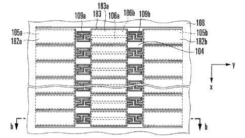
converting light into an electrical signal. Use of the optical
switch also makes it possible to switch the path without
demultiplexing multiplexed light into wavelengths. Such an
optical switch is used to, e.g., upon failure occurrence in a use
CA 02764403 2012-01-13
path, distribute a signal to another path and maintain a
communicable state.
[0004] In recent years, research and development of
wavelength selective switches is in progress, which demultiplex
multiplexed light into wavelengths and individually select the
paths of light of the respective wavelengths. These wavelength
selective switches also use micromirror devices.
[0005] A micromirror device (micromirror array) disclosed in
reference 1 will be explained below with reference to Figs. 29
and 30. The micromirror array includes a mirror substrate and an
electrode substrate facing it. The mirror substrate has a
plurality of movable structures acting as a mirror, and a support
member which rotationally supports the movable structures via
spring members such as torsion springs. For the electrode
substrate, a plurality of electrode portions corresponding to the
movable structures acting as a mirror are formed on a substrate
serving as a base.
[0006] Fig. 29 is a perspective view schematically showing
the arrangements of a mirror substrate and an electrode
substrate. Fig. 30 is a sectional view schematically showing the
arrangement of a micromirror device. Note that Figs. 29 and 30
partially illustrate a micromirror device which is mainly one
constituent unit of a micromirror array. A micromirror array is
formed by one- or two-dimensionally arraying the micromirror
devices shown in Figs. 29 and 30. Each micromirror device
includes a mirror substrate 200 having a mirror, and an electrode
- 2 -
CA 02764403 2012-01-13
substrate 300 having electrodes. The mirror substrate 200 and
the electrode substrate 300 are arranged in parallel to each
other.
[0007] The mirror substrate 200 includes a plate-shaped base
portion 210, a ring-shaped gimbal 220, and a disc-shaped mirror
230. The base portion 210 has an opening having an almost
circular shape viewed from above. The gimbal 220 is arranged in
the opening of the base portion 210 and connected to the base
portion 210 via a pair of connectors 211a and 211b. The gimbal
220 also has an opening having an almost circular shape viewed
from above. The mirror 230 is arranged in the opening of the
gimbal 220 and connected to the gimbal 220 via a pair of mirror
connectors 221a and 221b. A frame portion 240 is formed around
the base portion 210 to surround the gimbal 220 and the mirror
230. The frame portion 240 is fixed to the base portion 210 via
an insulating layer 250.
[0008] The connectors 211a and 211b are provided in the
notches of the gimbal 220. The connectors 211a and 211b are
formed from meander-shaped torsion springs and connect the base
portion 210 to the gimbal 220. The gimbal 220 thus connected to
the base portion 210 can rotate about a rotation axis (gimbal
rotation axis) which passes through the connectors 211a and 211b.
The mirror connectors 221a and 221b are provided in the notches
of the gimbal 220. The mirror connectors 221a and 221b are
formed from meander-shaped torsion springs and connect the gimbal
220 to the mirror 230. The mirror 230 thus connected to the
- 3 -
CA 02764403 2012-01-13
gimbal 220 can rotate about a rotation axis (mirror rotation
axis) which passes through the mirror connectors 221a and 221b.
Note that the gimbal rotation axis and the mirror rotation axis
are perpendicular to each other.
[0009] On the other hand, the electrode substrate 300
includes a plate-shaped base portion 310, a projecting portion
320 which projects from the upper surface of the base portion
310, and a pair of convex portions 360a and 360b which are formed
at the periphery of the projecting portion 320 to be juxtaposed
while sandwiching the projecting portion 320. The projecting
portion 320 includes a second terrace 322 having a truncated
pyramidal shape, a first terrace 321 having a truncated pyramidal
shape and formed on the upper surface of the second terrace 322,
and a pivot 330 having a truncated pyramidal shape and formed on
the upper surface of the first terrace 321. The pivot 330 is
arranged in correspondence with the central portion of the mirror
230.
[0010] Fan-shaped electrodes 340a, 340b, 340c, and 340d are
formed on the upper surface of the electrode substrate 300
including the outer surface of the projecting portion 320 so as
to be located in a circle concentric to the mirror 230 of the
opposite mirror substrate 200. Electrical interconnections 370
are formed inside the convex portions 360a and 360b at the
periphery of the projecting portion 320 on the electrode
substrate 300. The electrodes 340a to 340d are connected to the
electrical interconnections 370 via leads 341a to 341d. The
- 4 -
CA 02764403 2012-01-13
electrodes and the electrical interconnections are formed on an
insulating layer 311 which is formed on the surface of the
electrode substrate 300.
[0011] In the mirror substrate 200 and the electrode
substrate 300 which have the above-described arrangements, the
mirror 230 faces the corresponding electrodes 340a to 340d.
Additionally, the lower surface of the base portion 210 is bonded
to the upper surfaces of the convex portions 360a and 360b of the
base portion 310 via the insulating layer 311, thereby forming
the micromirror device shown in Fig. 30.
[0012] In this micromirror device, the mirror 230 is
grounded, and positive or negative voltages are applied to the
electrodes 340a to 340d to generate an asymmetrical potential
difference between them. This allows to attract the mirror 230
by an electrostatic attraction and make it rotate in an arbitrary
direction. When forming, e.g., a 1-input 2-output optical switch
using the micromirror device, the tilt angle of the mirror 230 is
controlled to irradiate the mirror 230 with an optical signal
from the input port and make the light reflected by the mirror
230 incident on one of the two output ports.
Disclosure of Invention
Problem to be Solved by the Invention
[0013] In the conventional micromirror device shown in Figs.
29 and 30, for example, two pairs of almost fixed points are
provided at the connection points between the mirror 230 and the
mirror connectors 221a and 221b and between the gimbal 220 and
- 5 -
CA 02764403 2012-01-13
the connectors 211a and 211b. The axes that connect the two
pairs of almost fixed points serve as the mirror rotation axis
and the gimbal rotation axis to make the mirror 230 rotate in two
different directions. Hence, when using the above-described
conventional micromirror device, adjacent mirrors need to be
spaced apart at a distance corresponding to the size of the
connectors that form the rotation axes.
[0014] To switch the paths of light of respective wavelengths
which are obtained by causing a grating or the like to
demultiplex a multiplexed optical signal in a uniaxial direction,
as in a wavelength selective switch, it is necessary to use a
micromirror array which is formed by one-dimensionally arraying
micromirror devices capable of rotating in two different
directions while reducing the interval between adjacent mirrors
to a predetermined value or less. If the interval between the
mirrors increases relative to the interval of the paths of
demultiplexed light of the respective wavelengths, light strikes
a region between the mirrors. This makes it impossible to guide
light of a wavelength concerned to an output port. For example,
to cause a wavelength selective switch to switch optical signals
demultiplexed by a grating and having a relatively narrow
wavelength interval, the central interval between the arrayed
mirrors is required to be as narrow as about 100 m. Depending
on required specifications about the passbands of optical
signals, the array-direction width of each mirror is sometimes
required to be 80% or more of the central interval of the
- 6 -
CA 02764403 2012-01-13
mirrors. In this case, the interval between the adjacent mirrors
is required to be 20 m or less.
[0015] Hence, in, e.g., a wavelength selective switch which
switches the paths of light of the respective wavelengths
demultiplexed using a grating or the like, the above-described
mirror's two-axis rotation operation needs to be performed in a
situation wherein the interval between the adjacent mirrors is 20
m or less. In the conventional micromirror device shown in
Figs. 29 and 30, however, the mirrors need to be spaced apart in
the direction of each rotation axis at a distance corresponding
to the size of the connectors. When the two-axis rotation
operation is enabled, it is impossible to meet the above-
described requirement of a narrow mirror interval.
[0016] The present invention has been made to solve the
above-described problem, and has as its object to enable the
mirror's two-axis rotation operation even in a situation wherein
the interval between adjacent mirrors is narrower.
Means of Solution to the Problem
[0017] According to the present invention, there is provided
a micromirror device comprising a reflecting portion and an
electrode portion facing the reflecting portion, the reflecting
portion comprising at least a first movable beam and a second
movable beam each having one end fixed and the other end
displaceable, the first movable beam and the second movable beam
being arranged in a line at a predetermined distance while the
other end of the first movable beam faces the other end of the
- 7 -
CA 02764403 2012-01-13
second movable beam, a mirror which is arrayed in a line with the
first movable beam and the second movable beam and rotationally
arranged between the first movable beam and the second movable
beam, and for example, a pair of a first flexible connector and a
second flexible connector each of which connects the other end of
a corresponding one of the first movable beam and the second
movable beam to the mirror, and the electrode portion comprising
at least a driving electrode for first movable beam which faces
the first movable beam at a predetermined distance, a driving
electrode for second movable beam which faces the second movable
beam at a predetermined distance, and mirror driving electrodes
which face the mirror at a predetermined distance. The mirror
rotates about two rotation axes by the displacement operation of
the first movable beam and the second movable beam.
[0018] According to the present invention, there is also
provided a micromirror array including a plurality of micromirror
devices arrayed, the micromirror device comprising a reflecting
portion and an electrode portion facing the reflecting portion,
the reflecting portion comprising at least a first movable beam
and a second movable beam each having one end fixed and the other
end displaceable, the first movable beam and the second movable
beam being arranged in a line at a predetermined distance while
the other end of the first movable beam faces the other end of
the second movable beam, a mirror which is arrayed in a line with
the first movable beam and the second movable beam and
rotationally arranged between the first movable beam and the
- 8 -
CA 02764403 2012-01-13
second movable beam, and a pair of a first connector and a second
connector each of which connects the other end of a corresponding
one of the first movable beam and the second movable beam to the
mirror, the electrode portion comprising at least a driving
electrode for first movable beam which faces the first movable
beam at a predetermined distance, a driving electrode for second
movable beam which faces the second movable beam at a
predetermined distance, and mirror driving electrodes which face
the mirror at a predetermined distance, and the micromirror
devices being arrayed along a direction perpendicular to an array
direction of the first movable beam and the second movable beam.
[0018.1] In accordance with one aspect of the present
invention, there is provided a micromirror device comprising a
reflecting portion and an electrode portion facing the reflecting
portion, the reflecting portion comprising at least: a first
movable beam and a second movable beam each having one end fixed
and the other end displaceable, the first movable beam and the
second movable beam being arranged in a line at a predetermined
distance while the other end of the first movable beam faces the
other end of the second movable beam; a mirror which is arrayed
in a line with the first movable beam and the second movable beam
and rotationally arranged between the first movable beam and the
second movable beam; and a pair of a first connector and a second
connector each of which connects the other end of a corresponding
one of the first movable beam and the second movable beam to the
mirror, and the electrode portion comprising at least: a driving
- 9 -
CA 02764403 2012-01-13
electrode for first movable beam which faces the first movable
beam at a predetermined distance; a driving electrode for second
movable beam which faces the second movable beam at a
predetermined distance; and mirror driving electrodes which face
the mirror at a predetermined distance; wherein each of the first
movable beam and the second movable beam includes a beam portion
on a side of the one end and a beam portion on a side of the
other end, and a width of the beam portion on the side of the one
end is different from a width of the beam portion on the side of
the other end.
[0018.2] In accordance with another aspect of the present
invention, there is provided a micromirror array including a
plurality of micromirror devices arrayed, the micromirror device
comprising a reflecting portion and an electrode portion facing
the reflecting portion, the reflecting portion comprising at
least: a first movable beam and a second movable beam each having
one end fixed and the other end displaceable, the first movable
beam and the second movable beam being arranged in a line at a
predetermined distance while the other end of the first movable
beam faces the other end of the second movable beam; a mirror
which is arrayed in a line with the first movable beam and the
second movable beam and rotationally arranged between the first
movable beam and the second movable beam; and a pair of a first
connector and a second connector each of which connects the other
end of a corresponding one of the first movable beam and the
second movable beam to the mirror, the electrode portion
- 10 -
CA 02764403 2012-01-13
comprising at least: a driving electrode for first movable beam
which faces the first movable beam at a predetermined distance; a
driving electrode for second movable beam which faces the second
movable beam at a predetermined distance; and mirror driving
electrodes which face the mirror at a predetermined distance, and
the micromirror devices being arrayed along a direction
perpendicular to an array direction of the first movable beam and
the second movable beam; wherein each of the first movable beam
and the second movable beam includes a beam portion on a side of
the one end and a beam portion on a side of the other end, and a
width of the beam portion on the side of the one end is different
from a width of the beam portion on the side of the other end.
Effect of the Invention
[0019] As described above, according to the present
invention, the first movable beam and the second movable beam
which are connected to the mirror via the pair of the first
connector and the second connector are provided. The
displacement operation of the first movable beam and the second
movable beam allows the mirror to rotate about the two rotation
axes. It is therefore possible to obtain an excellent effect of
enabling the two-axis rotation operation of the mirror even when
the interval between adjacent mirrors is narrower.
Brief Description of Drawings
[0020] Fig. 1A is a plan view showing an example of the
arrangement of micromirror devices (micromirror array) according
- 11 -
CA 02764403 2012-01-13
to the first embodiment of the present invention;
Fig. lB is a sectional view showing an example of the
arrangement of the micromirror device (micromirror array)
according to the first embodiment of the present invention;
Fig. 1C is a sectional view showing an example of the
arrangement of the micromirror device (micromirror array)
according to the first embodiment of the present invention;
Fig. 1D is a partially enlarged plan view showing an
example of the arrangement of the micromirror device (micromirror
array) according to the first embodiment of the present
invention;
Fig. 2 is a perspective view showing an example of the
arrangement of the micromirror devices (micromirror array)
according to the first embodiment of the present invention;
Figs. 3A and 3B are views for explaining a case in
which the projection destination of light reflected by a mirror
183 is switched among a plurality of ports arrayed at an
equidistance;
Fig. 4 is a plan view showing another example of the
arrangement of the connector of the micromirror device
(micromirror array) according to the first embodiment of the
present invention;
Fig. 5 is a plan view showing another example of the
arrangement of the micromirror devices (micromirror array)
according to the first embodiment of the present invention;
Fig. 6 is a plan view showing still another example of
- 12 -
CA 02764403 2012-01-13
the arrangement of the micromirror devices (micromirror array)
according to the first embodiment of the present invention;
Fig. 7A is a plan view showing still another example
of the arrangement of the micromirror devices (micromirror array)
according to the first embodiment of the present invention;
Fig. 7B is a partial sectional view showing still
another example of the arrangement of the micromirror device
(micromirror array) according to the first embodiment of the
present invention;
Figs. 8A and 8B are schematic sectional views for
explaining crosstalk;
Fig. 9A is a plan view showing still another example
of the arrangement of the micromirror devices (micromirror array)
according to the first embodiment of the present invention;
Fig. 9B is a partial sectional view showing still
another example of the arrangement of the micromirror device
(micromirror array) according to the first embodiment of the
present invention;
Fig. 9C is a plan view showing still another example
of the arrangement of the micromirror devices (micromirror array)
according to the first embodiment of the present invention;
Fig. 10A is a plan view showing still another example
of the arrangement of the micromirror devices (micromirror array)
according to the first embodiment of the present invention;
Fig. 10B is a partial sectional view showing still
another example of the arrangement of the micromirror device
- 13 -
CA 02764403 2012-01-13
(micromirror array) according to the first embodiment of the
present invention;
Fig. 10C is a plan view showing still another example
of the arrangement of the micromirror devices (micromirror array)
according to the first embodiment of the present invention;
Fig. 11A is a plan view showing another example of the
arrangement of the movable beam of the micromirror device
(micromirror array) according to the first embodiment of the
present invention;
Fig. 11B is a plan view showing the other example of
the arrangement of the movable beam of the micromirror device
(micromirror array) according to the first embodiment of the
present invention;
Fig. 12A is a plan view showing still another example
of the arrangement of the movable beam of the micromirror device
(micromirror array) according to the first embodiment of the
present invention;
Fig. 12B is a plan view showing the still other
example of the arrangement of the movable beam of the micromirror
device (micromirror array) according to the first embodiment of
the present invention;
Fig. 13A is a plan view showing an example of the
arrangement of micromirror devices (micromirror array) according
to the second embodiment of the present invention;
Fig. 13B is a sectional view showing an example of the
arrangement of the micromirror device (micromirror array)
- 14 -
CA 02764403 2012-01-13
according to the second embodiment of the present invention;
Fig. 13C is a sectional view showing an example of the
arrangement of the micromirror device (micromirror array)
according to the second embodiment of the present invention;
Fig. 14 is a perspective view showing an example of
the arrangement of the micromirror devices (micromirror array)
according to the second embodiment of the present invention;
Figs. 15A and 15B are schematic sectional views for
explaining crosstalk;
Figs. 16A and 16B are graphs for explaining a
crosstalk suppression effect;
Figs. 17A to 17C are sectional views showing other
examples of the arrangement of electrode walls of the micromirror
device (micromirror array) according to the second embodiment of
the present invention;
Fig. 18 is a sectional view for explaining the effect
of another electrode wall of the micromirror device (micromirror
array) according to the second embodiment of the present
invention;
Fig. 19A is a plan view showing another example of the
arrangement of the movable beam of the micromirror device
(micromirror array) according to the second embodiment of the
present invention;
Fig. 19B is a plan view showing still another example
of the arrangement of the movable beam of the micromirror device
(micromirror array) according to the second embodiment of the
- 15 -
CA 02764403 2012-01-13
present invention;
Fig. 20 is a perspective view showing an example of
the arrangement of micromirror devices (micromirror array)
according to the third embodiment of the present invention;
Fig. 21 is a sectional view showing an example of the
arrangement of the micromirror device (micromirror array)
according to the third embodiment of the present invention;
Fig. 22 is a sectional view showing an example of the
arrangement of the micromirror devices (micromirror array)
according to the third embodiment of the present invention;
Fig. 23 is a schematic sectional view for explaining
crosstalk;
Fig. 24 is a sectional view showing another example of
the arrangement of an upper inter-device electrode of the
micromirror device (micromirror array) according to the third
embodiment of the present invention;
Fig. 25 is a sectional view showing still another
example of the arrangement of the upper inter-device electrode of
the micromirror device (micromirror array) according to the third
embodiment of the present invention;
Fig. 26 is a schematic sectional view for explaining
an example of the arrangement of an inter-device electrode wall
of the micromirror device (micromirror array) according to the
third embodiment of the present invention;
Fig. 27A is a sectional view showing another example
of the arrangement of the micromirror device (micromirror array)
- 16 -
CA 02764403 2012-01-13
according to the third embodiment of the present invention;
Fig. 27B is a plan view showing another example of the
arrangement of the micromirror device (micromirror array)
according to the third embodiment of the present invention;
Fig. 28A is a sectional view showing another example
of the arrangement of the micromirror device (micromirror array)
according to the third embodiment of the present invention;
Fig. 28B is a plan view showing another example of the
arrangement of the micromirror device (micromirror array)
according to the third embodiment of the present invention;
Fig. 29 is a perspective view showing the arrangement
of a conventional micromirror device (micromirror array);
Fig. 30 is a sectional view showing the arrangement of
the conventional micromirror device (micromirror array); and
Fig. 31 is a view for explaining a port switching
operation.
Best Mode for Carrying Out the Invention
[0021] The embodiments of the present invention will now be
described with reference to the accompanying drawings.
[0022] [First Embodiment]
The first embodiment of the present invention will be
described first with reference to Figs. lA to 1D. Fig. lA is a
plan view showing an example of the arrangement of micromirror
devices according to the first embodiment. Figs. 1B and 1C are
sectional views showing an example of the arrangement of the
micromirror device according to the first embodiment. Fig. 1D is
- 17 -
CA 02764403 2012-01-13
a partially enlarged plan view showing an example of the
arrangement of the micromirror device according to the first
embodiment. Fig. 1A illustrates a micromirror array formed by
arraying a plurality of micromirror devices in the vertical
direction (x direction) of the drawing surface.
[0023] A micromirror device according to the first embodiment
includes, e.g., an electrode substrate 101 and a mirror substrate
108 facing it. A support structure 107 provided to surround a
micromirror array region including the plurality of micromirror
devices fixes the mirror substrate 108 above the electrode
substrate 101 at a predetermined distance. The electrode
substrate 101 and the mirror substrate 108 are arranged in
parallel to each other.
[0024] An electrical interconnection layer including
electrical interconnections 102 and 103, and an interlayer
dielectric film 104 covering the electrical interconnection layer
are formed on the electrode substrate 101 made of single-crystal
silicon. In correspondence with each micromirror device, movable
beam driving electrodes 105a and 105b and mirror driving
electrodes 106a and 106b are provided on the interlayer
dielectric film 104 on the electrode substrate 101. The movable
beam driving electrodes 105a and 105b and mirror driving
electrodes 106a and 106b constitute one electrode portion (one
electrode portion group).
[0025] The movable beam driving electrodes 105a and 105b are
connected to some of the electrical interconnections 102 via
- 18 -
CA 02764403 2012-01-13
through electrodes 110 which extend through the interlayer
dielectric film 104. The mirror driving electrodes 106a and 106b
are connected some of the electrical interconnections 103 via
through electrodes 111 which extend through the interlayer
dielectric film 104. Note that in the above description, the
electrical interconnections are arranged while ensuring
interlayer isolation by the interlayer dielectric film 104.
However, the present invention is not limited to this. The
electrical interconnections may be provided on the electrode
formation surfaces.
[0026] The mirror substrate 108 includes a frame portion 181
having an opening to expose the micromirror array region. The
frame portion 181 is connected to the support structure 107.
Movable beams 182a and 182b each having one end fixed to the
frame portion 181 are provided inside the frame portion 181 of
the mirror substrate 108. One end of each of the movable beams
182a and 182b is fixed to a corresponding one of the two opposite
internal sides of the frame portion 181. Hence, the movable
beams 182a and 182b are aligned at a predetermined distance on
the same line in the direction in which the two sides face each
other. That is, the movable beams 182a and 182b each having one
end fixed and the other end facing that of the counterpart are
arranged in line at a predetermined distance. In the example
shown in Fig. 1A, the movable beams 182a and 182b are aligned on
a line parallel to the y-axis direction. Additionally, each of
the movable beams 182a and 182b has the other end displaceable in
- 19 -
CA 02764403 2012-01-13
the normal line direction of the mirror substrate 108 and
therefore has a cantilever structure.
[0027] A mirror 183 is arranged between the movable beams
182a and 182b and connected to them via a pair of flexible
connectors 109a and 109b. The mirror 183 is aligned with the
movable beams 182a and 182b and rotationally arranged between
them. The connectors 109a and 109b connect the other end of each
of the movable beams 182a and 182b to the mirror 183. The
movable beam 182a, the mirror 183, and the movable beam 182b are
aligned in this order on the same line in the direction in which
the two sides connected to the movable beams 182a and 182b face
each other. The movable beam 182a, the mirror 183, the movable
beam 182b, and the pair of connectors 109a and 109b form one
reflecting portion (one reflecting portion group).
[0028] In the example shown in Figs. 1A, 1B, and 1C, the
movable beam 182a, the mirror 183, and the movable beam 182b are
aligned on a line parallel to the y-axis direction. The mirror
183 can rotate about a first rotation axis which passes through
the pair of connectors 109a and 109b. In the example shown in
Figs. 1A, 1B, and 1C, the mirror 183 can rotate about the first
rotation axis parallel to the y-axis direction. In Fig. 1A, a
plurality of micromirror devices are arranged along a direction
perpendicular to the alignment (array) direction of the movable
beam 182a, the mirror 183, and the movable beam 182b, thereby
forming a micromirror array. Note that a reflecting film 183a
of, e.g., gold or aluminum is formed on the surface of the mirror
- 20 -
CA 02764403 2012-01-13
183 to reflect, for example, light in the infrared region.
[0029] The above-described movable beam driving electrodes
105a and 105b and the set of the mirror driving electrodes 106a
and 106b, the movable beam 182a, the mirror 183, the movable beam
182b, which are paired with the electrodes, and the pair of
connectors 109a and 109b form one micromirror device. In one
micromirror device, the movable beam driving electrode 105a and
the movable beam 182a are arranged while facing each other in the
normal line direction (z-axis direction) of the electrode
substrate 101 (mirror substrate 108), and so are the movable beam
driving electrode 105b and the movable beam 182b, and the set of
mirror driving electrodes 106a and 106b and the mirror 183.
[0030] Driving voltages (driving signals) to drive the
movable beams 182a and 182b are applied to the movable beam
driving electrodes 105a and 105b via the electrical
interconnections 102. Driving voltages to drive the mirror 183
are applied to the mirror driving electrodes 106a and 106b via
the electrical interconnections 103. Note that the electrical
interconnection 102 connected to the movable beam driving
electrode 105a is different from the electrical interconnection
102 connected to the movable beam driving electrode 105b,
although they are simply illustrated in the drawings. Similarly,
the electrical interconnection 103 connected to the mirror
driving electrode 106a is different from the electrical
interconnection 103 connected to the mirror driving electrode
106b. This enables to apply different arbitrary driving
- 21 -
CA 02764403 2012-01-13
voltages. Note that the movable beam 182a, the mirror 183, the
movable beam 182b, and the pair of connectors 109a and 109b are
set at an equipotential. The equipotential is, for example, the
ground potential.
[0031] The micromirror device according to the above-
described first embodiment is formed by bonding the electrode
substrate 101 and the mirror substrate 108 via the support
structure 107. The mirror substrate 108 can be formed from,
e.g., an SO1 (Silicon On Insulator) substrate. The SOI substrate
has a thin silicon layer (SOI layer) on a buried insulating layer
formed on a thick silicon substrate portion. Plate-shaped
structures such as the frame portion 181, the movable beams 182a
and 182b, the connectors 109a and 109b, and the mirror 183 can be
formed by processing the SOI layer. After processing these
structures, the substrate portion, the buried insulating layer,
and the like are removed. The reflecting film 183a is formed by
depositing a desired metal by, e.g., sputtering or vapor
deposition.
[0032] On the other hand, the electrode substrate 101 can be
formed using a well-known method of manufacturing a semiconductor
device such as an LSI integrated circuit. Alternatively, an
electrode substrate having the support structure 107 may be
formed by etching, in an alkali solution such as a potassium
hydroxide solution, a single-crystal silicon substrate having a
(100) plane as a major surface in terms of crystal orientation,
and forming a concave portion having a predetermined depth in the
- 22 -
CA 02764403 2012-01-13
silicon substrate. As is well known, the etching rate of the
(111) plane of single-crystal silicon in alkali is considerably
lower than that of the (100) or (110) plane. Use of this
phenomenon makes it possible to form a support structure having a
truncated pyramidal shape.
[0033] Note that a separately prepared support structure may
be used. For example, a support structure formed by solder bumps
or plating may be used. Alternatively, an integrated circuit
including a plurality of elements connected to the electrical
interconnections 102 and 103 may be provided on the electrode
substrate 101 to form a control circuit for controlling driving
voltages to be applied to the electrodes. Otherwise, the mirror
portion and the electrode portion may integrally be built up by
surface micromachining.
[0034] The operation of the micromirror device will be
described next. First, a predetermined driving voltage is
applied to the movable beam driving electrode 105b to generate an
electrostatic attraction and thus attract the movable beam 182b
toward the electrode substrate 101. The movable beam 182b bends
(deforms) using its end supported by the frame portion 181 as a
fulcrum so that the other end of the movable beam 182b displaces
toward the electrode substrate 101, as shown in Fig. 1C.
Consequently, the mirror 183 is attracted toward the electrode
substrate 101 on the side of the connector 109b using the
connector 109a as a fulcrum. The mirror 183 is not parallel to
the electrode substrate 101 any longer but tilts in the y-axis
- 23 -
CA 02764403 2012-01-13
direction. Note that Fig. 1B illustrates the initial state
before voltage application to the electrodes.
[0035] In the state shown in Fig. 1C, the mirror 183 rotates
about the second rotation axis which passes through the central
portion of the mirror 183 and is parallel to the micromirror
device array direction (x-axis direction). The mirror can
perform this rotation operation even by applying a predetermined
driving voltage to the movable beam driving electrode 105a to
attract the other end of the movable beam 182a toward the
electrode substrate 101 in the same way as described above. In
this case, the mirror 183 rotates about the second rotation axis
in a direction opposite to that in the above-described case. A
case will be explained in which, for example, the projection
destination of light reflected by the mirror 183 is switched
among a plurality of ports arrayed at an equidistance, as shown
in Fig. 31. In this case, the driving voltage applied to the
movable beam driving electrode 105a is changed as shown in Fig.
3A, thereby controlling the rotation angle of the pivot operation
of the mirror 183 about the second rotation axis, as shown in the
perspective view of Fig. 3B.
[0036] The rotation angle of the mirror 183 about the second
rotation axis is decided based on the relationship between the y-
axis direction length between the portions of the connectors 109a
and 109b connected to the two ends of the mirror 183 and the
subsidence amount of the central portion of the connector 109a or
109b when the movable beam 182a or 182b is attracted toward the
- 24 -
CA 02764403 2012-01-13
electrode substrate 101. For example, when the length between
the central portions of the connectors 109a and 109b is 500 m,
and the subsidence amount is 13 m, a rotation angle 8 of the
mirror 183 is 8 = tan - 1(13/500) 1.5 . The subsidence amount
is decided by the balance between an electrostatic attraction
generated upon driving voltage application to the movable beam
driving electrode 105a or 105b and a repulsive force defined by
the z-axis direction spring constant of the movable beam 182a or
182b. To more largely rotate the mirror 183 by a less
electrostatic attraction, it is effective to increase the areas
of the movable beam driving electrodes and the movable beams. If
the width (x-axis direction) is constant, it is effective to
increase the length (y-axis direction). For example, the ratio
of the length between the central portions of the pair of
connectors 109a and 109b to the length of the movable beam 182a
or 182b is preferably approximately 2 : 1.
[0037] The above-described rotation about the second rotation
axis is done while moving the second rotation axis in the z-axis
direction. However, displacing the movable beams 182a and 182b
to different sides in the z-axis direction allows the mirror 183
to rotate about the second rotation axis without moving it. For
example, predetermined bias voltages are applied to the movable
beam driving electrodes 105a and 105b, and then, the driving
voltages applied to them are controlled, thereby displacing the
movable beams 182a and 182b to different sides in the z-axis
direction.
- 25 -
CA 02764403 2012-01-13
[0038] Controlling voltages applied to the mirror driving
electrodes 106a and 106b enables the mirror 183 to rotate about
the first rotation axis which passes through the pair of
connectors 109a and 109b, as shown in the perspective view of
Fig. 2. For example, a higher voltage is applied to the mirror
driving electrode 106b relative to the mirror driving electrode
106a. This allows control to tilt the mirror 183 toward the
mirror driving electrode 106b about the first rotation axis. The
conventional micromirror device is designed as an element using
connectors as almost fixed ends. However, the micromirror device
according to the first embodiment actively moves the pair of
connectors 109a and 109b, thereby realizing two-axis rotation via
them. Note that in the above description, the pair of mirror
driving electrodes 106a and 106b are provided to be linearly
symmetric with the first rotation axis. However, the present
invention is not limited to this. It is also possible to make
the mirror 183 rotate using only one mirror driving electrode.
Hence, one mirror driving electrode suffices.
[0039] Note that an electrostatic attraction drives the
mirror 183. The deformed state, i.e., the rotation angle of the
mirror is decided based on parameters including the distance
between the reflecting portion and the electrode portion, the
dielectric constant of a gas (air) that exists between them, the
voltage applied across the reflecting portion and the electrode
portion, and the areas and rigidities of structures such as the
mirror and the movable beams. Hence, designing a micromirror
- 26 -
CA 02764403 2012-01-13
device handles deciding the above-described parameters to meet
required specifications. The materials, sizes, and shapes of the
structures are appropriately decided in accordance with the
required specifications. Especially, as for the shape of the
connectors 109a and 109b, a meander-shaped structure shown in
Fig. 4 is applicable in some cases. The connectors 109a and 109b
may have another shape. For example, a connector which has, at
the long portion (x-axis direction) of the meander-shaped
structure, a plurality of bending portions with projections and
recesses alternately arranged in a direction different from the
running direction may be used (reference 2: Japanese Patent No.
3831346).
[0040] The connectors 109a and 109b will be described next.
For example, the connector 109a has an almost rectangular section
perpendicular to the x-axis direction or the y-axis direction.
The connector 109a has a nearly H-like planar shape with almost
rectangular parts formed symmetrically with respect to the
rotation axis, as shown in the plan view of Fig. 1D. The
connector 109a includes 15 parts 191a, 192a, 193a, 194a, 195a,
196a, 197a, 198, 191b, 192b, 193b, 194b, 195b, 196b, and 197b.
The part 191a is connected to the movable beam 182a, and the part
191b is connected to one end of the mirror 183, thereby
rotationally connecting the mirror 183 to the movable beam 182a.
[0041] Note that the direction in which the connector 109a
connects one connection point to the other connection points will
be referred to as "rotation axis direction" or "y-axis
- 27 -
CA 02764403 2012-01-13
direction". The widthwise direction of the connector 109a, i.e.,
a direction perpendicular to the y-axis direction in a plane
including the connector 109a will be referred to as "x-axis
direction". The thickness direction of the connector 109a, i.e.,
a direction perpendicular to the y- and x-axis directions will be
referred to as "z-axis direction". The direction in which the
mirror 183 connected to the connector 109a rotates, i.e., a
direction about the y-axis will be referred to as "rotation
direction" or "R direction".
[0042] The planar shape of the connector 109a will be
described in more detail. The connector 109a has a nearly H-like
planar shape by continuously connecting the parts 191a to 197a,
191b to 197b, and 198, as shown in Fig. 1D. Each of the parts
191a to 191b has an almost rectangular beam-like planar shape and
is arranged in the following manner. Note that the distance of
each part indicates the length of a corresponding line segment of
a line that expresses the connector 109a, i.e., the length of the
center line of each part along the part connection direction.
[0043] The part 191a is formed to run by a distance Ll in the
positive y-axis direction from one end connected to the movable
beam 182a. The part 192a is formed to run by a distance L2 in
the positive x-axis direction from one end connected to the other
end of the part 191a. The part 193a is formed to run by a
distance L3 (L1 > L3) in the negative y-axis direction from one
end connected to the other end of the part 192a. The part 194a
is formed to run by the distance L2 in the positive x-axis
- 28 -
CA 02764403 2012-01-13
direction from one end connected to the other end of the part
193a. The part 195a is formed to run by a distance L4 (L4 > L3)
in the positive y-axis direction from one end connected to the
other end of the part 194a.
[0044] The part 196a is formed to run by the distance L2 in
the negative x-axis direction from one end connected to the other
end of the part 195a. The part 197a is formed to run by a
distance L5 (L4 > L5 > L3, (L4 - L3) > L5) in the negative y-axis
direction from one end connected to the other end of the part
196a. The part 198 is formed to run by a distance L6 (L6 2L2)
in the negative x-axis direction from one end connected to the
other end of the part 197a. The part 197b is formed to run by
the distance L5 in the negative y-axis direction from one end
connected to the other end of the part 198. The part 196b is
formed to run by the distance L2 in the negative x-axis direction
from one end connected to the other end of the part 197b.
[0045] The part 195b is formed to run by the distance L4 in
the positive y-axis direction from one end connected to the part
196b. The part 194b is formed to run by the distance L2 in the
positive x-axis direction from one end connected to the other end
of the part 195b. The part 193b is formed to run by the distance
L3 in the negative y-axis direction from one end connected to the
other end of the part 194b. The part 192b is formed to run by
the distance L2 in the positive x-axis direction from one end
connected to the other end of the part 193b. The part 191b is
formed to run by the distance L1 in the positive y-axis direction
- 29 -
CA 02764403 2012-01-13
from one end connected to the other end of the part 192b.
[0046] The total length of the parts 191a, 193a, 195a, 197a,
197b, 195b, 193b, and 191b of the connector 109a formed in the y-
axis direction is longer than the interval between the movable
beam 182a and the mirror 183 (the total length of the connector
109a) in a no-load state and also longer than the total length of
the parts 192a, 194a, 196a, 198, 196b, 194b, and 192b formed in
the x-axis direction. The total length indicates a length
obtained by connecting the parts in a line along the longitudinal
direction, i.e., the y- or x-axis direction. Note that the parts
192a and 194a and the parts 194b and 192b are formed to have the
same length. However, they may be formed in different lengths.
Similarly, the parts 191a and 191b may also be formed in
different lengths.
[0047] The lengths of the parts 191a to 191b can freely be
set as needed by, e.g., forming all parts in different lengths
and shifting the axis of the part 191a from that of the part 191b
as far as the parts formed in parallel are spaced apart from each
other. Hence, at least the parts 191a and 197b, the parts 192a
and 198, the parts 197a and 191b, and the parts 198 and 192b are
formed to be spaced apart from each other.
[0048] Examples of parameters that decide the characteristics
such as the spring constant of the connector 109a having the
above-described shape are the total length and width of the
connector 109a, the total length of the parts formed in parallel
to the y-axis direction, the total length of the parts formed in
- 30 -
CA 02764403 2012-01-13
parallel to the x-axis direction, and the thickness of the
connector 109a. The parameters also include the interval between
the parts parallel to the y-axis and the ratio of the length of a
part (part 195a or 195b) parallel to the y-axis direction with
respect to the total length.
[0049] According to the connectors 109a and 109b having the
above-described nearly H-like planar shape, when setting a small
spring constant in the R direction, the spring constant in each
axial direction can be made larger as compared to a connector
having a meander shape. This is because the spring constant of
the connector in the R direction greatly depends on the length of
the parts formed in the rotation axis direction, i.e., the y-axis
direction. The parts formed in the y-axis direction correspond
to, e.g., the parts 191a, 193a, 195a, 197a, 197b, 195b, 193b, and
191b in Fig. 1D.
[0050] In a microstructure such as a MEMS, the value of the
spring constant in the R direction results more largely from the
torsion of the connector than from its bending. For this reason,
a connector which is assumed to bend to make the mirror rotate,
like the conventional connector having a meander shape, cannot
make the spring constant in the R direction small while keeping a
large spring constant in each axial direction by extending the
folded portions and the like. Additionally, the y-axis direction
length of the conventional connector having a meander shape is
limited, i.e., cannot exceed the length of the entire connector.
It is therefore difficult to freely set the spring constant in
- 31 -
CA 02764403 2012-01-13
the R direction within a wide range as needed.
[0051] To the contrary, the almost H-shaped connectors 109a
and 109b which turn a plurality of number of times in the y-axis
direction readily twist about the y-axis, i.e., have a small
spring constant in the R direction because the parts in the y-
axis direction are long. This makes it possible to freely set
the spring constant in the R direction within a wide range as
needed without making the spring constants in the x-, y-, and t-
axis directions smaller than in the connector having a meander
shape. Especially, it is possible to set a larger spring
constant in each axial direction and freely set the spring
constant in the R direction within a wide range as needed by
making the total length of the parts having axes parallel to the
y-axis direction of the connectors 109a and 109b larger than the
total length of the parts having axes parallel to the x-axis
direction.
[0052] The connectors 109a and 109b having a nearly H-like
planar shape can include more parts parallel to the y-axis
direction within the limited space in the x-axis direction and
therefore cause torsions about more axes. This enables to make
the spring constant in the R direction smaller. Note that use of
the connectors having a nearly H-like planar shape facilitates
control of the spring constant in the R direction. However, a
torsion spring having a meander shape may be used as a connector
409, as shown in Fig. 4, as a matter of course.
[0053] Note that in the above description, a plurality of
- 32 -
CA 02764403 2012-01-13
micromirror devices are arrayed at an equidistance. However, the
present invention is not limited to this. For example, if each
optical signal as the path switching target is demultiplexed at a
predetermined frequency interval, the micromirror devices
(mirrors 183) have not a predetermined interval but intervals
calculated by formulas related to the frequencies of the optical
signals. To the contrary, if optical signals as the path
switching target are demultiplexed at a predetermined wavelength
interval, the micromirror devices (mirrors 183) generally have a
predetermined interval.
[0054] The width (x-axis direction) and length (y-axis
direction) of each mirror 183 and the x-axis direction array
interval of the mirrors 183 are decided based on the wavelength
interval of optical signals as the path switching target, the
passband or transmission band of each optical signal, and the
specifications and design of the beam of each optical signal.
For example, to set the frequency interval of optical signals to
100 GHz and the passband (0.5 dB bandwidth) to 60 GHz when the
beam radius on the mirror 183 is 20 m, the x-axis direction
array interval of the mirrors 183 is set to 100 gm, and the width
is set to 85 gm.
[0055] In the above description, the mirror 183 is
rectangular when viewed from above. However, the present
invention is not limited to this. For example, the opposite
sides (side surfaces) of the mirror 183 in the micromirror device
array direction may be projected toward the adjacent micromirror
- 33 -
CA 02764403 2012-01-13
devices to form a mirror 583, as shown in the plan view of Fig.
5. In other words, the planar shape of the mirror 583 narrows
toward the connectors 109a and 109b. The mirror 583 is hexagonal
in the example shown in Fig. 5.
[0056] This makes it possible to reduce the narrow region
between adjacent mirrors and easily suppress locking of the
mirrors without causing demultiplexed light of the respective
wavelengths to strike the region between the mirrors. The
demultiplexed light of each wavelength is a circular or elliptic
beam. Hence, the above-described mirror shape can decrease beam
loss caused by vignetting between the adjacent mirrors when
reflecting a beam at the center of the mirror. In addition,
since the distance between the adjacent mirrors is minimized
almost at one point, the structure including the mirrors spaced
apart from each other can easily be formed in the manufacture.
[0057] Also usable is a mirror 683 having an elliptic planar
shape with a major axis being arranged on the first rotation axis
that passes through the pair of connectors 109a and 109b, as
shown in the plan view of Fig. 6. The elliptic shape also easily
suppresses locking of the mirrors, as described above.
Additionally, the elliptic shape without angles can suppress
contact between the rotating mirror and the electrode portion,
resulting in a wider rotation range.
[0058] In actual use, if an excess voltage is applied to a
driving electrode to generate an electrostatic attraction
(driving force) larger than the restoring force of the movable
- 34 -
CA 02764403 2012-01-13
beam or the connector during the above-described rotate about the
first and second rotation axes, the distal end of the movable
beam or the mirror on the connector side comes into contact
(collision) with the driving electrode. That is, a pull-in
phenomenon occurs. For example, such a pull-in phenomenon
(contact) may fuse and stick the distal end of the mirror to the
electrode or stick the movable beam and the electrode. This
disables the optical signal switching operation.
[0059] To avoid the above-described problem, for example, as
shown in Figs. 7A and 7B, movable beam extending portions 701 are
provided for the movable beams 182a and 182b on the sides of the
connectors 109a and 109b so as to run and surround the
connectors. In addition, mirror extending portions 702 are
provided for the mirror 183 on the sides of the connectors 109a
and 109b so as to run and surround the connectors. Furthermore,
support portions 703 are provided on the electrode substrate 101
(interlayer dielectric film 104). The support portions 703 are
formed to be higher than the movable beam driving electrodes 105a
and 105b and the mirror driving electrodes 106a and 106b.
[0060] In this case, for example, even when the movable beam
182a receives a large electrostatic attraction and is attracted
toward the electrode substrate 101, the movable beam extending
portions 701 come into contact with the support portion 703,
thereby preventing the movable beam 182a from coming into contact
with the movable beam driving electrode 105a. This avoids the
above-described problem of fusion or locking. Note that the
- 35 -
CA 02764403 2012-01-13
potential of the use portion 703 is preferably the same as that
of the mirror 183 and the movable beams 182a and 182b. For
example, the potential is preferably the ground potential. The
extending portions may be provided on one of the movable beam and
the mirror.
[0061] Crosstalk generated when the mirror driving electrodes
106a and 106b drive the mirror 183 will be explained next. As
described above, the micromirror devices are arrayed at a narrow
interval. For this reason, an electrostatic attraction generated
by the mirror driving electrode 106b of a given micromirror
device affects not only the mirror 183 of the micromirror device
of influence but also the mirror 183 of an adjacent micromirror
device, as shown in the sectional view of Fig. 8A. That is,
electrical interference (crosstalk) may occur between the
adjacent mirrors 183.
[0062] To solve the above problem, inter-device electrodes
801 set at the same potential (equipotential) as that of the
mirrors 183 are provided between the mirror driving electrodes
106b and 106a of adjacent micromirror devices, as shown in the
sectional view of Fig. 8B. The inter-device electrode 801
reduces the influence of crosstalk of the mirror driving
electrodes 106a and 106b on the mirrors 183 of adjacent
micromirror devices.
[0063] An example of formation of the inter-device electrode
to reduce the above-described influence of the crosstalk will be
described next. For example, as shown in Figs. 9A, 9B, and 9C,
- 36 -
CA 02764403 2012-01-13
an inter-device electrode 904 is formed to surround the pair of
mirror driving electrodes 106a and 106b of one micromirror
device. When forming the inter-device electrode 904 in the
above-described way, support portions 903 made of a conductive
material such as a metal are connected to the inter-device
electrode 904. This prevents charge accumulation in the support
portions 903. Note that Fig. 9A is a plan view showing a portion
where three micromirror devices are arrayed. Fig. 9B is a
partial sectional view. Fig. 9C is a plan view showing a state
in which the electrodes are formed in a region corresponding to
almost one micromirror device.
[0064] Alternatively, as shown in Figs. 10A, 10B, and 10C,
out of the opposite sides of a micromirror device which are
parallel when viewed from above, the outer sides may be shortened
to obtain trapezoidal shapes. Mirror driving electrodes 1006a
and 1006b may be formed into the trapezoidal shapes, and an
inter-device electrode 1004 may be formed conforming to the
electrode shape. In the example shown in Figs. 10A, 10B, and
10C, the mirror driving electrodes 1006a and 1006b have an
isosceles trapezoidal shape when viewed from above. Note that
the mirror driving electrodes 1006a and 1006b need not always
have the trapezoidal shape. It is only necessary to decrease the
length in the first rotation axis direction outward (toward the
adjacent micromirror devices) in the formation region of one
micromirror device so that the inter-device electrode 1004 can
enter more inward.
- 37 -
CA 02764403 2012-01-13
[0065] The mirror driving electrodes 1006a and 1006b having
rounded corners on the outer sides of the micromirror device
formation region (the sides of the adjacent micromirror devices)
allow the inter-device electrode 1004 to further enter toward the
mirror 183. Hence, support portions 1003 which further enter
toward the mirror 183 can be formed. It is consequently possible
to bring an end of the mirror 183 attracted toward the electrode
substrate 101 into contact with the support portion 1003 without
forming extending portions of the mirror 183. This solves the
above-described problem of locking without forming extending
portions of the mirror 183. Note that Fig. 1OA is a plan view
showing a portion where three micromirror devices are arrayed.
Fig. 10B is a partial sectional view. Fig. 1OC is a plan view
showing a state in which the electrodes are formed in a region
corresponding to almost one micromirror device.
[0066] A movable beam in another form will be described next.
For example, the movable beam 182a may have hole portions 1101,
as shown in the plan view of Fig. 11A and the sectional view of
Fig. 11B. Forming the hole portions 1101 enables to make the
spring constant of the movable beam 182a smaller in the region
having the hole portions 1101. When the spring constant is
smaller, the same deformation amount (displacement amount) of the
movable beam 182a can be obtained at a lower driving voltage as
compared to a structure without hole portions. Note that this
also applies to the movable beam 182b shown in Figs. 1A, 1B, and
1C.
- 38 -
CA 02764403 2012-01-13
[0067] Alternatively, a movable beam 1200a which is narrower
on the side fixed to the mirror substrate 108, as shown in Figs.
12A and 12B, may be used. The movable beam 1200a includes a beam
portion 1201a narrower on the fixed end side, and a beam portion
1202a between the narrow beam portion 1201a and the connector
109a. Referring to Fig. 12A, a movable beam driving electrode
1205a is provided in correspondence with the region of the beam
portion 1202a. Since the movable beam is narrower on the fixed
end side, the spring constant is small. This allows to ensure
the same deformation amount (displacement amount) of the movable
beam 1200a at a lower driving voltage as compared to a structure
without a narrow portion. It is therefore possible to obtain the
same deformation amount using the movable beam driving electrode
1205a having a small area. Otherwise, a movable beam driving
electrode 1215a corresponding to the entire region of the movable
beam 1200a may be provided, as shown in Fig. 12B. In this case,
the same deformation amount can be obtained at a lower driving
voltage. Note that the above description also applies to the
other movable beam facing the movable beam 1200a via a mirror.
[0068] [Second Embodiment]
The second embodiment of the present invention will be
described next with reference to Figs. 13A to 13C and 14.
Fig. 13A is a plan view showing an example of the arrangement of
micromirror devices according to the second embodiment.
Figs. 13B and 13C are sectional views showing an example of the
arrangement of the micromirror device according to the second
- 39 -
CA 02764403 2012-01-13
embodiment. Fig. 13A illustrates a micromirror array formed by
arraying a plurality of micromirror devices in the vertical
direction (x direction) of the drawing surface.
[0069] As the characteristic feature of the micromirror
device of the second embodiment, movable beam driving electrodes
105a and 105b have wall electrodes 115a and 115b, respectively.
Two wall electrodes 115a are arranged spaced-apart through at
least the region where a movable beam 184a displaces. Similarly,
two wall electrodes 115b are arranged to spaced-apart through at
least the region where a movable beam 184b displaces. The wall
electrodes 115a are electrically connected to the movable beam
driving electrode 105a. The wall electrodes 115b are
electrically connected to the movable beam driving electrode
105b. Note that the wall electrodes 115a and 115b need not be in
direct contact with the movable beam driving electrodes 105a and
105b. For example, they may be connected electrically via an
electrical interconnection layer under an interlayer dielectric
film 104.
[0070] The movable beam 184a facing each movable beam driving
electrode 105a has a width in such a range that enables
displacement toward the movable beam driving electrode 105a in
the region which is surrounded by the wall electrodes 115a.
Similarly, the movable beam 184b facing each movable beam driving
electrode 105b has a width in such a range that enables
displacement toward the movable beam driving electrode 105b in
the region which is surrounded by the wall electrodes 115b.
- 40 -
CA 02764403 2012-01-13
Hence, the movable beams 184a and 184b are formed to be narrower
than, e.g., a mirror 183.
[0071] Note that the remaining components are the same as in
the above-described first embodiment.
[0072] In the second embodiment, for example, the two wall
electrodes 115a are connected to the two side portions of the
movable beam driving electrode 105a in the direction (y-axis
direction) in which the movable beam 184a, the mirror 183, and
the movable beam 184b are arrayed. The wall electrodes 115a run
in the y-axis direction. Hence, on a section in the micromirror
device array direction, the movable beam driving electrode 105a
and the two wall electrodes 115a form a U shape open toward the
movable beam 184a. The movable beam 184a which is attracted upon
applying a predetermined driving voltage to the movable beam
driving electrode 105a enters between the two wall electrodes
115a. These also apply to the region of the movable beam driving
electrode 105b.
[0073] The operation of the second embodiment is the same as
in the above-described embodiment, as will be explained below.
First, a predetermined driving voltage is applied to the movable
beam driving electrode 105b to generate an electrostatic
attraction and thus attract the movable beam 184b toward an
electrode substrate 101. The movable beam 184b deforms using its
end supported by a frame portion 181 as a fulcrum so that the
other end of the movable beam 184b displaces toward the electrode
substrate 101, as shown in Fig. 13C. Consequently, the mirror
- 41 -
CA 02764403 2012-01-13
183 is attracted toward the electrode substrate 101 on the side
of a connector 109b using a connector 109a as a fulcrum. The
mirror 183 is not parallel to the electrode substrate 101 any
longer but tilts in the y-axis direction. Note that Fig. 13B
illustrates the initial state before voltage application to the
electrodes.
[0074] In the state shown in Fig. 13C, the mirror 183 rotates
about the second rotation axis which passes through the central
portion of the mirror 183 and is parallel to the micromirror
device array direction (x-axis direction). The above-described
rotation about the second rotation axis is done while moving the
second rotation axis in the z-axis direction. However,
displacing the movable beams 184a and 184b to different sides in
the z-axis direction allows the mirror 183 to rotate about the
second rotation axis without moving it. For example,
predetermined bias voltages are applied to the movable beam
driving electrodes 105a and 105b, and then, the driving voltages
applied to them are controlled, thereby displacing the movable
beams 184a and 184b to different sides in the z-axis direction.
[0075] Controlling voltages applied to mirror driving
electrodes 106a and 106b enables the mirror 183 to rotate about
the first rotation axis which passes through the pair of
connectors 109a and 109b, as shown in the perspective view of
Fig. 14. For example, a higher voltage is applied to the mirror
driving electrode 106b relative to the mirror driving electrode
106a. This allows control to tilt the mirror 183 toward the
- 42 -
CA 02764403 2012-01-13
mirror driving electrode 106b about the first rotation axis.
[0076] As described above, in the second embodiment as well,
the two-axis rotation operation of the mirror 183 is possible, as
in the above-described first embodiment. Additionally, in the
second embodiment, the wall electrodes 115a and 115b suppress
crosstalk to micromirror devices arranged adjacent, as will be
explained below.
[0077] The wall electrodes 115a and 115b will be described
below in more detail. Each micromirror device is arranged at a
narrow interval with respect to adjacent micromirror devices.
For this reason, if the movable beam driving electrode 105a is a
simple parallel-plate electrode, the electrostatic attraction
affects not only a movable beam 182 of the micromirror device of
influence but also the movable beam 182 of an adjacent
micromirror device and displaces its position. As a result,
electrical interference (crosstalk) may occur between the
adjacent mirrors 183.
[0078] For example, as shown in Fig. 15A, a driving voltage
is applied not to the movable beam driving electrode 105a facing
a movable beam 182a at the left end but to the movable beam
driving electrode 105a facing the movable beam 182a at the
center. In this case, the movable beam driving electrode 105a at
the center sometimes electrically acts on the movable beam 182a
at the left end so that the movable beam 182a at the left end is
attracted toward the movable beam driving electrode 105a.
[0079] However, the wall electrodes 115a connected to each
- 43 -
CA 02764403 2012-01-13
movable beam driving electrode 105a can separate the electric
fields to drive the movable beams for each micromirror device, as
shown in Fig. 15B. The wall electrodes 115a almost block the
lines of electric force from the movable beam driving electrode
105a to the adjacent movable beams 184a, thereby suppressing the
influence of crosstalk. Such crosstalk suppression is most
effective when the height of the wall electrodes 115a and 115b
almost matches the height-direction position of the movable beams
184a and 184b in the initial state.
[0080] The crosstalk suppression effect will be described
next. In a micromirror array including three micromirror devices
arrayed, the rotation state of the mirror of the micromirror
device at the center when a driving voltage is applied to only
the movable beam driving electrode of the micromirror device at
the center (single driving) will be compared with that when a
driving voltage is applied to the movable beam driving electrodes
of the three micromirror devices (simultaneous driving). In
either case, the same driving voltage is applied to the movable
beam driving electrodes. Defining a case without the wall
electrodes as condition 1 and a case using the wall electrodes as
condition 2, the rotation state of the mirror is examined
(compared), as described above.
[0081] As shown in Fig. 16A, the examination reveals that the
rotation angle is larger in simultaneous driving (dotted line)
than in single driving (solid line) at a higher driving voltage
in condition 1. This is because each movable beam is attracted
- 44 -
CA 02764403 2012-01-13
not only to the corresponding movable beam driving electrode but
also to those of adjacent micromirror devices, and this largely
displaces the movable beam and consequently increases the
rotation angle of the mirror.
[0082] In condition 2, however, the rotation angle of the
mirror rarely changes between single driving (solid line) and
simultaneous driving (dotted line) even when the driving voltage
rises. That is, the wall electrodes reduce the electrical
interference from the movable beam driving electrodes of the
adjacent micromirror devices to an almost negligible level. It
is consequently possible to arrange the adjacent micromirror
devices at a narrow interval and suppress crosstalk.
[0083] The wall electrodes also make it possible to control
the rotation angle of the mirror more linearly with respect to
the driving voltage, as will be explained below. Without the
wall electrodes, the rotation angle (change rate) of the mirror
abruptly increases when the driving voltage exceeds a
predetermined level, as indicated by the dotted line in Fig. 16B.
This is a pull-in phenomenon that abruptly increases the
electrostatic attraction between the movable beam and the movable
beam driving electrode and causes imbalance between it and the
restoring force of the movable beam so that the movable beam
collides with the movable beam electrode.
[0084] However, when the wall electrodes are used, no abrupt
change occurs, as indicated by the solid line in Fig. 16B, even
when the voltage for causing the abrupt change indicated by the
- 45 -
CA 02764403 2012-01-13
dotted line is applied to the movable beam electrode. That is,
no pull-in phenomenon takes place. Additionally, the linearity
of the mirror rotation angle change rate with respect to the
driving voltage improves.
[0085] This effect will be examined. Upon receiving the
electrostatic attraction from the movable beam driving electrode
105a, the movable beam 184a displaces and moves into the region
(trench) surrounded by the two wall electrodes 115a, as shown in
Fig. 15B. In this state, an electrostatic attraction from the
upper portions of the wall electrodes 115a also acts on the
movable beam 184a and attracts it upward in the drawing. Such a
force acts in a direction opposite to the direction in which the
pull-in phenomenon occurs. This is supposed to suppress the
pull-in phenomenon and improve the linearity of the change rate,
resulting in higher controllability of the rotation angle (the
position of the movable beam 184a).
[0086] Formation of the wall electrodes 115a and 115b will
briefly be described next. First, the movable beam driving
electrodes 105a and 105b having a plate structure are formed at
desired positions of the electrode substrate 101 (single-crystal
silicon substrate) which includes, on its surface, the electrical
interconnection layer and the interlayer dielectric film 104
covering it. These electrodes can be formed by vapor-depositing
or sputtering, e.g., gold using titanium as an underlayer.
Alternatively, the electrodes may be formed by gold-plating using
a thin gold film formed by vapor deposition or sputtering as a
- 46 -
CA 02764403 2012-01-13
seed layer and a pattern of a resin film (resist) formed by a
known lithography technique as a mold.
[0087] A resist pattern having openings corresponding to the
desired regions of the movable beam driving electrodes 105a and
105b is formed. Using the resist pattern as a mold, the movable
beam driving electrodes 105a and 105b are partially gold-plated.
In this way, plated films are formed using parts of the movable
beam driving electrodes 105a and 105b as a seed layer, thereby
forming the wall electrodes 115a and 115b.
[0088] For example, each wall electrode may have a multistage
structure including a lower wall electrode 1701a and an upper
wall electrode 1702a, as shown in Fig. 17A. This structure
facilitates formation of higher wall electrodes.
[0089] Also usable are wall electrodes 1703a or 1704a whose
thickness changes in the height direction, as shown in Figs. 17B
and 17C. The wall electrodes 1703a which inwardly increase the
thickness toward the ends opposite to the movable beam driving
electrode 105a can apply a stronger electrostatic attraction from
their upper end portions to the upper surface of the movable beam
184a, as shown in the schematic sectional view of Fig. 18. This
yields a stronger force to bring back the movable beam 184a
displaced downward, and enhances the effect of "improving the
controllability of the movable beam" or "suppressing the pull-in
phenomenon".
[0090] The movable beam driving electrode and the wall
electrodes need not always be arranged in correspondence with the
- 47 -
CA 02764403 2012-01-13
entire region of the movable beam. They may be arranged on a
region nearer to the movable end of the movable beam. The
movable beam has a cantilever structure. The electrostatic
attraction applied to the movable end most largely influences the
displacement of the movable end. For this reason, the movable
beam driving electrode and the wall electrodes may partially be
arranged in a region closer to the movable end.
[0091] In this case, as shown in the plan view of Fig. 19A, a
movable beam 1900a may include a narrower support side portion
1901a and a wider movable end side portion 1902a, and the movable
beam driving electrode 105a and the wall electrodes 115a may be
formed to face the movable end side portion 1902a.
Alternatively, as shown in the plan view of Fig. 19B, a movable
beam 1910a may include a wider support side portion 1911a and a
narrower movable end side portion 1912a, and the movable beam
driving electrode 105a and the wall electrodes 115a may be formed
to face the movable end side portion 1912a. Changing the width
of the movable beam between the support side portion and the
movable end side portion enables to design the spring constant of
the movable beam to an arbitrary value.
[0092] [Third Embodiment]
The third embodiment of the present invention will be
described next with reference to Figs. 20, 21, and 22. A
repetitive description of the same parts as in the above-
described embodiments will be omitted as needed. Fig. 20 is a
perspective view showing the arrangement of micromirror devices
- 48 -
CA 02764403 2012-01-13
according to the third embodiment and a micromirror array formed
by arraying them. Fig. 20 illustrates a state in which a
plurality of micromirror devices are arrayed in a direction (x-
axis direction) perpendicular to the direction (y-axis direction)
in which two movable beams and a mirror are arrayed. Fig. 21 is
a sectional view showing a section taken along the direction in
which the two movable beams and the mirror are arrayed. Fig. 22
is a sectional view showing a section taken along the direction
in which the micromirror devices are arrayed.
[0093] In the third embodiment, upper inter-device electrodes
112a and 112b are provided between adjacent micromirror devices
on the upper side of movable beams 184a and 184b so as to be
spaced apart from the movable beams 184a and 184b, in addition to
the above-described second embodiment. The upper inter-device
electrodes 112a and 112b are commonly arranged above adjacent
wall electrodes 115a and 115b and spaced apart from them. The
upper inter-device electrodes 112a and 112b are set at the same
potential (ground potential) as that of, e.g., the movable beams
184a and 184b. Note that the upper inter-device electrodes 112a
and 112b are used to block leakage fields from the wall
electrodes 115a and 115b and need not be set at the same
potential as that of the movable beams 184a and 184b.
[0094] That is, the third embodiment using the upper inter-
device electrodes 112a and 112b ensures better isolation between
the elements, as will be described later. More specifically, the
wall electrodes 115a and 115b separate electric fields to drive
- 49 -
CA 02764403 2012-01-13
the movable beams 184a and 184b for each micromirror device, as
described above. However, the electric fields can leak even from
the upper portions of the wall electrodes 115a and 115b used for
isolation, though the leakage amount is small, and act on the
adjacent movable beams 184a and 184b or adjacent movable beam
driving electrodes 105a and 105b.
[0095] The upper inter-device electrodes 112a and 112b are
arranged to block the leakage fields from the upper portions of
the wall electrodes 115a and 115b. As shown in Fig. 23, the
upper inter-device electrodes 112a set at the same potential as
that of the movable beams 184a completely block the lines of
electric force leaking from the upper portions of the wall
electrodes 115a, thereby further suppressing the influence of
crosstalk between the adjacent elements. The crosstalk
suppression effect can be enhanced by arranging the upper ends of
the wall electrodes 115a and 115b and the upper inter-device
electrodes 112a and 112b in a closer range.
[0096] The manufacture of the upper inter-device electrodes
112a and 112b will briefly be described. The upper inter-device
electrodes 112a and 112b are obtained by, for example, forming
the movable beams 184a and 184b from the SOI layer of an SOI
substrate and the upper inter-device electrodes 112a and 112b
from the silicon substrate portion of the SOI substrate. For
example, the upper inter-device electrodes and the movable beams
(mirrors) are formed in the substrate portion and the SOI layer
arranged via a buried insulating layer, and then, the buried
- 50 -
CA 02764403 2012-01-13
insulating layer is removed. The upper inter-device electrodes
and the movable beams can be set at the same potential by
electrically connecting the SOI layer and the substrate portion
in a region outside the elements.
[0097] The above-described upper inter-device electrodes may
be formed in the same mirror substrate as that for the movable
beams. To form the mirrors and the movable beams, openings are
formed in the mirror substrate in correspondence with the regions
where the micromirror devices will be arranged. Regions adjacent
to the opening regions may be formed into the upper inter-device
electrodes. This formation method makes it possible to form the
upper inter-device electrodes simultaneously with the mirrors and
the movable beams. In this case, the upper inter-device
electrodes are integrally formed as the mirror substrate.
[0098] For example, an integrated upper inter-device
electrode 113a or 114a may be provided in correspondence with a
plurality of micromirror devices, as shown in Figs. 24 and 25.
In these cases, the upper inter-device electrode is arranged
above the movable beams 184a (movable beams 184b) as well. The
upper inter-device electrode is preferably spaced apart from the
movable beams but arranged close to the upper portions of the
wall electrodes. For this purpose, the upper inter-device
electrode 114a shown in Fig. 25 is spaced farther from the
movable beams 184a by forming trench portions 141a facing them
and brought closer to the wall electrodes 115a by forming ridge
portions 143a facing them.
- 51 -
CA 02764403 2012-01-13
[0099] To form such an integrated upper inter-device
electrode, for example, another substrate having the upper inter-
device electrode is formed independently of a mirror substrate
108, and the other substrate is bonded to the mirror substrate.
The ground potential may be connected to set the upper inter-
device electrodes, the mirrors, and the movable beams at an
equipotential. Integrally forming the upper inter-device
electrodes (first upper inter-device electrodes and second upper
inter-device electrodes) as described above, for example,
facilitates alignment to the movable beams or the wall
electrodes, resulting in easier manufacturing.
[0100] To reduce crosstalk between adjacent micromirror
devices, it is effective to form inter-device electrode walls
2601 at the same potential (equipotential) as that of mirrors 183
between mirror driving electrodes 106b and 106a of adjacent
micromirror devices, as shown in Fig. 26. The inter-device
electrode wall 2601 is a structure formed by making the inter-
device electrode 801 described with reference to Fig. 8B higher
than the mirror driving electrodes 106a and 106b. As compared to
the inter-device electrode 801, the inter-device electrode walls
2601 can further reduce the influence of the mirror driving
electrodes of adjacent micromirror devices. The inter-device
electrode wall 2601 which has a height almost 1/2 the distance
between the mirror and the mirror driving electrode can most
effectively reduce crosstalk in the mirror portion between the
micromirror devices.
- 52 -
CA 02764403 2012-01-13
[0101] An example of formation of the inter-device electrode
walls to reduce the above-described influence of crosstalk will
be explained next. For example, an electrical interconnection
portion 2701 which surrounds the pair of mirror driving
electrodes 106a and 106b of one micromirror device is provided,
as shown in Figs. 27A and 27B. Inter-device electrode walls 2703
connected to the electrical interconnection portion 2701 are
formed between the mirror driving electrodes 106a and 106b of
adjacent micromirror devices.
[0102] When forming the inter-device electrode walls 2703 in
the above-described way, support portions 2702 made of a
conductive material such as a metal are connected to the inter-
device electrode walls 2703. This prevents charge accumulation
in the support portions 2702. Note that Fig. 27A is a partial
sectional view showing a portion where three micromirror devices
are arrayed. Fig. 27B is a plan view showing a state in which
the electrodes are formed in a region corresponding to almost one
micromirror device.
[0103] Alternatively, as shown in Figs. 28A and 28B, inter-
device electrode walls 2801 may be formed between mirror driving
electrodes 1006a and 1006b of adjacent micromirror devices as
described above. Mirror support portions 2802 may be formed
along the outlines of the mirror driving electrodes 1006a and
1006b each having a trapezoidal shape. Additionally, movable
beam support portions 2803 may be formed separately from the
mirror support portions 2802. The mirror support portions 2802
- 53 -
CA 02764403 2012-01-13
are connected to the inter-device electrode walls 2801. The
movable beam support portions 2803 are connected to the mirror
support portions 2802 via electrical interconnections 2804.
[0104] The mirror driving electrodes 1006a and 1006b having
rounded corners on the outer sides of the micromirror device
formation region (the sides of the adjacent micromirror devices)
allow the inter-device electrode walls 1004 to further enter
toward the mirror 183. Hence, the mirror support portions 2802
which further enter toward the mirror 183 can be formed. It is
consequently possible to bring an end of the mirror 183 attracted
toward the electrode substrate 101 into contact with the mirror
support portion 2802 without forming extending portions of the
mirror 183.
[0105] Since the movable beam support portions 2803 are
formed independently of the mirror support portions 2802, the
movable beam support portions 2803 can be formed in accordance
with the positions of the movable beams. It is consequently
possible to bring an end of the movable beam 184a or 184b into
contact with the movable beam support portion 2803 without
forming extending portions of the movable beams 184a and 184b.
Note that Fig. 28A is a partial sectional view of the micromirror
device, and Fig. 28B is a plan view showing a state in which the
electrodes are formed in a region corresponding to almost one
micromirror device.
- 54 -
CA 02764403 2012-01-13
Industrial Applicability
[0106] The present invention is suitably used for an optical
switching device for communication, a measuring device, a
display, a scanner, a wavelength selective switch, or the like.
- 55 -