Note: Descriptions are shown in the official language in which they were submitted.
CA 02764478 2011-12-02
FP11-0030-00
DESCRIPTION
Title of Invention: SEMICONDUCTOR DEVICE
Technical Field
[0001] The present invention relates to a semiconductor device with an
insulated gate type switching element and a semiconductor circuit on a
substrate.
Background Art
[0002] In recent years, a DC/DC converter is widely used in electronic
equipment necessitating a stabilized DC power supply. In a step-down
DC/DC converter, a primary DC voltage is switched on/off by a
switching element, and pulses generated thereby are smoothed by an LC
filter to obtain a stabilized voltage. An electric current flowing back
during off periods of the switching element is made to flow to a second
switching element in place of a diode, to constitute a synchronous
DC/DC converter, thereby increasing utilization efficiency of the power
supply.
[0003] Incidentally, when in the synchronous DC/DC converter the first
switching element to implement switching of the primary DC voltage is
turned on, the terminal voltage of the second switching element can
suddenly increase to increase the voltage of the control electrode
because of influence of a parasitic capacitance, thereby leading to false
firing (self-turn-on) of the second switching element.
[0004] Fig. 12 is a circuit diagram showing a drive circuit of a
conventional switching element. The technology used for the
aforementioned false firing is, for example as shown in Fig. 12, such
that a circuit in which a resistor R9 to decrease the turn-on speed of the
I
CA 02764478 2011-12-02
FP I I-0030-00
first switching element 10a, and a Schottky barrier diode (SBD) D2a to
keep the turn-off speed are connected in parallel is connected in series
to a control electrode 13a of the first switching element. It is common
.practice to construct the parallel circuit using a resistance unit consisting
of a typical resistor, and an SBD constituted by silicon. It is needless
to mention that, for increase in speed of switching, it is desirable to
make the wiring length for the circuit connected to the control electrode
as short as possible and thereby to decrease inductance.
[0005] Furthermore, Patent Literature 1 discloses the technology of
preventing the false firing of the second switching element, by
generating a negative voltage by a drive circuit of a signal to drive the
second switching element and applying the negative voltage to the
control electrode during the off periods of the second switching element.
Citation List
Patent Literature
[0006] Patent Literature 1: Japanese Patent Application Laid-open No.
2009-22106
Summary of Invention
Technical Problem
[0007] In the method using the parallel circuit of the resistor and SBD
as described above, however, the resistor and silicon could deteriorate in
high-temperature environments and therefore the parallel circuit cannot
be arranged on the same substrate as the first switching element if the
circuit can become hot with switching, thus posing the problem that the
wiring length from the drive circuit to the control electrode becomes so
long as to make influence of inductance unignorable. In addition to
2
CA 02764478 2011-12-02
FP11-0030-00
this problem, the technology disclosed in Patent Literature 1 had the
problem that the drive circuit of the switching element became
complicated.
[0.008] The present invention has been accomplished in view of the
above-described circumstances and it is an object of the present
invention to provide a semiconductor device which avoids the adverse
effect of high temperatures due to the switching element and in which a
circuit to prevent the false firing is arranged on the same substrate as the
switching element.
Solution to Problem
[0009] A semiconductor device according to the present invention is a
semiconductor device comprising an insulated gate type switching
element and a semiconductor circuit; and a control signal for on/off
control of the switching element propagating in the semiconductor
circuit, the switching element and the semiconductor circuit being
provided on a substrate, the semiconductor circuit comprising a
semiconductor element or a plurality of semiconductor elements, the
semiconductor element and the plurality of semiconductor elements
containing a semiconductor with a larger bandgap than silicon, and the
semiconductor element and the plurality of semiconductor elements
being configured so that resistance upon propagation of the control
signal can be varied to a large/small value.
[0010] According to the present invention, a gate current upon on/off
control of the switching element may be changed to a small/large level
by making the large/small value of resistance variable in propagation of
the control signal in the semiconductor element, whereby a leading edge
3
CA 02764478 2011-12-02
FP11-0030-00
of a switching waveform in the switching element comes to have a
gentler slope than a trailing edge thereof. Since the semiconductor
element is constituted by the wide bandgap semiconductor, the
semiconductor element. securely operates without deterioration even
with increase in temperature of the semiconductor element as closely
subjected to influence of heat generated by the switching element
arranged on the same substrate.
[0011] In the semiconductor device according to the present invention,
the semiconductor element is an FET of an N-channel type (or a
P-channel type), and resistance of a channel of the semiconductor
element varies to a large/small value according to a low/high level (or a
high/low level) of voltage of a gate electrode with reference to a
potential of a drain electrode or a source electrode.
[0012] In the present invention, since the drain and source of the
N-channel type (or the P-channel type) FET have approximate
symmetry, when the voltage of the gate electrode with reference to the
potential of the source electrode or the drain electrode of the FET fed
with the control signal for on/off control of the switching element is
changed to the low/high level (or the high/low level), the channel
resistance of the FET upon the on/off control of the switching element
may be changed to the large/small value.
[0013] In the semiconductor device according to the present invention,
the FET is a JFET or a depletion type MOSFET.
[0014] In the present invention, since the FET is the JFET or the
depletion type MOSFET, the channel becomes conducting even with no
bias voltage given between the source electrode and gate electrode of
4
CA 02764478 2011-12-02
FP11-0030-00
the FET. Therefore, a configuration of a drive circuit for the FET
becomes simple.
[0015] In the semiconductor device according to the present invention,
the switching element is of an N-channel type (or a P-channel -type), the_
semiconductor elements are Schottky barrier diodes connected in
antiparallel connection, and resistance in a forward direction (or a
backward direction) to the switching element is set larger than
resistance in a backward direction (or a forward direction) to the
switching element.
[0016] In the present invention, since the switching element is of the
N-channel (or P-channel) type, the gate current upon on/off control of
the switching element flows in the forward/backward direction (or
backward/forward direction) to the switching element. The Schottky
barrier diodes used as the semiconductor elements are connected in
antiparallel connection and the forward resistance of the semiconductor
element to the switching element becomes larger (or smaller) than the
backward resistance. Therefore, the gate current upon the on/off
control of the switching element may be changed to the small/large level
by the resistances of the Schottky barrier diodes.
[0017] In the semiconductor device according to the present invention,
the semiconductor element and the plurality of semiconductor elements
-contain a semiconductor material of silicon carbide.
[0018] In the present invention, since the semiconductor element
contains silicon carbide, secure operation is expected even if the
temperature of the semiconductor element increases to around 400 C.
[0019] A semiconductor device according to the present invention
5
FP11-0030-00
comprises: an insulated gate type switching element being provided on a
substrate; and a semiconductor circuit having at least one semiconductor
element, the semiconductor element containing a semiconductor
material. with a larger bandgap than silicon and being provided on the
substrate, the semiconductor circuit receiving a drive signal at an input
of the semiconductor circuit and generating a signal to control
conduction/non-conduction of the switching element at an output of the
semiconductor circuit, the drive signal having a high.level and a low
level, the drive signal including a first transition from one to the other
between the high level and the low level, and a second inverse transition
between the high level and the low level, the drive signal propagating
from the input of the semiconductor circuit to the output of the
semiconductor circuit through the semiconductor element, and in the
semiconductor circuit, the semiconductor element changing from a first
to a second of two conduction states in response to the first transition of
the drive signal in propagation of the drive signal in the semiconductor
element and the semiconductor element changing from the second to the
first of the conduction states in response to the second transition of the
drive signal in propagation of the drive signal in the semiconductor
element, so that the semiconductor circuit has variable resistance of the
semiconductor circuit to the propagation of the drive signal, whereby
the signal results at the output of the semiconductor circuit according to
variation in the resistance. According to this semiconductor device,
the resistance of the semiconductor circuit to the propagation of the
drive signal becomes variable according to the transition of the level of
the drive signal. Therefore, the resistance of the semiconductor circuit
6
CA 02764478 2011-12-02
CA 02764478 2011-12-02
FP 11-0030-00
to the propagation of the drive signal may be adjusted according to the
transition of the level of the drive signal and therefore a leading edge of
a waveform of the signal generated by the drive signal so as to control
the conduction/non-conduction-Of the. switching element may have a.
gentler slope than a trailing edge thereof. Since the semiconductor
element has the wide bandgap semiconductor material, the
semiconductor element securely operates without deterioration even if
the temperature of the semiconductor. element increases . as closely
subjected to influence of heat generated by the switching element
arranged on the same substrate.
[0020] The semiconductor device according to the present invention
may be configured as follows: the semiconductor element has a gate
electrode, a drain electrode, and a source electrode, the semiconductor
circuit has another input to receive a gate signal for the gate electrode of
the semiconductor element, the semiconductor element is an FET, the
FET is of one of an N-channel type and a P-channel type, and in the
FET, resistance of a channel of the semiconductor element varies
according to the gate signal with reference to a potential of one of the
drain electrode and the source electrode. In this manner, the FET may
be used as the semiconductor element of the semiconductor circuit.
[0021] In the semiconductor device according to the present invention,
the semiconductor element may be of a type different from an insulated
gate type. Therefore, the semiconductor element and the switching
element may be provided as semiconductor chips different from each
other.
[0022] The semiconductor device according to the present invention
7
CA 02764478 2011-12-02
FP11-0030-00
may be configured as follows: the FET is a JFET, and the drive signal
propagates from one of a source electrode and a drain electrode of the
JFET to the other of the source electrode and the drain electrode of the
JFET. In-this manner,_ the JFET may be used as the semiconductor
element of the semiconductor circuit.
[0023] The semiconductor device according to the present invention
may be configured as follows: the FET is a depletion type MOSFET,
and the drive signal propagates from one of a source electrode and a,
drain electrode of the MOSFET to the other of the source electrode and
the drain electrode of the MOSFET. Therefore, the MOSFET may
also be used as the semiconductor element of the semiconductor circuit.
[0024] The semiconductor device according to the present invention
may be configured as follows: the semiconductor circuit further has
another semiconductor element, and is constituted by a parallel circuit,
in the parallel circuit, the semiconductor element and the other
semiconductor element are connected in parallel, the semiconductor
element and the other semiconductor element are first and second
Schottky barrier diodes, respectively, the first and second Schottky
barrier diodes are connected in directions opposite to each other and in
parallel with each other, the drive signal propagates from an input of the
parallel circuit to an output of the parallel circuit, and when the first
Schottky barrier diode is connected in a forward direction to the
switching element and the second Schottky barrier diode is connected in
a backward direction to the switching element, resistance of the first
Schottky barrier diode is larger than resistance of the second Schottky
barrier diode. Therefore, the semiconductor circuit may be simply
8
CA 02764478 2011-12-02
FP11-0030-00
configured using the two Schottky barrier diodes.
[0025] A semiconductor device according to the present invention
comprises: an insulated gate type switching element being provided on a
substrate; and a semiconductor _ circuit having one . semiconductor
element, the semiconductor element containing a semiconductor
material with a larger bandgap than silicon and being provided on the
substrate, the semiconductor element having a source electrode, a drain
electrode, and a gate electrode, one of the source electrode and the drain
electrode of the semiconductor element receiving a drive signal, the
drive signal having a high level and a low level, the drive signal
propagating from an input of the semiconductor circuit to an output of
the semiconductor circuit through the semiconductor element, and the
other of the source electrode and the drain electrode of the
semiconductor element providing a signal to control
conduction/non-conduction of the switching element according to the
drive signal. In this semiconductor device, the resistance of the
semiconductor circuit to the propagation of the drive signal is variable
according to the transition of the level of the drive signal received by
one of the source electrode and the drain electrode of the semiconductor
element. Since the resistance of the semiconductor circuit to the
propagation of the drive signal may be adjusted according to the
transition of the level of the drive signal in this manner, a leading edge
of a waveform of the signal generated by the drive signal so as to
control the conduction/non-conduction of the switching element may
have a gentler slope than a trailing edge thereof. Since the
semiconductor element has the wide bandgap semiconductor material,
9
CA 02764478 2011-12-02
FP11-0030-00
the semiconductor element securely operates without deterioration even
if the temperature of the semiconductor element increases as closely
subjected to influence of heat generated by the switching element
arranged on the same substrate.
[0026] A semiconductor device according to the present invention
comprises: an insulated gate type switching element being provided on a
substrate; and a semiconductor circuit having two semiconductor
elements, the two semiconductor elements containing a semiconductor
material with a larger bandgap than silicon and being provided on the
substrate, the two semiconductor elements being first and second
Schottky barrier diodes, respectively, the first and second Schottky
barrier diodes constituting a parallel circuit, the first and second
Schottky barrier diodes being connected in directions opposite to each
other and in parallel with each other in the parallel circuit, the first
Schottky barrier diode being connected in a forward direction to the
switching element, the second Schottky barrier diode being connected in
a backward direction to the switching element, resistance of the first
Schottky barrier diode being larger than resistance of the second
Schottky barrier diode, the semiconductor circuit receiving a drive
signal at an input thereof, the drive signal having a high level and a low
level, the drive signal propagating from the input of the semiconductor
circuit to an output of the semiconductor circuit through the parallel
circuit, and the output of the semiconductor circuit providing a signal to
control conduction/non-conduction of the switching element according
to the drive signal. In this semiconductor device, since the first
Schottky barrier diode connected in the forward direction has the larger
CA 02764478 2011-12-02
FP11-0030-00
resistance than the second Schottky barrier diode connected in the
backward direction, the resistance of the semiconductor circuit to the
propagation of the drive signal becomes variable according to the
transition of the level. of the drive signal. Since the resistance of the
semiconductor circuit to the propagation of the drive signal may be
adjusted according to the transition of the level of the drive signal in this
manner, a leading edge of a waveform of the signal generated by the
drive signal so as to control the conduction/non-conduction of the
switching element may have a gentler slope than a trailing edge thereof.
Since the semiconductor element has the wide bandgap semiconductor
material, the semiconductor element securely operates without
deterioration even if the temperature of the semiconductor element
increases as closely subjected to influence of heat generated by the
switching element arranged on the same substrate.
[0027] In the present invention, the switching element may be of one of
an N-channel type and a P-channel type, thereby permitting either one
of the N-channel type and the P-channel type to be used; furthermore, in
the semiconductor device, a semiconductor material of the
semiconductor element may contain silicon carbide, thus providing the
wide bandgap semiconductor element.
Advantageous Effects of Invention
[0028] According to the present invention, since the gate current upon
the on/off control of the switching element may be changed to the
small/large level by making the resistance variable upon the propagation
of the control signal in the semiconductor element constituted by the
wide bandgap semiconductor, the leading edge of the switching
11
CA 02764478 2011-12-02
FP11-0030-00
waveform in the switching element has the gentler slope than the
trailing edge thereof. Even in the case where the temperature of the
semiconductor element increases as closely subjected to influence of
heat generated by the. switching element.. arranged on the same. substrate,
the semiconductor element securely operates without deterioration.
Therefore, it becomes feasible to avoid the adverse effect of high
temperatures due to the switching element and to arrange the circuit to
prevent the false firing, on the same substrate as the switching element.
Brief Description of Drawings
[0029] Fig. 1 is a circuit diagram of a semiconductor device according
to Embodiment 1 of the present invention.
Fig. 2 is an explanatory drawing schematically showing states of
change in channel resistance of a typical N-channel type WET in
accordance with gate voltage.
Fig. 3 is a schematic plan view of the semiconductor device.
Fig. 4 is a circuit diagram of a modification example of the
semiconductor device according to Embodiment 1 of the present
invention.
Fig. 5 is a graph to illustrate gate voltages of JFETs upon on/off
control of MOSFETs by a drive signal propagating in a channel of
JFETs.
Fig. 6 is a circuit diagram of a semiconductor device according
to Embodiment 2 of the present invention.
Fig. 7 is a circuit diagram of another semiconductor device
according to Embodiment 2 of the present invention.
Fig. 8 is a circuit diagram of a semiconductor device according
12
CA 02764478 2011-12-02
FP11-0030-00
to Embodiment 3 of the present invention.
Fig. 9 is a vertical cross-sectional view schematically showing a
configuration of Schottky barrier diodes.
Fig. 10 is an explanatory diagram. schematically showing states
of change in on-resistance of Schottky barrier diodes according to
resistivity and/or thickness of n- layer.
Fig. 11 is a schematic plan view of the semiconductor device.
Fig. 12 is a circuit diagram showing a drive circuit of a
conventional switching element.
Description of Embodiments
[0030] The present invention will be detailed below on the basis of the
drawings showing embodiments thereof. It is, however, noted that the
embodiments below illustrate semiconductor devices for materialization
of the present invention and the present invention is by no means
limited to the devices described below as semiconductor devices thereof.
Furthermore, this description does not restrict the members as set forth
in the scope of claims to the members described in the embodiments.
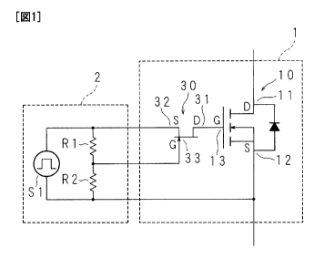
(Embodiment 1) Fig. 1 is a circuit diagram of a semiconductor device
according to Embodiment 1 of the present invention. In the drawing
reference sign 1 designates the semiconductor device, and the
semiconductor device 1 is provided with an N-channel type MOSFET
10 as a switching element which is constituted by a so-called wide
bandgap semiconductor such as silicon carbide, or a semiconductor
material of silicon, and an N-channel type JFET 30 as a semiconductor
element which is constituted by a semiconductor material of silicon
carbide and a drain electrode 31 of which is connected to a gate
13
CA 02764478 2011-12-02
FP 11-0030-00
electrode 13 of MOSFET 10. A drive signal for turning MOSFET 10
on/off is supplied from an external drive circuit 2 to between a source
electrode 32 of JFET 30 and a source electrode 12 of MOSFET 10.
An external load and. anexternal_power supply not shown are connected
to a drain electrode 11 and a source electrode 12 of MOSFET 10.
[0031] The drive circuit 2 is provided with a signal source S1 which
supplies the drive signal to between the source electrode 32 and the
source electrode 12, and a series circuit of resistors R1, R2 which
divides the voltage output from the signal source S l. A connection
point of resistors Rl, R2 and the other end of resistor RI are connected
to a gate electrode 33 and the source electrode 32 of JFET 30,
respectively.
[0032] In the above-described configuration, when the drive signal
output from the signal source Si is an H (high) level, the H level
voltage is divided by the resistors R1, R2 and a divided voltage to the
resistor R1 is applied between the gate electrode 33 and the source
electrode 32. As a consequence, the voltage of gate electrode 33 with
reference to a potential of the source electrode 32 (which will be
referred to hereinafter simply as gate voltage) becomes a negative
voltage. On the other hand, when the drive signal output from the
signal source Si is an L (low) level, a divided voltage to the resistor RI
is approximately zero and thus the gate voltage is approximately zero.
[0033] The below will describe a relation of gate voltage and channel
resistance of JFET 30. Fig. 2 is an explanatory drawing schematically
showing states of change in channel resistance of a typical N-channel
type JFET in accordance with gate voltage. In the drawing the
14
CA 02764478 2011-12-02
FP11-0030-00
horizontal axis represents voltage of the drain electrode with reference
to the potential of the source electrode (which will be referred to
hereinafter simply as drain voltage) Vds (V) and the vertical axis
electric current flowing into the drain electrode (which will be referred-
to hereinafter simply as drain current) Id (A). In Fig. 2, changes of
drain current Id against drain voltage Vds are indicated by solid lines,
using five levels of gate voltage Vgs (0 V, -1 V, -2 V, -3 V, and -4 V)
as parameter. The inverse of gradient of each curve corresponds to the
channel resistance. Since the source electrode and drain electrode of
JFET have approximate symmetry, curves similar to those in Fig. 2 are
also obtained in a case where the horizontal axis represents the voltage
of the source electrode with reference to the potential of the drain
electrode and the vertical axis the electric current flowing into the
source electrode, using voltages of the gate electrode with reference to
the potential of the drain electrode as parameter.
[0034] As shown in Fig. 2, it is seen that when the gate voltage Vgs is
changed with the drain voltage Vds being kept at a constant positive
voltage, the drain current Id varies to a small/large level according to a
low/high level of the gate voltage Vgs, so as to lead to change in
channel resistance to a large/small level. When the gate voltage Vgs is
fixed, the channel resistance is approximately constant and the drain
current Id nearly proportional to the drain voltage Vds flows. It is,
however, noted that in a so-called saturation region, the drain current Id
becomes approximately constant. On the other hand, as the drain
voltage Vds is gradually decreased in the negative voltage range, the
gate electrode and the drain electrode become conducting with the drain
CA 02764478 2011-12-02
FP11-0030-00
voltage Vds becoming smaller than the gate voltage Vgs, to cause the
gate current to flow out from the drain electrode, thus resulting in
sudden increase of negative drain current. This phenomenon tends to
occur in the region where the absolute value -of the. negative gate voltage
Vgs is small. The semiconductor element does not have to be limited
to JFET but may be a depletion type MOSFET. When the
semiconductor element is a depletion type MOSFET, even if the drain
voltage Vds becomes lower than the gate voltage Vgs, the gate electrode
and the drain electrode do not become conducting and there is no
sudden increase of the negative drain current Id with the drain voltage
Vds being negative.
[0035] Referring back to Fig. 1, when the drive signal output from the
signal source Si turns from the L (low) level to the H (high) level so as
to decrease the gate voltage Vgs of JFET 30 to a negative voltage, the
channel resistance of JFET 30 varies from a small value to a large value
with reference to the description of Fig. 2. This allows the MOSFET
10 to be gently turned on with control over the gate current flowing to
the gate electrode 13, whereby a leading edge of a switching waveform
(a decaying edge in the present Embodiment 1) between drain electrode
11 and source electrode 12 comes to have a gentle slope. In this case,
the potential of the source electrode 32 quickly rises to the H level,
while at the drain electrode 31 connected to the gate electrode 13 of
MOSFET 10, a rise of potential lags because of influence of a stray
capacitance of the gate electrode 13, with the result that the drain
voltage Vds of JFET 30 becomes a negative voltage. However, when
the channel resistance of JFET 30 is changed from the small value to the
16
CA 02764478 2011-12-02
FP 11-0030-00
large value, the absolute value of the negative gate voltage Vgs is kept
sufficiently large and therefore an inversion phenomenon in which the
drain voltage Vds of JFET 30 becomes lower than the gate voltage Vgs
is unlikely to occur. Even if such inversion phenomenon occurs, the
potential of the gate electrode 13 will rise because of the electric current
flowing out from the drain electrode 31 of JFET 30, so as to quickly
dissolve the aforementioned inversion phenomenon.
[0036] Next, when the drive signal output from the signal source Si
turns from the H level to the L level, and then the gate voltage Vgs of
JFET 30 rises from the negative voltage to nearly zero, the channel
resistance of JFET 30 varies from the large value to the small value with
reference to the description of Fig. 2. This allows the gate current to
be extracted from the gate electrode 13 by low resistance so as to
quickly turn the MOSFET 10 off, and a trailing edge of the switching
waveform between drain electrode 11 and source electrode 12 (a rising
edge in the present Embodiment 1) comes to have a steep slope. In
this case, the potential of source electrode 32 quickly decays to the L
level, whereas at the drain electrode 31 connected to the gate electrode
13 of MOSFET 10, a decay of potential slightly lags because of
influence of the stray capacitance of gate electrode 13, with the result
that the drain voltage Vds of JFET 30 becomes a positive voltage,
without occurrence of the aforementioned inversion phenomenon.
[0037] The below will describe a mounting example of the
semiconductor device 1 wherein the MOSFET 10 and JFET 30 are
mounted on an identical substrate. Fig. 3 is a schematic plan view of
the semiconductor device 1. The semiconductor device 1 is provided
17
CA 02764478 2011-12-02
FPI1_-0030-00
with a substrate 5 of a ceramic material, and the vertical MOSFET 10
and lateral JFET 30 are individually arranged in proximity on
conductive patterns 51, 52 on the substrate 5. The drain electrode 11
of MOSFET 10. -and the conductive pattern 51, and a substrate of JFET
30 and the conductive pattern 52, are connected each with a
high-temperature solder and/or with an electroconductive adhesive.
The gate electrode 13 and the drain electrode 31 are connected by a lead
61, and the source electrode 12, gate electrode 33, and source electrode
32 are individually connected to respective conductive patterns 53, 54,
and 55 on the substrate 5 by leads 62, 63, and 64, respectively. The
JFET 30 may be a vertical type, and in the case of the vertical type, the
drain electrode 31 directed toward the substrate 5, and the conductive
pattern 52 are connected with a high-temperature solder and the gate
electrode 13 and the conductive pattern 52 are connected by the lead 61.
[0038] In Fig. 3, since the JFET 30 is arranged in proximity to the
MOSFET 10, it is closely subjected to influence of heat generated by
switching of MOSFET 10, but the semiconductor material thereof is
silicon carbide to resist deterioration even at high temperatures of about
400 C, ensuring secure operation as FET.
[0039] In the present Embodiment 1 as described above, the large/small
level of channel resistance is made variable upon propagation of the
MOSFET drive signal through the JFET, so as to allow the change of
the gate current to the small/large level upon on/off control of the
MOSFET, whereby the leading edge of the switching waveform
between the drain electrode and the source electrode of MOSFET comes
to have the gentler slope than the trailing edge thereof. Since the JFET
18
CA 02764478 2011-12-02
FP11-0030-00
is constituted by the wide bandgap semiconductor, the JFET securely
operates without deterioration even if the temperature of JFET increases
as closely subjected to influence of heat generated by the MOSFET
arranged on the same substrate. Therefore, it becomes feasible to
arrange the circuit for preventing false firing, on the same substrate as
the switching element, while avoiding the adverse effect of high
temperatures due to the switching element.
[0040] Since the semiconductor element is the JFET or the depletion
type MOSFET, the channel becomes conducting even if no extra bias
voltage is given as the gate voltage Vgs of FET. Therefore, it becomes
feasible to readily configure the drive circuit of the FET.
[0041] Furthermore, since the JFET as the semiconductor element is
constituted by silicon carbide, it may be securely operated as a variable
resistive element even if the temperature of JFET increases to around
400 C.
[0042] (Modification Example 1)
In Fig. 1, the voltage of the drive signal output from the signal
source Si is divided by the voltage divider consisting of the resistors R1,
R2 and the divided voltage to the resistor RI is used as the gate voltage
Vgs of JFET 30; however, the voltage divider may be omitted in the
case where the voltage of the drive signal is adequately adjusted in
accordance with the change characteristic of channel resistance against
gate voltage Vgs of JFET 30. The below will describe a modification
example without the voltage divider. Fig. 4 is a circuit diagram of the
modification example of the semiconductor device 1 according to
Embodiment 1 of the present invention. The drive signal output from
19
CA 02764478 2011-12-02 -
FP11-0030-00
the signal source Si is supplied to between the source electrode 32 of
JFET 30 and the source electrode 12 of MOSFET 10, which is the same
as in Fig. 1, but the voltage of the drive signal is applied directly
between the gate electrode 33 _and the source electrode 32, which is
different from Fig. 1. Since the circuit of the semiconductor device 1
is the same as in Fig. 1, the description thereof is omitted herein.
[0043] In the above-described configuration, when the drive signal
output from the signal source S1 is the H level, the gate voltage Vgs of
JFET 30 becomes a negative voltage the absolute value of which is
equal to the voltage value of the H level. When the drive signal output
from the signal source Si is the L level, the gate voltage Vgs becomes
approximately zero, which is the same as in Fig. 1. In this case, the
crest value of the H level of the drive signal is adjusted in such a
manner that the channel resistance of JFET 30 becomes a desired large
value by the negative gate voltage Vgs with the drive signal from the
signal source S1 turning to the H level. Conversely, the change
characteristic of channel resistance against gate voltage Vgs of JFET 30
may be adjusted in accordance. with the crest value of the H- level of the
drive signal. This adjustment allows omission of the resistors R1, R2
in the drive circuit 2.
[0044] (Embodiment 2)
Embodiment 1 is the mode wherein the channel types
(N-channel type/P-channel type) of MOSFET 10 and JFET 30 both are
the N-channel types, whereas Embodiment 2 is a mode wherein the
channel types of MOSFET and JFET are made different from each other,
and a mode wherein the both are the P-channel types.
CA 02764478 2011-12-02
FP11-0030-00
[0045] Fig. 5 is a table to illustrate gate voltages of JFETs, with on/off
states of MOSFETs by the drive signal propagating in the channel of
JFETs. The same also applies to the case where the JFET is the
depletion type MOSFET In the table each row, and each column
represent the channel types of JFET and MOSFET, respectively. Fig. 5
shows the gate voltages applied when the MOSFET is turned on/off or
off/on by the drive signal of the H/L level. Fig. 5 shows the example
of gate voltages of JFETs with supply of the MOSFET drive signal to
the source electrode of JFETs, and, since the source electrode and drain
electrode of JFETs have approximate symmetry, a table similar to that in
Fig. 5 is also obtained in an example to illustrate gate voltages (to the
potential of the drain electrode) with supply of the MOSFET drive
signal to the drain electrode.
[0046] For example, in the circuit diagrams of Figs. 1 and 4 in
Embodiment 1, when the N-channel type MOSFET 10 is turned on/off
by the drive signal propagating in the channel of the N-channel type
JFET 30, the gate voltage Vgs becomes the negative voltage with the
drive signal at the H level and the gate voltage Vgs becomes the zero
voltage with the drive signal at the L level. Namely, the channel
resistance of JFET 30 is changed to the large/small value by changing
the gate voltage Vgs to the low/high level, with respect to the drive
signal of the H/L level for on/off control of the MOSFET 10. The
below will describe a configuration of a combination of a P-channel
type JFET and an N-channel type MOSFET, and a configuration of a
combination of a P-channel type JFET and a P-channel type MOSFET.
A circuit diagram of the configuration of the combination of N-channel
21
CA 02764478 2011-12-02
FP1I-0030-00
type JFET and P-channel type MOSFET may be readily contemplated
from circuit diagrams of configurations of other combinations, and
therefore specific illustration thereof is omitted herein.
[0047] First described is the case of the combination of P-channel type
JFET and N-channel type MOSFET. Fig. 6 is a circuit diagram of the
semiconductor device according to Embodiment 2 of the present
invention. In the drawing reference sign 1 a designates the
semiconductor device, and the semiconductor device 1 a is provided
with the N-channel type MOSFET 10, and a P-channel type JFET 40
which is constituted by the semiconductor material of silicon carbide
and a drain electrode 41 of which is connected to the gate electrode 13
of MOSFET 10. A drive signal to turn the MOSFET 10 on/off is
supplied from an external drive circuit 2a to between a source electrode
42 of JFET 40 and the source electrode 12 of MOSFET 10. An
external load and an external power supply not shown are connected to
the drain electrode 11 and the source electrode 12 of MOSFET 10.
[0048] The drive circuit 2a is provided with the signal source S1 to
supply the drive signal to between the source electrode 42 and the
source electrode 12, and a series circuit of resistors R3, R4 to divide a
difference between voltage from an unrepresented positive power
supply and the voltage output from the signal source St. A connection
point of the resistors R3, R4 and the other end of the resistor R3 are
connected to a gate electrode 43 and the source electrode 42 of JFET 40,
respectively. The voltage of the positive power supply is set higher
than the voltage of the H level of the drive signal. The drive circuit 2a
is further provided with an NPN type transistor Q1 whose base and
22
CA 02764478 2011-12-02
FP11-0030-00
emitter are connected through a resistor R5 as a base resistor to the
signal source S 1, and an NPN type transistor Q2 whose base and emitter
are connected to a collector and the emitter of the transistor Ql,
respectively. The collector of transistor Q1 is connected through a
resistor R6 to the positive power supply, and the collector of transistor
Q2 is connected to the gate electrode 43.
[0049] In the above-described configuration, an inverted signal
resulting from inversion of the HIL level of the drive signal output from
the signal source Sl is output at the collector of transistor Q1, and a
signal of the H/L level resulting from inversion of the L/H level of the
inverted signal is output at the collector of transistor Q2. Namely,
when the drive signal output from the signal source S 1 is the H level,
the signal output from the collector of transistor Q2 is the H level (open
collector). In this case, the difference between the voltage of the
positive power supply and the voltage of the H level is divided by the
resistors R3, R4 and the divided voltage to the resistor R3 is applied
between the gate electrode 43 and the source electrode 42, whereby the
gate voltage Vgs becomes a positive voltage. On the other hand, when
the drive signal output from the signal source S 1 is the L level, the
collector of transistor Q2 becomes the L level and thus the source
electrode 42 and the gate electrode 43 both are the L level, with the
result that the gate voltage Vgs of JFET 40 is approximately zero.
[0050] In other words, when the N-channel type MOSFET 10 is turned
on/off by the drive signal propagating in the channel of the P-channel
type JFET 40, the gate voltage Vgs of JFET 40 becomes the positive
voltage with the drive signal at the H level, and the gate voltage Vgs
23
CA 02764478 2011-12-02
FP 1 i-0030-00
becomes the zero voltage with the drive signal at the L level. Namely,
as shown in Fig. 5, the channel resistance of JFET 40 may be changed
to the large/small value by changing the gate voltage Vgs to the
high/low level, with respect to the drive signal of the H/L level for-
on/off control of MOSFET 10.
[0051] The following will describe the case of the combination of
P-channel type JFET and P-channel type MOSFET. Fig. 7 is a circuit
diagram of another semiconductor device according to Embodiment 2
of the present invention. In the drawing reference sign lb designates
the semiconductor device, and the semiconductor device lb is provided
with a P-channel type MOSFET 20, and the P-channel type JFET 40
which is constituted by the semiconductor material of silicon carbide
and the drain electrode 41 of which is connected to a gate electrode 23
of MOSFET 20. A drive signal to turn the MOSFET 20 on/off is
supplied from an external drive circuit 2b to between the source
electrode 42 of JFET 40 and a source electrode 22 of MOSFET 20.
An external load and an external power supply not shown are connected
to a drain electrode 21 and the source electrode 22 of MOSFET 20.
[0052] The drive circuit 2b is provided with a signal source S2 to
supply the drive signal to between source electrode 42 and the source
electrode 22, and a series circuit of resistors R7, R8 to divide the voltage
output from the signal source S2. A connection point of the resistors
R7, R8 and the other end of the resistor R7 are connected to the gate
electrode 43 and the source electrode 42 of JFET 40, respectively.
[0053] In the above-described configuration, when the drive signal
output from the signal source S2 is the L level, the voltage of the L level
24
CA 02764478 2011-12-02
FP11-0030-00
is divided by the resistors R7, R8 and the divided voltage to the resistor
R7 is applied between the gate electrode 43 and the source electrode 42,
whereby the gate voltage Vgs becomes a positive voltage. On the
other hand, when the drive signal output from the signal source S2 is the
H level, since the divided voltage to the resistor R7 is approximately
zero, the gate voltage Vgs is approximately zero.
[0054] In other words, when the P-channel type MOSFET 20 is turned
on/off by the drive signal propagating in the channel of the P-channel
type JFET 40, the gate voltage Vgs of JFET 40 becomes the positive
voltage with the drive signal at the L level, and the gate voltage Vgs
becomes the zero voltage with the drive signal at the H level. Namely,
as shown in Fig. 5, the channel resistance of JFET 40 may be changed
to the large/small value by changing the gate voltage Vgs to the
high/low level, with respect to the drive signal of the L/H level for
on/off control of MOSFET 20.
[0055] The other portions corresponding to those in Embodiment 1 are
denoted by the same reference signs, and the detailed description
thereof is omitted herein.
[0056] In the present Embodiment 2 as described above, since the drain
and source of N-channel (or P-channel) type JFET have approximate
symmetry, the FET channel resistance upon on/off control of MOSFET
may be changed to the large/small value when the gate voltage with
reference to the potential of the source electrode or drain electrode of
JFET provided with the drive signal for on/off control of MOSFET is
changed to the low/high (or high/low) level.
[0057] (Embodiment 3)
CA 02764478 2011-12-02
FP 11-0030-00
Embodiment 1 is the mode using the JFET 30 as semiconductor
element, whereas Embodiment 3 is a mode using Schottky barrier
diodes connected in antiparallel connection as semiconductor elements.
Fig. 8 is a circuit diagram of a semiconductor device according to
Embodiment 3 of the present invention. In the drawing reference sign
1c designates the semiconductor device, and the semiconductor device
1c is provided with the N-channel type MOSFET 10, and Schottky
barrier diodes D1, D2 constituted by the semiconductor material of
silicon carbide and connected in antiparallel connection. The Schottky
barrier diodes D1, D2 have a cathode and an anode, respectively,
connected to the gate electrode 13 of MOSFET 10. A drive signal to
turn the MOSFET 10 on/off is supplied from the external signal source
Si to between an anode and a cathode of the respective Schottky barrier
diodes D1, D2, and the source electrode 12 of MOSFET 10. An
external load and an external power supply not shown are connected to
the drain electrode 11 and the source electrode 12 of MOSFET 10.
[0058] In the above-described configuration, when the drive signal
output from the signal source S1 turns from the L level to the H level,
the Schottky barrier diode D1 with a relatively large on-resistance
becomes conducting, whereby the gate current flowing to the gate
electrode 13 is controlled to gently turn the MOSFET 10 on. When the
drive signal output from the signal source Si turns from the H level to
the L level, the Schottky barrier diode D2 with a relatively small
on-resistance becomes conducting, whereby the gate current is extracted
from the gate electrode 13 by low resistance to quickly turn the
MOSFET 10 off. In the case where the MOSFET 10 is the P-channel
26
CA 02764478 2011-12-02
FP11-0030-00
type, the same effect as above is achieved by setting the on-resistance of
the Schottky barrier diode D1 relatively small and the on-resistance of
the Schottky barrier diode D2 relatively large.
[0059] The following will describe the on-resistances of Schottky
barrier diodes D1, D2. Fig. 9 is a vertical cross-sectional view
schematically showing the configuration of Schottky barrier diodes Dl,
D2. In the drawing reference numeral 71 designates an n+ type
semiconductor layer, and an n- type semiconductor layer 72 is laid on a
top surface of the n+ type semiconductor layer 71. A bottom surface
of the n+ type semiconductor layer 71 is covered by a back metal
electrode layer 70 serving as a cathode, and a metal electrode film 73
serving as an anode is formed in a central region on the top surface of
the n- type semiconductor layer 72. The other region on the top
surface of the n- type semiconductor layer 72 is covered by insulating
film 74 constituted by silicon oxide.
[0060] The n+ type semiconductor layer 71 and the n- type
semiconductor layer 72 have their respective equivalent resistances
represented by n+ layer resistance 81 and n- layer resistance 82, for an
on-state current to flow from the metal electrode film 73 to the back
metal electrode layer 70. The back metal electrode layer 70 and the
metal electrode film 73 have their respective equivalent resistances
represented by back metal electrode layer resistance 80 and metal
electrode film resistance 83. These equivalent resistances are
considered to be on-resistances connected in series, for the on-state
current. The on-resistances of Schottky barrier diodes Dl, D2 may be
resistances that may be varied by adjusting the resistivity and/or the
27
CA 02764478 2011-12-02
FP11-0030-00
thickness of the n- type semiconductor layer (referred to hereinafter as
n- layer) 72 at the time of manufacture.
[0061] Fig. 10 is an explanatory diagram schematically showing states
of change in the on-resistances of Schottky barrier diodes DI, D2
according to the resistivity and/or the thickness of n- layer 72. In the
drawing the horizontal axis represents forward voltage VF (V) and the
vertical axis forward current IF (A). In Fig. 10, a solid line indicates a
case of resistivity and/or thickness of n- layer 72 being relatively small,
and a dashed line a case of resistivity and/or thickness of n- layer 72
being relatively large. The inverses of gradients of the solid line and
the dashed line correspond to on-resistances. Namely, it is seen that
the gradient of forward current IF against forward voltage VF varies
from a large value to a small value so as to change the on-resistance
from a small value to a large value, according to change in resistivity
and/or thickness of n- layer 72 from a small level to a large level.
[0062] The below will describe a mounting example of the
semiconductor device lc in which the MOSFET 10 and Schottky barrier
diodes Dl, D2 are mounted on an identical substrate. Fig. 11 is a
schematic plan view of the semiconductor device lc. The
semiconductor device lc is provided with a substrate 5a constituted by a
ceramic material, and the vertical MOSFET 10 and Schottky barrier
diodes Dl, D2 are individually arranged in proximity on respective
conductive patterns 51, 56, and 57 on the substrate 5a. The drain
electrode 11 of MOSFET 10 and the conductive pattern 51, and the back
metal electrode layers 70, 70 of Schottky barrier diodes Dl, D2 and the
conductive patterns 56, 57 are connected each with a high-temperature
28
CA 02764478 2011-12-02
FP11-0030-00
solder.
[0063] The source electrode 12 and the gate electrode 13 are connected
to respective conductive patterns 53, 58 on the substrate 5a by leads 62,
65, respectively. The conductive patterns 56, 58 are connected by a
lead 66, and the conductive pattern 58 and the metal electrode film 73 of
Schottky barrier diode D2 are connected by a lead 67. The metal
electrode film 73 of Schottky barrier diode Dl and conductive pattern
59 on the substrate 5a are connected by a lead 68, and the conductive
patterns 57, 59 are connected by a lead 69.
[0064] Since the Schottky barrier diodes Dl, D2 are arranged in
proximity to the MOSFET 10, they are closely subjected to influence of
heat generated by switching of MOSFET 10, but, because the Schottky
barrier diodes Dl, D2 are constituted by the semiconductor material of
silicon carbide, they securely operate as diodes with different
on-resistances, without risk of deterioration even at high temperatures of
about 400 C.
[0065] The other portions corresponding to those in Embodiment 1 are
denoted. by the. same reference. signs, and the detailed description
thereof is omitted herein.
[0066] According to the present Embodiment 3 as described above,
since the MOSFET is of the N-channel (or P-channel) type, the gate
current upon on/off control of MOSFET flows in the forward/backward
direction (or in the backward/forward direction) to the MOSFET.
Furthermore, the Schottky barrier diodes are connected in antiparallel
connection and the forward resistance becomes larger (or smaller) than
the backward resistance to the MOSFET. Therefore, the gate current
29
CA 02764478 2011-12-02
FP11-0030-00
upon on/off control of MOSFET may be changed to a small/large level
by the resistances of the Schottky barrier diodes.
[0067] Embodiments 1 to 3 employed the MOSFET 10 or 20 as a
switching element, but, the switching element does not have to be
limited to this; it is also possible to employ a bipolar device with an
insulated gate such as IGBT.
[0068] The above-described Embodiments 1, 2 will be described below
using another expression. The semiconductor device 1 in Embodiment
1 will be described as an example, but the same also applies to the
semiconductor devices la, lb in Embodiment 2. As shown in Fig. 1,
the semiconductor device 1 is provided with the MOSFET 10 and a
semiconductor circuit. The MOSFET 10 is an insulated gate type
semiconductor element provided on the substrate 5. The
semiconductor circuit includes the JFET 30 as one semiconductor
element. The JFET 30 contains a semiconductor material with a larger
bandgap than silicon and is provided on the substrate 5. As shown in
Fig. 5, this semiconductor circuit receives the drive signal having the H
level (the high level) and the L level (the low level) at an input of this
semiconductor circuit, and generates a signal to control the
conduction/non-conduction state of the switching element at an output
of this semiconductor circuit. As shown in Fig. 5, conduction
represents the on state of MOSFET 10 and non-conduction the off state
of MOSFET 10. The drive signal includes a first transition from one
to the other between the H level and the L level, and a second inverse
transition between the H level and the L level. For example, when the
first transition is a transition from the H level to the L level, the second
CA 02764478 2011-12-02
FP11-0030-00
transition is a transition from the L level to the H level. The drive
signal propagates from the input of the semiconductor circuit to the
output of the semiconductor circuit, through the JFET 30. In the
semiconductor circuit, as shown in Fig. 5, the JFET 30 changes from a
first to a second of two conduction states in response to the first
transition of the drive signal in propagation of the drive signal in JFET
30, and the JFET 30 changes from the second to the first of the two
conduction states in response to the second transition of the drive signal
in propagation of the drive signal in JFET 30, so that the semiconductor
circuit has variable resistance of the semiconductor circuit to the
propagation of the drive signal, whereby a signal to control
conduction/non-conduction of the switching element according to this
resistance change results at the output of the semiconductor circuit.
The two conduction states of the semiconductor circuit are generated
according to the resistance of the semiconductor circuit to the
propagation of the drive signal. As shown in Fig. 5, when the
MOSFET 10 turns to the on state, the resistance of the semiconductor
circuit to the propagation of the drive signal is relatively large; when the
switching element turns to the off state, the resistance of the
semiconductor circuit to the propagation of the drive signal is relatively
small.
[0069] The semiconductor circuit includes the N-channel type JFET 30,
as shown in Fig. 1, but it may have the configuration including the
P-channel type JFET 40, instead of the JFET 30, as shown in Figs. 6 and
7. The semiconductor material of JFETs 30, 40 is silicon carbide.
The semiconductor circuit includes the N-channel type MOSFET 10 as
31
CA 02764478 2011-12-02
FP11-0030-00
a switching element, as shown in Fig. 1, but it may have the
configuration using the P-channel type MOSFET 20, instead of the
MOSFET 10, as shown in Fig. 7.
[0070] The JFET 30, as shown in Fig. 1, has the gate electrode 33, drain
electrode 31, and source electrode 32. The semiconductor circuit has
another input to receive the gate signal (signal generated from the drive
signal) for the gate electrode 33 of JFET 30. In the JFET 30, as shown
in Fig. 2, the resistance of the channel of JFET 30 varies according to
the level of the gate signal (one of Vgd and Vgs) with reference to the
potential of either one of the drain electrode 31 and the source electrode
32. On the other hand, as shown in Figs. 6 and 7, when the
semiconductor element is of the P-channel type, this semiconductor
element is JFET 40. The JFET 40 has the gate electrode 43, drain
electrode 41, and source electrode 42. The semiconductor circuit has
another input to receive the gate signal (signal generated from the drive
signal) for the gate electrode 43 of JFET 40. In the JFET 40, the
resistance of the channel of JFET 40 varies according to the level of the
gate. signal (one of Vgd and Vgs) with reference to the potential of
either one of the drain electrode 41 and the source electrode 42. In the
case of the N-channel type JFET 30, as shown in Fig. 1, the drive signal
propagates from one of the source electrode 32 and drain electrode 31 of
JFET 30 to the other of the source electrode 32 and drain electrode 31 of
JFET 30 and is subjected to voltage division, to be fed as a gate signal
to the gate electrode 33. On the other hand, in the case of the
P-channel type JFET 40, as shown in Figs. 6 and 7, the drive signal
propagates from one of the source electrode 42 and drain electrode 41 of
32
CA 02764478 2011-12-02
FP11-0030-00
JFET 40 to the other of the source electrode 42 and drain electrode 41 of
JFET 40 and is subjected to voltage division, to be fed as a gate signal
to the gate electrode 43. A depletion type MOSFET may be used
instead of the insulated gate type JFET 30 and JFET 40. In this case,
the drive signal propagates from one of the source electrode and drain
electrode of the depletion type MOSFET to the other of the source
electrode and the drain electrode of the depletion type MOSFET and is
subjected to voltage division, to be fed as a gate signal to the gate
electrode of the depletion type MOSFET.
[0071 ] Next, the action and effect will be further described, for example,
in the case of Embodiment 1. When the drive signal output from the
signal source S1 turns from the L level to the H level to decrease the
gate voltage Vgs of JFET 30 to the negative voltage, the channel
resistance of JFET 30 increases with reference to the description of Fig.
2. This allows the MOSFET 10 to be gently turned on by controlling
the gate current flowing to the gate electrode 13 of MOSFET 10,
whereby the leading edge of the switching waveform between the drain
electrode 11 and source electrode 12 of MOSFET 10 comes to have a
gentle slope. When the drive signal output from the signal source S 1
turns from the H level to the L level, and thus the gate voltage Vgs of
JFET 30 rises from the negative voltage to nearly zero, the channel
resistance of JFET 30 decreases with reference to the description of Fig.
2. This allows the MOSFET 10 to be quickly turned off by extracting
the gate current from the gate electrode 13 of MOSFET 10 by low
resistance, whereby the trailing edge of the switching waveform
between the drain electrode 11 and the source electrode 12 of MOSFET
33
CA 02764478 2011-12-02
FPII-0030-00
comes to have a steep slope.
[0072] The configurations of Embodiments 1, 2 will be described using
still another expression. For example, the semiconductor device 1 in
Embodiment 1 shown in Fig. 1 will be described below, but the same
5 also applies to the semiconductor devices la, lb in Embodiment 2
shown in Figs. 6 and 7. As shown in Fig. 1, the semiconductor device
1 is provided with the MOSFET 10 and a semiconductor circuit. The
MOSFET 10 is an insulated gate type semiconductor element provided
on the substrate 5. The semiconductor circuit has the JFET 30. The
10 JFET 30 contains a semiconductor material with a larger bandgap than
silicon, and is provided on the substrate 5. The JFET 30 has the source
electrode 32, drain electrode 31, and gate electrode 33. One of the
source electrode 32 and the drain electrode 31 of JFET 30 receives the
drive signal having the H level (the high level) and the L level (the low
level). The drive signal propagates from the input of the
semiconductor circuit to the output of the semiconductor circuit through
the JFET 30. The other of the source electrode 32 and the drain
electrode 31 of JFET 30 provides a signal to control
conduction/non-conduction of JFET 30 according to the drive signal.
The JFET 30 shown in Fig. 1 is of the N-channel type, but it may have
the configuration using the P-channel type JFET 40 in Embodiment 2
shown in Figs. 6 and 7, instead of the JFET 30. It is also possible to
adopt the configuration using the P-channel type MOSFET 20 in
Embodiment 2 shown in Fig. 7, instead of the N-channel type MOSFET
10.
[0073] Next, Embodiment 3 described above will be explained using
34
CA 02764478 2011-12-02
FP11-0030-00
another expression. As shown in Fig. 8, the semiconductor device I c
is provided with the MOSFET 10 and a semiconductor circuit. The
MOSFET 10 is an insulated gate type switching element provided on
the substrate 5a. The semiconductor circuit has the Schottky barrier
diodes D1, D2. The Schottky barrier diodes Dl, D2 contain a
semiconductor material with a larger bandgap than silicon, and are
provided on the substrate 5a. The semiconductor circuit receives the
drive signal having the H level (the high level) and the L level (the low
level) at an input of the semiconductor circuit, and generates a signal to
control conduction/non-conduction of MOSFET 10 at an output of the
semiconductor circuit. Conduction represents the on state of MOSFET
10 and non-conduction the off state of MOSFET 10. The drive signal
includes a first transition from one to the other between the H level and
the L level, and a second inverse transition between the H level and the
L level. For example, when the first transition is a transition from the
H level to the L level, the second transition is a transition from the L
level to the H level. The drive signal propagates from the input of the
semiconductor . circuit to the output of the semiconductor circuit,
through either one of the Schottky barrier diodes Dl, D2 in the
semiconductor circuit. In the semiconductor circuit, the circuit
changes from a first to a second of two conduction states in response to
the first transition of the drive signal in propagation of the drive signal
in each of the Schottky barrier diodes Dl, D2, and the circuit changes
from the second to the first of the two conduction states in response to
the second transition of the drive signal in propagation of the drive
signal in each of the two semiconductor elements, so that the
CA 02764478 2011-12-02
FP 11-0030-(100
semiconductor circuit has variable resistance of the semiconductor
circuit to the propagation of the drive signal, whereby the signal to
control conduction/non-conduction of MOSFET 10 results at the output
of the semiconductor circuit according to the resistance change. The
semiconductor circuit is composed of the parallel circuit in which the
Schottky barrier diodes Dl, D2 are connected in parallel. The
Schottky barrier diodes D1, D2 are connected in directions opposite to
each other and in parallel with each other. The drive signal propagates
from the input of the parallel circuit to the output of the parallel circuit.
The two conduction states of the semiconductor circuit are generated
according to the resistance of the semiconductor circuit to the
propagation of the drive signal. The resistance of the semiconductor
circuit to the propagation of the drive signal is generated according to
the direction of the drive signal flowing in the Schottky barrier diodes
Dl, D2 constituting the semiconductor circuit. Namely, the
conduction state of the semiconductor circuit varies from the first to the
second of the two conduction states, or from the second to the first of
the two conduction states, according to change in the direction of the
drive signal propagating in the semiconductor circuit.
[0074] The MOSFET 10 is an N-channel type switching element,
whereas, in the case where a P-channel type switching element is used,
the MOSFET 20 is used instead of the MOSFET 10. The
semiconductor material of Schottky barrier diodes Dl, D2 is silicon
carbide. When the N-channel type MOSFET 10 is used as the
switching element, the Schottky barrier diode D1 is connected in the
forward direction to the MOSFET 10, the Schottky barrier diode D2 is
36
CA 02764478 2011-12-02
FPII-0030-00
connected in the backward direction to the MOSFET 10, and the
resistance of the Schottky barrier diode Dl is larger than that of the
Schottky barrier diode D2. When the P-channel type MOSFET 20 is
used, the Schottky barrier diode D2 is connected in the forward
direction to the MOSFET 20, the Schottky barrier diode DI is
connected in the backward direction to the MOSFET 20, and the
resistance of the Schottky barrier diode D2 is larger than that of the
Schottky barrier diode Dl.
[0075] Next, the action and effect of Embodiment 3 will be further
described. For example, in the case where the N-channel type
MOSFET 10 is used as the switching element, when the drive signal
output from the signal source Si turns from the L level to the H level,
the Schottky barrier diode D1 with the relatively large on-resistance
becomes conducting (in this case, the Schottky barrier diode D2 is
non-conducting), whereby the MOSFET 10 is gently turned on by
controlling the gate current flowing to the gate electrode 13. When the
drive signal output from the signal source S I turns from the H level to
the L level, the Schottky barrier diode D2 with the relatively small
on-resistance becomes conducting (in this case, the Schottky barrier
diode D1 is non-conducting), whereby the MOSFET 10 is quickly
turned off by extracting the gate current from the gate electrode 13 by
low resistance. In the case where the P-channel type MOSFET 20 is
used as the switching element, the same effect is achieved as in the case
using the MOSFET 10, by setting the on-resistance of the Schottky
barrier diode Dl relatively small and the on-resistance of the Schottky
barrier diode D2 relatively large.
37
CA 02764478 2011-12-02
FP11-0030-00
[0076] Embodiment 3 will be described using still another expression.
As shown in Fig. 8, the semiconductor device 1 c is provided with the
N-channel type MOSFET 10 as an insulated gate type switching
element provided on the substrate 5a (the MOSFET 20 in the case of the.
P-channel type), and a semiconductor circuit having the Schottky barrier
diodes Dl, D2 containing the semiconductor material with the larger
bandgap than silicon and provided on the substrate 5a. The Schottky
barrier diodes Dl, D2 constitute a parallel circuit in which they are
connected in directions opposite to each other and in parallel with each
other. Namely, the semiconductor circuit consists of this parallel
circuit. In the case where one of the Schottky barrier diodes DI, D2 is
connected in the forward direction to the MOSFET 10 and the other of
the Schottky barrier diodes Dl, D2 is connected in the backward
direction to the switching element, the resistance of the forward
Schottky barrier diode is larger than that of the backward Schottky
barrier diode. The semiconductor circuit receives the drive signal
having the H level (the high level) and the L level (the low level), at its
input. The drive signal propagates from the input of the semiconductor
circuit to the output of the semiconductor circuit through the parallel
circuit. The output of the semiconductor circuit controls
conduction/non-conduction of the switching element, according to the
drive signal.
Industrial Applicability
[0077] The semiconductor device is one avoiding the adverse effect of
high temperatures due to the switching element and having the circuit to
prevent the false firing, arranged on the same substrate as the switching
38
CA 02764478 2011-12-02
FPli-0030-00
element.
List of Reference Signs
[0078] 1, la, 1b, lc semiconductor device.
5, 5a substrate.
10, 20 MOSFET (switching element).
13, 23 gate electrode (insulated gate).
30, 40 JFET (semiconductor element).
31, 41 drain electrode.
32, 42 source electrode.
33, 43 gate electrode.
D15 D2 Schottky barrier diodes.
39