Note: Descriptions are shown in the official language in which they were submitted.
CA 02764504 2015-12-04
DC VOLTAGE SOURCE CONVERTER
The invention relates to a direct current
(DC) voltage source converter for use in high voltage
direct current (HVDC) power transmission.
In power transmission networks, AC power is
typically converted to direct current (DC) power for
transmission via overhead lines and/or under-sea
cables. This conversion means that it is not necessary
to compensate for AC capacitive load effects that are
otherwise imposed by the transmission line or cable.
This in turn reduces the cost per kilometer of the
lines and/or cables and thus conversion of AC power to
DC power becomes cost-effective when power needs to be
transmitted over a long distance.
DC transmission and distribution networks
are needed to support the emergence of HVDC power
transmission. These DC transmission and distribution
networks however often operate at different voltage
levels, which can create difficulties when
interconnecting the DC networks to form a DC power
grid.
It is therefore desirable to provide a DC
voltage source converter for use in HVDC power
transmission that is operable to facilitate the
transfer of electrical power between DC networks
operating at different voltage levels.
One solution lies in the use of a
transformer within a DC to DC power converter.
Transformers operate to step up or step
down AC voltages and thereby facilitate the
CA 02764504 2011-12-05
WO 2010/145690
PCT/EP2009/057388
2
interconnection of AC networks operating at different
voltage levels. In order to interconnect DC networks
operating at different voltage levels using a
transformer, the DC power must be converted to AC power
on each side of the transformer so as to enable the
transformer to effect the necessary step up or step
down in AC voltage between the two networks.
The inclusion of AC to DC voltage
converters, in addition to a transformer, increases the
size, weight and cost of the DC power transmission
infrastructure, and therefore results in an undesirable
arrangement.
Another solution lies in the use of a
direct DC to DC power converter arrangement 20, such as
that shown in Figure 1, which includes an inductor 22
connected in series, and a capacitor 24 connected in
parallel, between two DC terminals 26,28. Arrangements
of this type are often used in applications such as
traction drives to step up or step down the DC voltage
in order to optimize the operation of the DC network
and connected electrical loads.
The arrangement shown in Figure 1 avoids
the need for intermediate DC to AC converters and
therefore results in a smaller, lighter and less costly
arrangement than would otherwise be obtained through
the use of a transformer.
Conventional DC to DC power converters,
such as the DC to DC power converter shown in Figure 1,
are however designed for operation at 10's or 100's of
kW. In contrast, HVDC power transmission typically
involves 10's or 100's of MW.
CA 02764504 2011-12-05
WO 2010/145690
PCT/EP2009/057388
3
It is possible to modify the direct DC to
DC power converter shown in Figure 1 to operate at
higher levels of power. This may be done by replacing
electronic switches 21, 23 connected in parallel and
series branches between the DC terminals with high
power electronic switches provided in the form of
multiple insulated-gate bipolar transistors (IGBTs)
connected in series. The connection of IGBT devices in
series strings however often requires complex active
gate drives and large passive components to control
voltage sharing between the multiple transistors, and
again therefore results in an undesirable arrangement.
According to an aspect of the invention,
there is provided a DC voltage source converter for use
in high voltage DC power transmission comprising at
least one chain-link converter connected between first
and second DC terminals, the or each chain-link
converter including a chain of modules connected in
series and each module including at least one pair of
semiconductor switches connected in parallel with an
energy storage device, wherein the or each chain-link
converter is operable when DC networks are connected to
the first and second DC terminals to control switching
of the modules to selectively charge or discharge the
energy storage device of one or more of the modules, as
required, to offset any difference in the DC voltage
levels of the DC networks.
The use of a chain-link converter including
a plurality of individual modules allows different
levels of voltage to be constructed. High voltage
levels in power transmission can therefore be
CA 02764504 2011-12-05
WO 2010/145690
PCT/EP2009/057388
4
accommodated by increasing the number of modules in the
chain-link converter.
The chain-link converter can be made to
operate as a voltage multiplier circuit simply by
allowing the energy storage device in each module of
the chain to independently charge to the supply voltage
rail by putting the adjacent modules into a bypass
state. An output supply voltage may then by constructed
by connecting the energy storage devices of a number of
individual modules in series to produce a controlled
output voltage. Given that the individual energy
storage devices will inherently discharge during this
period, the number of modules connected in series can
be progressively increased to maintain the desired
output voltage profile if desired.
Switching strategies that equalize the
charge transfer during both the charging and
discharging cycles are necessary to ensure voltage
equalization.
The semiconductor switches are preferably
constructed from insulated-gate bipolar transistors.
However, in other embodiments, the switches may be
constructed from gate turn-off thyristors or field-
effect transistors.
The or each pair of semiconductor switches
in each module is controllable to insert an energy
storage device into the circuit or to cause a short
circuit to bypass the energy storage device.
The energy storage device provided in each
module is preferably a capacitor, but in other
embodiments may be a fuel cell, a battery or an AC
CA 02764504 2011-12-05
WO 2010/145690
PCT/EP2009/057388
electrical generator and rectifier, each device being
additionally capable of providing a source of real
power.
The use of a chain-link type converter
5 allows the use of a converter that is unidirectional
(i.e. produces voltage steps in one polarity only) or
bidirectional (i.e. produces voltage steps in both
positive and negative polarities).
In order to provide a unidirectional
single-phase multilievel converter, the semiconductor
switches of each module may preferably be connected
with the respective energy storage device in a half-
bridge arrangement to define a 2-quadrant unipolar
module that can develop zero or positive voltage but
can conduct current in both directions.
In order to provide a bidirectional single-
phase multilevel converter, the semiconductor switches
of each module may preferably be connected with the
respective energy storage device in a full-bridge
arrangement to define a 4-quadrant bipolar module that
can develop positive or negative voltage and can also
conduct current in both directions.
The bidirectional characteristic of the 4-
quadrant bipolar module is advantageous because it may
be utilized to provide voltage inversion and to provide
a voltage step up and step down capability in the same
DC voltage source converter.
Preferably the DC voltage source converter
includes a switching assembly to toggle between
electrical charging and discharging of the or each
module.
CA 02764504 2011-12-05
WO 2010/145690
PCT/EP2009/057388
6
The switching assembly allows the timing of
the charging and discharging operations to be
manipulated in a controlled manner, and in embodiments
of the invention may include one or more diodes.
The use of one or more diodes provides an
automatic switching system whereby the operation of the
DC voltage source converter switches between module
charging and discharging by forward or reverse biasing
the diode, which alters the direction of current flow.
In embodiments of the invention a chain-
link converter may be connected in parallel with the
first DC terminal and may be connected in parallel with
a series arrangement of the second DC terminal and the
switching assembly.
This arrangement creates a parallel
converter which allows electrical power to be
transferred from a lower DC voltage to a higher DC
voltage.
In other embodiments of the invention a
series arrangement of a chain-link converter and the
second DC terminal may be connected in parallel with
the first DC terminal and may be connected in parallel
with the switching assembly.
This arrangement creates a parallel
converter which allows electrical power to be
transferred from a higher DC voltage to a lower DC
voltage.
In further embodiments of the invention a
first chain-link converter may be connected in parallel
with the first DC terminal and may be connected in
CA 02764504 2011-12-05
WO 2010/145690
PCT/EP2009/057388
7
parallel with a series arrangement of the second DC
terminal and a second chain-link converter.
This arrangement combines the functions of
the parallel and series converters, resulting in a
flexible DC voltage source converter.
In yet further embodiments the DC voltage
source converter may include one or more inductors
connected in series with either or each of the first
and second DC terminals. The inclusion of an inductor
helps to regulate the flow of current flowing into the
DC networks.
Preferred embodiments of the invention will
now be described, by way of non-limiting examples, with
reference to the accompanying drawings in which:
Figure 1 shows, in schematic form, a prior
art voltage source converter for DC to DC voltage
conversion in the 10's to 100's of kW range;
Figure 2A shows the structure of a 2-
quadrant unipolar module and its location in a chain-
link converter;
Figure 2B shows the structure of a 4-
quadrant bipolar module and its location in a chain-
link converter;
Figure 3 shows a parallel DC voltage source
converter according to a first embodiment of the
invention;
Figure 4A and 4B shows the charging and
discharging steps of a parallel DC voltage source
converter;
CA 02764504 2011-12-05
WO 2010/145690
PCT/EP2009/057388
8
Figure 5A and 5B shows the bidirectional
discharge capability of a parallel DC voltage source
converter based on full-bridge elements;
Figure 6 shows a series DC voltage source
converter according to a second embodiment of the
invention;
Figure 7 shows the charging and discharging
steps of a series DC voltage source converter; and
Figure 8 shows a DC voltage source
converter according to a third embodiment of the
invention.
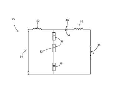
A DC voltage source converter 30 for use in
high voltage DC power transmission according to an
embodiment of the invention is shown in Figure 3. The
converter 30 includes a chain-link converter 32
connected between first and second DC terminals 34, 36.
The chain-link converter 32 includes a chain of modules
38 connected in series, each module 38 including at
least one pair of semiconductor switches 40 (Figures 2A
and 2B) connected in parallel with an energy storage
device 42.
The chain-link converter 32 is operable
when DC networks are connected to the first and second
DC terminals 34, 36 to control switching of the modules
38 to selectively charge or discharge the energy
storage device 42 of one or more of the modules 38, as
required, to offset any difference in the DC voltage
levels of the DC networks.
The transfer of power between DC networks
connected to the first and second DC terminals 34, 36
requires the DC voltage of one of the networks to be
CA 02764504 2011-12-05
WO 2010/145690
PCT/EP2009/057388
9
stepped up or down in order to match the DC voltage of
the other network.
The use of a chain-link converter 32 allows
independent switching of individual chain-link modules
38 to bypass each module 38 or to insert each module 38
into the circuit.
Inserting a module 38 into the circuit
enables an uncharged module 38 to be electrically
charged by an input voltage, or a charged module 38 to
be electrically discharged to an output voltage. In
addition, the use of a chain-link converter 32 permits
a plurality of modules 38 to be inserted into the
circuit for simultaneous electrical charging or
discharging.
In the embodiment shown in Figure 2A the
modules 38 in the chain-link converter 32 may be formed
from half-bridge elements 44 whereby, in each element
44, the semiconductor switches 40 are connected with
the respective energy storage device 42 in a half-
bridge arrangement to define a 2-quadrant unipolar
module 38 that can develop zero or positive voltage and
can conduct current in both directions.
In the embodiment shown in Figure 2B the
modules 38 in the chain-link converter 32 may be formed
from full-bridge elements 46 whereby, in each element
46, the semiconductor switches 40 of each module 38 are
connected with the respective energy storage device 42
in a full-bridge arrangement to define a 4-quadrant
bipolar module 38 that can develop zero, positive or
negative voltage and can conduct current in both
directions.
CA 02764504 2011-12-05
WO 2010/145690
PCT/EP2009/057388
In each of the embodiments shown in Figures
2A and 2B, the energy storage device 42 of each module
38 is a capacitor. It is envisaged that in other
embodiments the energy storage device 42 may be a fuel
5 cell, battery or AC electrical generator with local
rectification.
In the converter 30 shown in Figure 3, the
chain-link converter 32 is connected in parallel with
the first DC terminal 34 and is connected in parallel
10 with a series arrangement of the second DC terminal 36
and a switching assembly 48. A first inductor 50 is
connected in series with the first DC terminal 34 while
a second inductor 52 is connected in series with the
second DC terminal 36.
The switching assembly 48 is utilised to
toggle between electrical charging and discharging of
the or each module 38, which are preferably half-bridge
44 or full-bridge elements 46.
In the embodiment shown in Figure 3 the
switching assembly 48 includes a diode 54 but, in other
embodiments, may include any passive or active
switching means that provides a similar function.
Operation of the converter 30 will now be
described with reference to Figures 4A and 4B in which
a DC network connected to the first DC terminal 34 has
a DC voltage that is lower than the DC network
connected to the second DC terminal 36.
Referring to Figure 4A, a module M1 is
inserted into the circuit by leaving its lower
semiconductor switch 40 in an open position and closing
the upper semiconductor switch 40 while the other
CA 02764504 2011-12-05
WO 2010/145690 PC
T/EP2009/057388
11
modules M2.-Mn-1 r Mn are bypassed by closing their
respective lower semiconductor switches 40.
The inserted module M1 is then charged by
the DC voltage connected to the first DC terminal 34,
as shown by the charging current 56, until the
capacitor 42 reaches a predetermined voltage level,
which may be equal to the DC voltage connected to the
first DC terminal 34.
The charged module M1 is then bypassed by
closing its semiconductor switches 40, and a different
uncharged module M2 is inserted into the circuit to be
electrically charged. This charging process is repeated
for a number of modules, as deemed necessary by a user.
During the charging step the diode 54 is reverse-
biased, which means that no current flows into the DC
network connected to the second DC terminal 36.
The number of inserted chain-link modules
38 may be dynamically increased and decreased during
the charging step to ensure that all charged modules 38
receive the same amount of electrical charge.
During the discharge step, the chain-link
converter 32 is built up from a plurality of charged
modules M1,M2...Mn-1,Mn such that the voltage across the
chain-link converter 32 is higher than the DC voltage
of the DC network connected to the second DC terminal
36. The voltage across the chain-link converter 32 is
the sum of the voltages of the inserted charged modules
38.
The charged modules 38 required to build up
the chain-link converter 32 are inserted into the
circuit by leaving their semiconductor lower switches
CA 02764504 2011-12-05
WO 2010/145690
PCT/EP2009/057388
12
40 in the open position and their upper semiconductor
switches in a closed position while any unused charged
or uncharged modules 38 are bypassed by closing their
respective lower semiconductor switches 40. The voltage
difference between the chain-link converter 32 and the
DC voltage of the DC network connected to the second DC
terminal 36 causes the diode 54 to be forward biased,
thereby causing the electrical energy stored in the
inserted modules 38 to be discharged towards the DC
network connected to the second DC terminal 36, as
shown by the discharging current 58.
Given that the capacitors 42 will
inherently discharge during the discharge cycle and
thereby cause the voltage across the chain-link
converter 32 to drop, the number of charged modules 38
used in the chain-link converter 32 may be
progressively increased to maintain a desired output
voltage profile.
Electrical power may therefore be
transferred from the lower DC network connected to the
first DC terminal 34 to the higher DC network connected
to the second DC terminal 36 through the electrical
charging and discharging of the chain-link modules 38
in the parallel DC voltage source converter 30.
Referring to Figure 4B, a plurality of
modules 38 are inserted into the circuit to be
simultaneously charged during the charging process
instead of inserting a single module at a time. This
enables a DC network to be connected to the first DC
terminal 34 that has a DC voltage that which exceeds
the capacity of each of the individual chain-link
CA 02764504 2011-12-05
WO 2010/145690
PCT/EP2009/057388
13
modules 38. The number of inserted modules 38 depends
on the values of the DC voltage of the DC network
connected to the first DC terminal 34 and the voltage
capacity of each of the individual chain-link modules
38.
In embodiments employing the use of full-
bridge elements 46 in the chain-link converter 32, the
bidirectional characteristic of the 4-quadrant bipolar
module 46 not only allows the parallel DC voltage
source converter 30 to transfer power from a DC network
having a lower DC voltage to a DC network having a
higher DC voltage, but it also has the capability to
provide voltage inversion between the DC networks.
Due to the bidirectional characteristic of
the full-bridge elements 46, the switching assembly 48
is modified to connect two diodes in series and in
opposite directions, whereby either diode may be
bypassed if the preferred direction of the discharging
current 58 causes the diode to be reverse biased.
In normal operation, as shown in Figure 5A,
the capacitor 42 in each charged full-bridge element 46
is inserted into the chain-link converter 32 such that
the diode 54a is forward biased and the diode 54b is
reverse biased. This is carried out by leaving
semiconductor switches 40a, 40c in the open position
and closing semiconductor switches 40b,40d in each
inserted full-bridge element 46 and shorting out the
reverse biased diode 54b with a mechanical or
semiconductor bypass switch 55.
In order to provide voltage inversion, as
shown in Figure 5B, the capacitor 42 in each charged
CA 02764504 2011-12-05
WO 2010/145690
PCT/EP2009/057388
14
full-bridge elements 46 is inserted in the opposite
direction in the chain-link converter 32 such that
diode 54b is forward biased and diode 54a is reverse
biased. This
is carried out by leaving semiconductor
switches 40b, 40d in the open position and closing
semiconductor switches 40a,40c in each inserted full-
bridge element 46 and shorting out the reverse biased
diode 54a with a mechanical or semiconductor bypass
switch 55.
The discharging current 58 can therefore be
in different directions depending on the positions of
the semiconductor switches 40a, 40b, 40c, 40d in each
full-bridge element 46.
Electrical power may therefore be
transferred in inverted form from the DC network having
a lower DC voltage to the DC network having a higher DC
voltage through the electrical charging and discharging
of the chain-link modules 38 in the parallel DC voltage
source converter 30 based on the use of full-bridge
elements 46.
A series DC voltage source converter 60
according to a second embodiment of the invention is
shown in Figure 6.
The chain-link converter 32 is connected in
series with the DC voltage of the DC network connected
to the second DC terminal 36. This series arrangement
of the converter 32 and the second DC terminal 36
connected in parallel with the DC voltage of the DC
network connected to the first DC terminal 34 and a
switching assembly 62. A first inductor 50 is connected
in series with the first DC terminal 34 while a second
CA 02764504 2011-12-05
WO 2010/145690
PCT/EP2009/057388
inductor 52 is connected in series with the second DC
terminal 36.
The switching means 62 is utilised to
toggle between electrical charging and discharging of
5 the or each module 38, which are preferably half-bridge
44 or full-bridge elements 46. In this embodiment, the
switching assembly 62 is constructed from a diode 64.
In other embodiments however the switching assembly 62
may be replaced by any passive or active switching
10 means that provides a similar function.
Operation of the converter 60 will now be
described with reference to Figure 7 in which a DC
network is connected to the first DC terminal 34 having
a DC voltage that is lower than the DC voltage of a DC
15 network connected to the second DC terminal 36.
Each chain-link module 38 is kept at a
minimum voltage level which is set at the design stage.
During the charging step, a plurality of
modules 38 is inserted into the chain-link converter 32
such that the voltage across the chain-link converter
32 supports the differential voltage between the first
and second DC terminals 34, 36. The voltage across the
chain-link converter 32 is the sum of the voltages of
the inserted charged modules 38.
As the chain-link modules 38 are
continuously charged by the charging current 56, the
voltage across each chain-link module 38 increases over
time. The number of inserted modules 38 may therefore
be reduced in a controlled cyclic manner until each
inserted module 38 is charged to a predetermined level
CA 02764504 2011-12-05
WO 2010/145690
PCT/EP2009/057388
16
while maintaining the overall voltage across the chain-
link converter 32.
During the discharge cycle, the chain-link
converter 32 is built up from a plurality of charged
modules 36 such that the voltage across the chain-link
converter 32 is higher than the DC voltage of the DC
network connected to the second DC terminal 36.
The charged modules 38 required to build up
the chain-link converter 32 are inserted into the
circuit by leaving their lower semiconductor switches
40 in the open position and upper semiconductor
switches 40 in the closed position while any unused
charged or uncharged modules 38 are bypassed by closing
their respective lower semiconductor switches 40. When
the voltage across the chain-link converter 32 is
higher than the DC voltage of the DC network connected
to the second DC terminal 36, it forward biases the
diode 64 and also causes the formation of first and
second discharging currents 58a, 58b for the chain-link
modules 38.
The first discharging current 58a flows
through the diode 64 and the chain-link converter 32
into the DC network connected to the second DC terminal
36, while the second discharging current 58b flows
through the diode 64 into the DC network connected to
the first DC terminal 34.
Electrical power may therefore be
transferred from the higher DC network connected to the
second DC terminal 36 to the lower DC network connected
to the first DC terminal 34 through the electrical
charging and discharging of the chain-link modules 38
CA 02764504 2011-12-05
WO 2010/145690
PCT/EP2009/057388
17
in the series DC voltage source converter 60. The
chain-link converter 32 is controllable to cycle
through the modules 38 to ensure that all of the
modules 38 are equally discharged. At the end of the
discharge cycle, all of the modules 38 return to their
minimum voltage levels and the charging cycle starts
again.
In embodiments employing the use of full-
bridge elements 46 in the chain-link converter 32, the
bidirectional characteristic of the 4-quadrant bipolar
module 46 not only allows the series DC voltage source
converter 60 to provide a voltage step-down function as
shown in Figure 7, but it also has the capability to
provide a voltage step-up function.
The voltage step-up function is carried out
by closing and opening specific semiconductor switches
to change the direction of the current flow in the
full-bridge elements 46 and thereby, inserting the
capacitor 42 in each full-bridge element 46 in the
opposite direction in the chain-link converter 32.
This action results in the voltage across the chain-
link converter 32 being added to the DC voltage of the
DC network connected to the second DC terminal 36,
instead of being subtracted, and therefore, combining
the voltages across the chain-link converter 32 and the
series converter 60, thus stepping up the DC voltage of
the DC network connected to the second DC terminal 36
to a higher voltage level.
Electrical power may therefore be
transferred from a lower DC network to a higher DC
network through the electrical charging and discharging
CA 02764504 2011-12-05
WO 2010/145690
PCT/EP2009/057388
18
of the chain-link modules 38 in the series DC voltage
source converter 60 based on the bidirectional
characteristic of full-bridge elements 46.
Series DC voltage source converters 60
employing the use of full-bridge elements 46 also have
the advantage of being able to limit damage caused by
faults in either of the DC networks connected to the
first and second DC terminals 34,36.
When there is a fault in either of the DC
networks, the semiconductor switches 40 are left in the
open position, and the capacitor 42 in each chain-link
module 38 naturally inserts a voltage that opposes the
driving voltage through free-wheel diodes 64. In
addition, the current flow is such that the capacitors
42 continue to charge in this mode until the fault
current in either of the DC networks is extinguished.
A DC voltage source converter 66 according
to a third embodiment of the invention is shown in
Figure 8.
The DC voltage source converter 66 includes
a first chain-link converter 32a connected in parallel
with the DC network connected to the first DC terminal
34 and connected in parallel with the series
arrangement of a second chain-link converter 32b and
the DC network connected to the second DC terminal 36.
A first inductor 50 is connected in series with the
first DC terminal 34 while a second inductor 52 is
connected in series with the second DC terminal 36.
In this embodiment, the switching assembly
is replaced by the chain-link converters 32a, 32b which
are controllable to perform switching operations
CA 02764504 2011-12-05
WO 2010/145690
PCT/EP2009/057388
19
previously carried out by the various switching means
48,62.
The combined DC voltage converter 66
provides a flexible arrangement which is capable of
carrying out the functions of both the parallel 30 and
series converters 60 in a single package.