Note: Descriptions are shown in the official language in which they were submitted.
CA 02764507 2016-11-02
VOLTAGE SOURCE CONVERTER
The invention relates to a voltage source
converter for use in high voltage direct current (HVDC)
power transmission and reactive power compensation.
In HVDC power transmission, alternating
current (AC) electrical power is converted to high
voltage direct current (DC) power for transmission via
overhead lines and/or undersea cables. This conversion
reduces the cost per kilometer of the lines and/or
cables, and is therefore cost-effective when power
needs to be transmitted over a long distance. Once the
transmitted electrical power reaches its target
destination, the high voltage DC electrical power is
converted back to AC electrical power before being
distributed to local networks.
The conversion of AC power to DC power is
also commonly utilized in power transmission networks
in circumstances where it is necessary to interconnect
two AC networks operating at different frequencies.
Converters are required at each interface
between AC and DC networks to effect the required
conversion between AC power and DC power, and one such
form of converter is a voltage source converter (VSC).
One form of known voltage source converter
is shown in Figure la and includes six sets of series
connected insulated gate bipolar transistors (iGETs) 24
and anti-parallel diodes. The IG8Ts 24 are connected
and switched together in series to enable high power
ratings of 10's to 100' s of MW to be realized.
CA 02764507 2011-12-05
WO 2010/149200
PCT/EP2009/057736
2
This approach however required a complex
and active IGBT drive, and requires large passive
snubber components to ensure that the high voltage
across the series strings of IGBTs 24 shares properly
during converter switching. In addition the IGBTs 24
need to switch on and off several times at high voltage
over each cycle of the AC supply frequency to control
the harmonic currents being fed to the AC network 20.
These factors lead to high losses, high levels of
electromagnetic interference and a complex design.
Another known voltage source converter is
shown in Figure lb and includes a multilevel converter
arrangement. The multilevel converter arrangement
includes converter bridges or cells 26 connected in
series, each converter cell 26 including a pair of
series connected IGBTs 27 connected in parallel with a
capacitor 28. Each converter cell 26 is switched at a
different time and such an arrangement eliminates the
problems associated with the direct switching of series
connected IGBTs because the individual converter cells
26 do not switch simultaneously and converter steps are
comparatively small.
The capacitor 28 of each converter cell 26
must however have a high capacitive value to constrain
the voltage variation at the capacitor terminals in the
multilevel converter arrangement. Six DC side reactors
are also required to enable the parallel connection
and operation of the converter limbs, and are primarily
used to limit transient current flow between converter
30 limbs.
CA 02764507 2011-12-05
WO 2010/149200
PCT/EP2009/057736
3
These factors lead to expensive, large and
heavy equipment with significant amounts of stored
energy, making pre-assembly, testing and transportation
of the equipment difficult.
According to an aspect of the invention
there is provided a voltage source converter for use in
high voltage DC power transmission and reactive power
compensation, the voltage source converter comprising
at least one converter limb including first and second
DC terminals for connection in use to a DC network and
an AC terminal for connection in use to an AC network,
the or each converter limb defining first and second
limb portions, each limb portion including at least one
switching element connected in series with a chain-link
converter between a respective one of the first and
second DC terminals and the AC terminal, the switching
elements of the first and second limb portions being
operable to switch the respective chain-link converters
in and out of circuit between the respective DC
terminal and the AC terminal and the chain-link
converters being operable to generate a voltage
waveform at the AC terminal.
The series combination of one or more
switching elements connected in series with a chain-
link converter in each limb portion to switch the limb
portion in and out of circuit between the respective DC
terminal and the AC terminal is advantageous because it
reduces the voltage range that each chain-link
converter would be required to generate. This in turn
allows the number of components in each chain-link
converter to be minimized.
CA 02764507 2011-12-05
WO 2010/149200
PCT/EP2009/057736
4
Each chain-link converter is preferably
operable when the respective limb portion is switched
out of circuit to generate a voltage to offset the
voltage across the limb portion and thereby minimize
the voltage across the respective switching element.
This feature is advantageous in that it
allows the voltage source converter to operate at
voltage levels that are greater than the voltage rating
of the switching element. This allows the construction
of a voltage source converter having an operating range
that is independent of the voltage ratings of available
switching elements. It therefore allows the
construction of a voltage source converter having a
greater operating range than would otherwise be
possible and also allows the use of switching elements
with relatively low voltage ratings.
Reducing the voltage across the switching
element of each limb portion when the limb portion is
switched out of circuit is also beneficial in that it
minimizes the switching losses when the respective
switching element toggles between open and closed
positions.
Preferably the chain-link converter of each
of the limb portions includes a chain of modules
connected in series, each module including at least one
pair of secondary switching elements connected in
parallel with an energy storage device, the secondary
switching elements being operable in use so that the
chain of modules defines a stepped variable voltage
source.
CA 02764507 2011-12-05
WO 2010/149200
PCT/EP2009/057736
The use of a chain of modules connected in
series allows each of the chain-link converters to
provide a voltage that may be increased in incremental
steps by the insertion of additional modules into the
5 chain so as to provide a voltage that is higher than
the voltage provided by each individual module. This
arrangement therefore allows the voltage provided by
the chain-link converter of each limb portion to be
varied so as to allow the generation of a voltage
waveform at the AC terminal.
In the event of a fault in an electrical
network connected to the voltage source converter,
resulting in a high fault current in the voltage source
converter, the secondary switching elements of the
modules in the chain-link converter may be operated to
insert modules into the chain so as to provide a
voltage that opposes the driving voltage of the other
non-faulty electrical network and thereby reduces the
fault current in the voltage source converter.
In embodiments of the invention, the or
each module of the chain-link converters may include
two pairs of secondary switching elements connected in
parallel with the respective energy storage device in a
full-bridge arrangement to define a 4-quadrant bipolar
module that can provide positive or negative voltage
and can conduct current in both directions.
The ability of a 4-quadrant bipolar module
to provide positive or negative voltages means that the
voltage across each chain-link converter may be built
up from a combination of modules providing positive or
negative voltages. The energy levels in the individual
CA 02764507 2011-12-05
WO 2010/149200
PCT/EP2009/057736
6
energy storage devices may be maintained therefore at
optimal levels by controlling the modules to alternate
between providing positive or negative voltage.
The use of full-bridge modules in the
chain-link converter of each limb portion also enables
the chain-link converter to provide an output voltage
at the AC terminal that exceeds the DC voltage of the
DC network connected to the first and second DC
terminals.
The or each energy storage device may be
any device that is capable of storing and releasing its
electrical energy to provide a voltage and may
therefore include a capacitor, a fuel cell, a battery
or an auxiliary AC generator with an associated
rectifier.
Such flexibility is useful in the design of
converter stations in different locations where the
availability of equipment may vary due to locality of
transport difficulties. For example, the energy storage
device of each module on offshore wind farms may be an
auxiliary AC generator connected to the wind turbine.
The or each switching element of each limb
portion preferably includes a semiconductor device, and
may include an insulated gate bipolar transistor, a
gate turn-off thyristor or an integrated gate-
commutated thyristor.
Each chain-link converter also preferably
includes at least one semiconductor device, and may
include an insulated gate bipolar transistor, a gate
turn-off thyristor or an integrated gate-commutated
thyristor.
CA 02764507 2011-12-05
WO 2010/149200
PCT/EP2009/057736
7
The use of semiconductor devices is
advantageous because such devices are small in size and
weight and have relatively low power dissipation, which
minimizes the need for cooling equipment. It therefore
leads to significant reductions in power converter
cost, size and weight.
In embodiments of the invention the voltage
source converter may include multiple converter limbs,
each limb including an AC terminal for connection to a
respective phase of a multi-phase AC network.
In such a voltage source converter, the
series connection of the switching elements and chain-
link converters of each converter limb operates
independently of that of the other converter limbs and
therefore only affects the phase connected to the
respective AC terminal, and has no influence on the
phases connected to the AC terminals of the other
converter limbs.
Preferably the chain-link converter of each
limb portion is operable to generate a voltage to
oppose the flow of current created by a fault, in use,
in the AC or DC networks.
The voltage rating of the chain-link
converter and the voltage rating of the or each
switching element, in each limb, may be equal. In other
embodiments however the voltage rating of the chain-
link converter and the voltage rating of the or each
switching element, in each limb, may not be equal so as
to optimise the converter cost, size, weight,
efficiency and/or performance.
CA 02764507 2011-12-05
WO 2010/149200
PCT/EP2009/057736
8
The switching elements in the first and
second limb portions are preferably operable to switch
the chain-link converters into circuit at the same time
to reset any drift in voltages in the chain-link
converter elements.
Preferred embodiments of the invention will
now be described, by way of non-limiting examples, with
reference to the accompanying drawings in which:
Figures la and lb show, in schematic form,
prior art voltage source converters for HVDC power
transmission;
Figure 2 shows a voltage source
converter according to a first embodiment of the
invention;
Figure 3 shows the structure of a chain-
link converter of the voltage source converter of
Figure 2;
Figure 4 shows the synthesis of a 50 Hz
waveform using the chain-link converter shown in Figure
3;
Figure 5 shows a full-bridge module of
the chain-link converter shown in Figure 3;
Figure 6 shows the generation of a
sinusoidal voltage waveform at the AC phase connection
terminal of the voltage source converter shown in
Figure 1; and
Figure 7 shows a voltage source
converter according to a second embodiment of the
invention.
A voltage source converter 37 according to
an embodiment of the invention is shown in Figure 2.
CA 02764507 2011-12-05
WO 2010/149200
PCT/EP2009/057736
9
The voltage source converter 37 includes a
converter limb 34 having first and second DC terminals
36,38 and an AC terminal 44. The converter limb 34
defines first and second limb portions 34a,34b, each
limb portion including a switching element 40 connected
in series with a chain-link converter 42 between a
respective one of the first and second DC terminals
36,38 and the AC terminal 44.
In the embodiment shown in Figure 2 the
switching element 40 of each of the first and second
limb portions 34a,34b is connected to the AC terminal
44 and the chain-link converter 42 of each of the first
and second limb portions 34a,34b is connected to the
respective DC terminal 36,38.
The series connection between the switching
element 40 and the chain-link converter 42 of each of
the first and second limb portions 34a,34b means that,
in other embodiments, they may be connected in a
reverse order between the AC terminal 44 and the
respective DC terminal 36,38.
The AC terminal 44 is connected to a
transformer 32. In other embodiments the AC terminal 44
may be connected to one or more additional transformers
and/or one or more inductors.
The first DC terminal 36 is connected to a
positive terminal 46 of a DC network 22 which carries a
voltage of +VDc/2, where VDc is the DC voltage range of
the DC network 22. The
second DC terminal 38 is
connected to a negative terminal 48 of a DC network 22
which carries a voltage of -VDc/2.
CA 02764507 2011-12-05
WO 2010/149200
PCT/EP2009/057736
A pair of DC side capacitors 50a,50b are
connected in series between the first and second DC
terminals 36,38, a connection to ground 52 being
provided at the junction between the DC side capacitors
5 50a,50b. The connection to ground 52 ensures that there
is zero net DC voltage across the transformer 32
connected to the AC terminal 44.
In other embodiments, it is envisaged that
the connection to ground 52 may be moved to a neutral
10 (star) point of the transformer 32 connected to the AC
terminal 44.
Referring to Figure 3, the chain-link
converter 42 of each of the first and second limb
portions 34a,34b includes a chain of modules 54
connected in series, each module 54 including two pairs
of secondary switching elements 55 connected in
parallel with a capacitor 58 in a full-bridge
arrangement to form a 4-quadrant bipolar module that
can provide positive, zero or negative voltage, and can
conduct current in both directions.
The secondary switching elements 55 are
operable so that the chain of modules 54 provides a
stepped variable voltage source, and are switched at
the fundamental frequency of the AC network 20.
It is envisaged that in other embodiments,
the capacitor 58 of each of the modules 54 may be
replaced by a different energy storage device such as a
fuel cell, a battery or an auxiliary AC generator with
an associated rectifier.
The capacitor 58 of each module 54 may be
bypassed or inserted into the respective chain-link
CA 02764507 2011-12-05
WO 2010/149200
PCT/EP2009/057736
11
converter 42 by changing the state of the secondary
switching elements 55.
A capacitor 58 of a module 54 is bypassed
when a pair of secondary switching elements 55 is
configured to form a short circuit in the module 54,
causing the current in the voltage source converter to
pass through the short circuit and bypass the capacitor
58.
A capacitor 58 of a module 54 is inserted
into the chain-link converter 42 when the pair of
secondary switching elements 55 is configured to allow
the converter current to flow into and out of the
capacitor 58, which is then able to charge or to
discharge its stored energy and provide a voltage.
It is therefore possible to build up a
combined voltage across the chain-link converter 42
which is higher than the voltage available from each of
individual modules via the insertion of the capacitors
58 of
multiple modules 54, each providing its own
voltage, into the chain-link converter 42.
It is also possible to vary the timing of
switching operations for each module 54 such that the
insertion and/or bypass of the capacitors 58 of
individual modules 54 in the chain-link converter 42
results in the generation of a voltage waveform. An
example of a voltage waveform generated using the
chain-link converter 42 is shown in Figure 4, in which
the insertion of the capacitors 58 of the individual
modules 54 is staggered to generate a 50Hz sinusoidal
waveform. Other
waveform shapes may be generated by
CA 02764507 2011-12-05
WO 2010/149200
PCT/EP2009/057736
12
adjusting the timing of switching operations for each
module 54 in the chain-link converter 42.
In the embodiment shown in Figure 3, each
secondary switching element 55 includes an insulated
gate bipolar transistor accompanied by a reverse-
parallel connected diode.
In other embodiments it is envisaged that
each secondary switching element 55 may include a
different semiconductor switch, such as a gate turn-off
thyristor or an integrated gate-commutated thyristor,
accompanied by a reverse-parallel connected diode.
The state of the secondary switching
elements 55a,55b,55c,55d (Figure 5) of each module 54
determine the path of current through the module 54 and
therefore the voltage provided by the module 54.
More specifically, the module 54 provides
zero voltage when the capacitor 58 is bypassed by
either closing secondary switching element 55a and 55c,
or closing secondary switching elements 55b and 55d.
The module 54 provides positive voltage for
both directions of current flow when secondary
switching elements 55a and 55d are closed and secondary
switching elements 55b and 55c are open so that current
flows via secondary switching elements 55a and 55d into
and out of the capacitor 58.
The module 54 provides negative voltage for
both directions of current flow when switches 55b and
55c are closed and switches 55a and 55d are open so
that current flows via switches 55b and 55c into and
out of the capacitor 58.
CA 02764507 2011-12-05
WO 2010/149200
PCT/EP2009/057736
13
The number of modules 54 in each chain-link
converter 42 is determined by the required voltage
rating of the voltage source converter 37.
In use the switching elements 40 and the
chain-link converters 42 of the first and second limb
portions 34a,34b are operable to switch each of the
chain-link converters 42 in and out of circuit between
the respective DC terminal 36,38 and the AC terminal
44. The chain-link converters 42 are operable to
generate a voltage waveform at the AC terminal 44.
The chain-link converters 42 are preferably
operable to generate a sinusoidal voltage waveform
using a step-wise approximation. The
chain-link
converters 42 are suitable for use in step-wise
waveform generation due to their ability to provide
voltage steps to increase or decrease the output
voltage at the AC terminal 44.
As previously described, the switching
operations in the chain-link modules 54 may be
configured so that the insertion and bypass of the
capacitors 58 are staggered to form a step-wise
approximation of a sinusoidal waveform, as shown in
Figure 4. The
step-wise approximation of the voltage
waveform may be improved by using a higher number of
modules 54 with lower voltage levels to increase the
number of voltage steps 62, as shown in Figure 6.
The switching element 40 of the first limb
portion 34a is closed while the switching element 40 of
the second limb portion 34b is open. The
chain-link
converter 42 in the first limb portion 34a is
controlled to provide a voltage of +VDc/2 so that it
CA 02764507 2011-12-05
WO 2010/149200
PCT/EP2009/057736
14
opposes the voltage at the positive terminal 46 of the
DC network 22. The
output voltage at the AC phase
connection terminal 44 is therefore zero volts i.e.
halfway between the positive DC voltage at the positive
terminal 46, +VDc/2, and the negative DC voltage at the
negative terminal 48, -VDc/2. Any
unused chain-link
modules 54 are left in bypass mode.
In order to generate the positive voltage
component 66 of the sinusoidal voltage waveform, the
output voltage is slowly increased by reducing the
number of inserted capacitors 58 of modules 54 in the
chain-link converter 42 and thereby reducing the chain-
link converter voltage. The
change in the chain-link
converter voltage can be observed in the step-wise
increments of the output voltage at the AC terminal 44.
At the peak 64 of the positive voltage component 66,
the chain-link converter 42 may be bypassed to produce
a peak value equal to the positive DC voltage 46,
+VDc/2, or it may produce a voltage that adds to the
positive DC voltage 46 of the DC network 22. The
positive voltage component 66 produced may therefore
have a peak 64 that is higher than the positive DC
voltage 46 of the DC network 22, if desired.
During the generation of the positive
voltage component 66 of the sinusoidal voltage
waveform, the voltage across the second limb portion
34b is equal to the difference between the output
voltage and the negative DC voltage at the negative
terminal 48, -VDc/2 of the DC network 22.
The chain-link converter 42 of the first
limb portion 34a is then controlled to reduce the
CA 02764507 2011-12-05
WO 2010/149200
PCT/EP2009/057736
output voltage in step-wise decrements by controlling
the combined voltage across the chain-link converter 42
until the output voltage returns to zero.
When the output voltage returns to zero,
5 the switching element 40 in the first limb portion 34a
can remain closed when the switching element 40 of the
second limb portion 34b is closed and before the
switching element 40 in the first limb portion 34a is
opened. This temporary over-lap period provides a
10 method of connecting a number of modules 54 directly in
parallel with the DC network 22 and provides a
convenient method of resetting any drift in the
capacitor 58 voltage level.
The full voltage range of the DC network
15 22, VDcf is opposed by the voltage provided by the
chain-link converters 42 in both limb portions 34a,34b
during the switching operations of both switching
elements 40a,40b from one state to the other.
The chain-link converter 42 in the first
limb portion 34a is controlled to provide a voltage of
+VDc/2 while the chain-link converter 42 in the second
limb portion 34b is controlled to provide a voltage of
-VDc/2. As a result, there is zero or minimal voltage
across the switching elements 40 of the first and
second limb portions 34a,34b when the switching
elements 40 switch from one state to the other. The low
voltage across the switching elements 40 of each of the
limb portions 34a,34b leads to low switching losses.
The generation of the negative voltage
component 68 of the sinusoidal waveform is similar to
the generation of the positive voltage component 66
CA 02764507 2011-12-05
WO 2010/149200
PCT/EP2009/057736
16
except that the switching element 40 of the first limb
portion 34a remains open and the second switching
element 40b remains closed, and the generation of the
voltage waveform is caused by the insertion and bypass
of modules 54 in the chain-link converter 42 of the
second limb portion 34b.
During generation of the negative voltage
component 68 of the sinusoidal voltage waveform, the
voltage across the first limb portion 34a is equal to
the difference between the output voltage and the
positive DC voltage at the positive terminal 46, +VDc/2
of the DC network 22.
When a switching element 40 in a limb
portion 34a,34b is in the open state, the voltage
rating of the switching element 40 is the difference
between the peak output voltage 64 at the AC terminal
44 and the maximum voltage capability of the chain-link
converter 42 of the same limb portion 34a,34b. For
example, when the peak output voltage 64 is +VDc/2, the
voltage across the switching element 40 and the chain-
link converter 42 of the second limb portion 34b is
equal to VIDc, which is the difference between the peak
output voltage 64 and the negative DC voltage at the
negative terminal 48 of the DC network 22. The second
limb portion 34b must therefore have a voltage
capability that can support a voltage level of VDc of
higher if the peak output voltage 64 exceeds the DC
voltage of the DC network 22.
The voltage capability of each limb portion
34a,34b is a combination of the voltage capability of
the respective chain-link converter 42 and the voltage
CA 02764507 2011-12-05
WO 2010/149200
PCT/EP2009/057736
17
rating of the respective switching element 40 and can
be distributed in a non-symmetrical manner if desired.
The voltage capability of each chain-link
converter 42 is maximised by increasing the number of
chain-link modules 54 or increasing the voltage of each
of the individual capacitors 58 and semiconductor
switching elements 55a,55b,55c,55d.
Consequently the
required voltage rating of the switching element 40 may
be reduced if the voltage capability of the chain-link
converter 42 approaches VDC= Reduction
of voltage
rating of the switching element 40 is advantageous in
some applications because it allows the use of a
switching element 40 that can withstand a voltage lower
or much lower than the AC network 20 and/or the DC
network 22.
It is also envisaged however that switching
elements 40 with higher voltage ratings may be used in
each limb portion 34a,34b so that the required voltage
capability of the chain-link converter 42 in each limb
portion 34a,34b can be reduced. This
means that the
number of modules 54 in each of the chain-link
converters 42 may be decreased, which leads to
considerable reduction in the size and weight of the
voltage source converter 37.
In embodiments of the invention, the
secondary switching elements 55 of the full-bridge
module 56 may be configured to provide a voltage in the
opposite direction so that the output voltage at the AC
phase connection terminal 44 exceeds the voltage levels
at the positive and negative terminals 46,48 of the DC
network 22. This results in a greater power output for
CA 02764507 2011-12-05
WO 2010/149200
PCT/EP2009/057736
18
a given current rating of the voltage source converter
37.
The ability of the full-bridge module 54 to
provide positive or negative voltage means that the
voltage across each of the chain-link converters 42 may
be built up from a combination of modules 54 providing
positive or negative voltage instead of just positive
voltage. The
voltage levels in the individual
capacitors 58 can therefore be maintained at optimal
levels by controlling the modules 54 to alternate
between providing positive voltage or negative voltage.
In the event of a fault in one electrical
network resulting in high fault current in the voltage
source converter 37, the secondary switching elements
55 of each module 54 of one or other of the chain-link
converters 42 may be operated to insert the full-bridge
modules 54 to provide a voltage which opposes the
driving voltage of the other non-faulty electrical
network and thereby reduces the fault current in the
voltage source converter 37.
For example, a short circuit occurring
across the DC side capacitors 50a, 50b connected to the
DC network 22 results in both voltages at the positive
and negative terminals 46,48 dropping to zero volts.
When this happens, a high fault current can flow from
the AC network 20 through the first limb portion 34a of
the converter limb 34, and return to the AC network 20
through the short circuit and the second limb portion
34b of the converter limb 34.
The low impedance of the short circuit
means that the fault current flowing in the voltage
CA 02764507 2011-12-05
WO 2010/149200
PCT/EP2009/057736
19
source converter 37 may exceed the current rating of
the voltage source converter 37.
The fault current may be minimised by
opposing the driving voltage from the AC network 20.
This is carried out by configuring the secondary
switching elements 55 of each chain-link module 54 such
that the modules 54 are inserted into the respective
chain-link converter 42 to provide a voltage which
opposes and thereby reduces the driving voltage.
In embodiments in which full-bridge modules
54 are used in each chain-link converter 42, each
module 54 is capable of providing a voltage to oppose
an AC driving voltage because the module 54 is able to
provide positive or negative voltage, and is able to
conduct current in both directions.
The voltage source converter 37 shown in
Figure 2 is suitable for connection to a single phase
AC network.
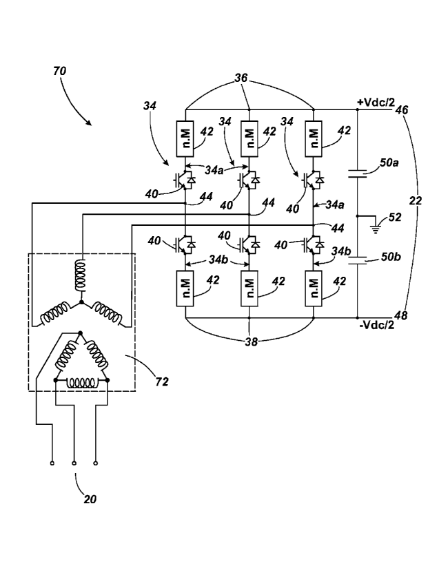
In other embodiments, such as that shown in
Figure 7, the voltage source converter 70 may include
multiple converter limbs 34, each converter limb 34
including an AC terminal 44 for connection to an
individual phase of a multiphase AC network 20. In such
embodiments, the number of converter limbs 34 provided
is dependent on the number of phases of the AC network
20.
The voltage source converter 70 shown in
Figure 7 includes three converter limbs 34 so as to
permit use of the voltage source converter 70 with a
three-phase AC network 20.
CA 02764507 2011-12-05
WO 2010/149200
PCT/EP2009/057736
Each converter limb 34 includes first and
second DC terminals 36,38 and an AC terminal 44. Each
converter limb 34 also defines first and second limb
portions 34a,34b, each limb portion including a
5 switching element 40 connected in series with a chain-
link converter 42 between a respective one of the first
and second DC terminals 36,38 and the AC terminal 44.
The switching element 40 of each of the
10 first and second limb portions 34a,34b is connected to
the AC terminal 44 and the chain-link converter 42 of
each of the first and second limb portions 34a,34b is
connected to the respective DC terminal 36,38.
In use, the terminals 36,38 of each
15 converter limb 34 are connected to the DC network 22
such that the voltage at the first DC terminal 36 of
each converter limb 34 is +VDc/2 and the voltage at the
second DC terminal 38 of each converter limb 34 is -
VDc/2.
20 Each AC terminal 44 is connected to a phase
of the multi-phase AC network 20 via a transformer 72
such that the AC terminals 44 are connected to
respective phases of the AC network 20.
The switching elements 40 of the first and
second limb portions 34a,34b of each converter limb 34
are operable in use to switch the respective chain-link
converters 42 in and out of circuit between the
respective DC terminal and the AC terminal. The chain-
link converters 42 of each converter limb 34 are
operable to generate a voltage waveform at the
CA 02764507 2011-12-05
WO 2010/149200
PCT/EP2009/057736
21
respective AC terminal 44 so that a three-phase voltage
waveform is generated.
Control of the three-phase voltage source
converter is similar to the above-described control of
the single-phase voltage source converter 37 since
operation of the series combination of the switching
element 40 and the chain-link converter 42 in a
converter limb 34 only affects the phase connected to
that converter limb 34, and does not affect the phases
connected to the other converter limbs 34.