Note: Descriptions are shown in the official language in which they were submitted.
CA 02764902 2011-12-08 110283: 910470
DESCRIPTION
TITLE OF INVENTION
Field Effect Transistor
TECHNICAL FIELD
The present invention relates to a field effect transistor, in particular to a
lateral
field-effect transistor.
BACKGROUND ART
As to a lateral field-effect transistor, if an enlarged gate width is used to
increase
current capacity, a comb-shaped structure is often employed for source wiring
and for
drain wiring so that a plurality of transistor cells can be disposed to be
connected in
parallel. In such a case, as for gate wiring, a meander shape or a comb shape
is
employed.
A conventionally proposed field effect transistor has a top surface pattern
formed in such a shape that digitiform portions of comb-shaped source and
drain
electrodes are disposed in opposed positions to interdigitate with each other,
and a
meander-shaped gate electrode is located between the source electrode and the
drain
electrode. Another conventionally proposed field effect transistor has
digitiform
portions of comb-shaped source and drain electrodes formed in an opposing
manner to
interdigitate with each other, digitiform portions of a comb-shaped gate
electrode
formed between the source electrode and the drain electrode, and common
sections to
serve as bases of the digitiform portions of the gate electrode and formed
external to the
transistor (for example, see Japanese Patent Laying-Open No. 2006-066887
(Patent
Literature 1)).
A still another conventionally proposed transistor has a plurality of unit
cells
each having a source contact and a drain contact which are interdigitated, a
gate contact
situated between the source contact and the drain contact, and an overlayer
electrically
coupling the source contact to a p+ region via a p+ contact which is disposed
in a
-1-
CA 02764902 2011-12-08
110283:910470
contact via hole (for example, see International Publication No. WO
2006/065324
(Patent Literature 2)).
CITATION LIST
PATENT LITERATURE
PTL 1: Japanese Patent Laying-Open No. 2006-066887
PTL 2: International Publication No. WO 2006/065324
SUMMARY OF INVENTION
TECHNICAL PROBLEM
Generally, it is understood that on the meander-shaped gate electrode
disclosed
in the document above, there is a gate wiring which is in the same meander
shape as that
of the gate electrode and has one end connected to a gate pad. If the gate
wiring is in a
meander shape, the gate wiring has a high resistance, and charging/discharging
of a gate
circuit takes time. In addition, the gate wiring has a longer length, which
causes a time
lag in a gate voltage change between a section of the gate wiring near the
gate pad and
another section distant from the gate pad. For these reasons, switching of the
transistor cannot be speeded up.
Further, generally, the gate wiring has a width on the order of not more than
I
m. Thus, during a manufacturing process, a missing pattern may occur, where
wiring
is partially not formed due to a failure in photolithography. If the gate
wiring is in a
meander shape, when the gate wiring breaks at even one point, a gate voltage
does not
change in a section of the gate wiring more distant from the gate pad than the
point, and
the transistor does not operate in that section. For this reason, an
operationally
defective transistor product tends to be produced.
Now, the comb-shaped gate wiring disclosed in the above-indicated Japanese
Patent Laying-Open No. 2006-066887 (Patent Literature 1) has the digitiform
portions
of the gate wiring which run below the base of the source wiring. Usually, the
base of
the source wiring takes a large width, and therefore, the gate wiring running
therebelow
has a longer length and a higher resistance. Further, the gate wiring and the
base of the
-2-
CA 02764902 2011-12-08
110283:910470
source wiring have a larger intersecting area between them, which results in a
larger
gate-to-source capacity. For these reasons, charging/discharging of a gate
circuit takes
time, and switching of the transistor cannot be speeded up. In addition, due
to a
missing pattern occurred during a manufacturing process, the digitiform
portions of the
gate wiring break, the transistor does not operate in a section beyond the
broken point,
and an operationally defective transistor product tends to be produced.
The present invention has been made in view of the problems above, and an
object of the invention is to provide a lateral field-effect transistor
capable of improving
switching speed and reducing operationally defective products.
SOLUTION TO PROBLEM
A field effect transistor according to the present invention includes a
substrate,
an active layer formed on the substrate and a source wiring, a drain wiring
and a gate
wiring formed above the active layer. The source wiring is formed in a comb
shape
having a source wiring base and a plurality of source wiring fingers
protruding from the
source wiring base. The drain wiring is formed in a comb shape having a drain
wiring
base and a plurality of drain wiring fingers protruding from the drain wiring
base. The
source wiring and the drain wiring are arranged to oppose each other such that
the
source wiring fingers and the drain wiring fingers interdigitate. The gate
wiring has a
gate wiring base, a plurality of gate wiring fingers protruding from the gate
wiring base,
and a connection connecting tips of adjacent gate wiring fingers. The gate
wiring
finger is arranged between the source wiring finger and the drain wiring
finger, and the
gate wiring base is arranged between the source wiring base and the drain
wiring fingers
and intersects with the source wiring fingers, with an insulating film
interposed between
the gate wiring base and the source wiring fingers.
Preferably, adjacent gate wiring fingers and the connection connecting the
gate
wiring fingers make up a first wiring. A section of the gate wiring base
between two
points where adjacent gate wiring fingers connected by the connection are
connected to
the gate wiring base, respectively, makes up a second wiring which is
electrically parallel
-3-
CA 02764902 2011-12-08
110283:910470
with the first wiring. The first wiring has an electrical resistance not less
than the
electrical resistance of the second wiring.
Preferably, the gate wiring finger has a vertical cross-sectional area not
more
than the vertical cross-sectional area of the gate wiring base.
Preferably, the active layer includes a first conductivity type buffer layer,
a
second conductivity type channel layer formed on the buffer layer and having a
surface,
a second conductivity type source region formed from the surface of the
channel layer
opposing at least part of the source wiring finger to an interior of the
channel layer, a
second conductivity type drain region formed from the surface of the channel
layer
opposing at least part of the drain wiring finger to the interior of the
channel layer, and a
first conductivity type gate region formed from the surface of the channel
layer opposing
at least part of the gate wiring finger to the interior of the channel layer.
The field
effect transistor further includes a source electrode connecting the source
wiring finger
and the source region, a drain electrode connecting the drain wiring finger
and the drain
region, and a gate electrode connecting the gate wiring finger and the gate
region.
Preferably, the active layer includes a first conductivity type buffer layer,
a
second conductivity type channel layer formed on the buffer layer, a first
conductivity
type RESURF layer formed on the channel layer and having a surface, a second
conductivity type source region formed to extend from the surface of the
RESURF layer
opposing at least part of the source wiring finger to the channel layer, a
second
conductivity type drain region formed to extend from the surface of the RESURF
layer
opposing at least part of the drain wiring finger to the channel layer, and a
first
conductivity type gate region formed to extend from the surface of the RESURF
layer
opposing at least part of the gate wiring finger to the channel layer. The
field effect
transistor further includes a source electrode connecting the source wiring
finger and the
source region, a drain electrode connecting the drain wiring finger and the
drain region,
and a gate electrode connecting the gate wiring finger and the gate region.
Preferably, the active layer includes a first conductivity type buffer layer,
a first
-4-
CA 02764902 2011-12-08
110283:910470
conductivity type body layer formed on the buffer layer and having a surface,
a second
conductivity type source region formed from the surface of the body layer
opposing at
least part of the source wiring finger to an interior of the body layer, and a
second
conductivity type drain region formed from the surface of the body layer
opposing at
least part of the drain wiring finger to the interior of the body layer. The
field effect
transistor further includes a gate electrode formed below at least part of the
gate wiring
finger and formed on the body layer, with an insulating layer interposed
therebetween, a
source electrode connecting the source wiring finger and the source region,
and a drain
electrode connecting the drain wiring finger and the drain region.
Preferably, the active layer includes a first conductivity type buffer layer,
a
second conductivity type channel layer formed on the buffer layer and having a
surface,
a second conductivity type source region formed from the surface of the
channel layer
opposing at least part of the source wiring finger to an interior of the
channel layer, and
a second conductivity type drain region formed from the surface of the channel
layer
opposing at least part of the drain wiring finger to the interior of the
channel layer.
The field effect transistor further includes a gate electrode formed below at
least part of
the gate wiring finger, being in contact with the channel layer and exhibiting
the
Schottky characteristics, a source electrode connecting the source wiring
finger and the
source region, and a drain electrode connecting the drain wiring finger and
the drain
region.
Preferably, the field effect transistor further includes a first conductivity
type
base region formed below at least part of the source wiring finger and
extending from
the surface to the buffer layer and a base electrode connecting the source
wiring finger
and the base region.
Preferably, the base region is surrounded by the source region when the field
effect transistor is seen in plan view.
Preferably, the base electrode is provided below the source electrode.
ADVANTAGEOUS EFFECTS OF INVENTION
-5-
CA 02764902 2011-12-08
110283:910470
According to a field-effect transistor of the present invention, improved
switching speed and reduced operationally defective products can be achieved.
BRIEF DESCRIPTION OF DRAWINGS
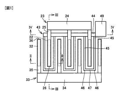
Fig. 1 is a schematic diagram showing a wiring shape of a lateral field-effect
transistor of a first embodiment.
Fig. 2 is a cross-sectional view of the lateral field-effect transistor of the
first
embodiment.
Fig. 3 is another cross-sectional view of the lateral field-effect transistor
of the
first embodiment.
Fig. 4 is still another cross-sectional view of the lateral field-effect
transistor of
the first embodiment.
Fig. 5 is an exploded view of part of a gate wiring.
Fig. 6 is a cross-sectional view along a line VI-VI in Fig. 5 of a base of the
gate
wiring.
Fig. 7 is a cross-sectional view along a line VII-VII in Fig. 5 of a finger of
the
gate wiring.
Fig. 8 is a flowchart showing a method for manufacturing the lateral field-
effect
transistor of the first embodiment.
Fig. 9 is a cross-sectional view of a lateral field-effect transistor of a
second
embodiment.
Fig. 10 is a cross-sectional view of a lateral field-effect transistor of a
third
embodiment.
Fig. 11 is a cross-sectional view of a lateral field-effect transistor of a
fourth
embodiment.
Fig. 12 is a cross-sectional view of a lateral field-effect transistor of a
fifth
embodiment.
Fig. 13 is a cross-sectional view of a lateral field-effect transistor of a
sixth
embodiment.
-6-
CA 02764902 2011-12-08
110283:910470
DESCRIPTION OF EMBODIMENTS
Embodiments of the present invention will be described hereinafter with
reference to the drawings. In the drawings below, the same or corresponding
elements
have the same reference characters allotted, and description thereof will not
be repeated.
First Embodiment
Fig. I is a schematic diagram showing a wiring shape of a lateral field-effect
transistor of a first embodiment. Fig. I illustrates an arrangement of source
wiring,
drain wiring and gate wiring of the lateral field-effect transistor. As shown
in Fig. 1,
the lateral field-effect transistor of the present embodiment includes source
wiring 23,
drain wiring 33 and gate wiring 43. Source wiring 23 is formed in a comb shape
having a base 24 and a plurality of fingers 25 protruding from base 24. A
plurality of
fingers 25 of source wiring 23 are each connected to base 24. Drain wiring 33
is
formed in a comb shape having a base 34 and a plurality of fingers 35
protruding from
base 34. A plurality of fingers 35 of drain wiring 33 are each connected to
base 34.
Source wiring 23 and drain wiring 33 are arranged to oppose each other such
that fingers 25 of comb-shaped source wiring 23 and fingers 35 of comb-shaped
drain
wiring 33 interdigitate. That is, source wiring 23 and drain wiring 33 are
arranged
such that fingers 25 of source wiring 23 and fingers 35 of drain wiring 33 are
arranged
alternately.
Source wiring 23 shown in Fig. 1 has three fingers 25. Fingers 25 protrude
from one side of base 24 in a manner orthogonal to base 24. Drain wiring 33
shown in
Fig. 1 has four fingers 35. Fingers 35 protrude from one side of base 34 in a
manner
orthogonal to base 24. Source wiring 23 and drain wiring 33 are arranged such
that
three fingers 25 of source wiring 23 are inserted between four fingers 3 5 of
drain wiring
33.
Base 24 of source wiring 23 and base 34 of drain wiring 33 are arranged in
parallel to each other. Fingers 25 of source wiring 23 extend from base 24
toward base
34 of drain wiring 33. Fingers 35 of drain wiring 33 extend from base 34
toward base
-7-
CA 02764902 2011-12-08
110283:910470
24 of source wiring 23. Fingers 25 of source wiring 23 and fingers 35 of drain
wiring
33 are disposed in parallel to each other and arranged one by one alternately.
Below the portions of fingers 25 of source wiring 23 disposed being
interdigitated with fingers 35 of drain wiring 33, source electrodes 22 shown
in Fig. I in
a dotted line are arranged. Below the portions of fingers 35 of drain wiring
33
disposed being interdigitated with fingers 25 of source wiring 23, drain
electrodes 32
shown in Fig. I in a dotted line are arranged. "Above" herein indicates
farther away
from a substrate in a depositional direction of a semiconductor, while "below"
indicates
closer to the substrate in the depositional direction of the semiconductor.
Gate wiring 43 has a base 44 and a plurality of fingers 45 protruding from
base
44. When the transistor is seen in plan view, on the side in the vicinity of
base 24 of
source wiring 23, base 44 of gate wiring 43 is arranged. Base 44 of gate
wiring 43 is
arranged between base 24 of source wiring 23 and fingers 35 of drain wiring
33. Base
44 of gate wiring 43 is arranged below fingers 25 of source wiring 23 and
intersects
with fingers 25 of source wiring 23, with an insulating film interposed
therebetween.
Base 44 of gate wiring 43 has one end connected to a gate pad 49 formed of a
conductive material such as metal.
Fingers 45 of gate wiring 43 protrude from one side of base 44 in a manner
orthogonal to base 44. The plurality of fingers 45 of gate wiring 43 are
arranged in
parallel to each other. Finger 45 of gate wiring 43 is arranged between finger
25 of
source wiring 23 and finger 35 of drain wiring 33. Fingers 45 of gate wiring
43 extend
from base 44 toward base 34 of drain wiring 33. Fingers 45 of gate wiring 43,
fingers
of source wiring 23 and fingers 35 of drain wiring 33 are disposed in parallel
to each
other.
25 Gate wiring 43 further has a connection 47 connecting tips 46 of adjacent
fingers
45. Tips 46 of a pair of adjacent fingers 45 on the side along base 34 of
drain wiring
33 are connected to each other by connection 47. As to fingers 45 of gate
wiring 43,
adjacent ones are connected on their distal ends to each other by connection
47, with
-8-
CA 02764902 2011-12-08
110283:910470
finger 25 of source wiring 23 sandwiched therebetween. Fingers 45 and
connection 47
of gate wiring 43 are formed in a U-shape surrounding finger 25 of source
wiring 23.
Fig. 2 is a cross-sectional view of the lateral field-effect transistor of the
first
embodiment. Fig. 2 illustrates a cross section along a line II-II in Fig. I of
a lateral
RESURF-JFET (REduced SURface Field Junction Field Effect Transistor) I to
serve as
an example of the lateral field-effect transistor.
In RESURF-JFET 1 shown in Fig. 2, an active layer 14 made of a
semiconductor is formed on a substrate 10 formed of a semiconductor such as
SiC.
RESURF-JFET I has substrate 10 and active layer 14 formed on substrate 10.
Source
wiring 23, drain wiring 33 and gate wiring 43 are formed above active layer
14.
Active layer 14 includes a p- type buffer layer 1 I formed on substrate 10, an
n
type channel layer 12 formed on buffer layer 11 and a p type RESURF layer 13
formed
on channel layer 12. RESURF layer 13 has a surface 13a. An n+ type source
region
21, an n+ type drain region 3 1 and a p+ type gate region 41 are formed at a
distance
from each other and in a manner extending from surface 13a of RESURF layer 13
to
channel layer 12.
Buffer layer 11, RESURF layer 13 and gate region 41 have p type conductivity
as a first conductivity type. Gate region 41 has a higher p type impurity
concentration
than the p type impurity concentration in RESURF layer 13. Buffer layer 1 I
has a
lower p type impurity concentration than the p type impurity concentration in
RESURF
layer 13. Channel layer 12, source region 21 and drain region 31 have n type
conductivity as a second conductivity type. Source region 21 and drain region
31 have
a higher n type impurity concentration than the n type impurity concentration
in channel
layer 12.
On surface 13a to serve as an upper surface of RESURF layer 13, a field oxide
film 20 made of an insulating material is formed. In field oxide film 20, a
plurality of
openings are formed. In the opening located on source region 21, source
electrode 22
is formed. In the opening located on drain region 31, drain electrode 32 is
formed. In
-9-
CA 02764902 2011-12-08
110283:910470
the opening located on gate region 41, gate electrode 42 is formed.
Field oxide film 20 is formed to cover the entire region on surface 13a of
RESURF layer 13 except the region where source electrode 22, drain electrode
32 and
gate electrode 42 are formed. This results in that field oxide film 20
electrically isolates
each of source electrode 22, drain electrode 32 and gate electrode 42.
Source region 21 to which electrons are supplied is formed to oppose finger 25
of source wiring 23. On source electrode 22 above source region 21, source
wiring 23
made of a conductive material such as metal is formed. Source electrode 22
electrically connects finger 25 of source wiring 23 and source region 21.
Drain region 31 from which electrons are drawn is formed to oppose finger 35
of
drain wiring 33. On drain electrode 32 above drain region 31, drain wiring 33
made of
a conductive material is formed. Drain electrode 32 electrically connects
finger 35 of
drain wiring 33 and drain region 3 1.
Gate region 41 which is arranged between source region 21 and drain region 31
and establishes and interrupts an electrical connection between source region
21 and
drain region 31 is formed to oppose finger 45 of gate wiring 43. On gate
electrode 42
above gate region 41, gate wiring 43 made of a conductive material is formed.
Gate
electrode 42 electrically connects finger 45 of gate wiring 43 and gate region
41.
On field oxide film 20, an interlayer insulating film 51 is formed. Interlayer
insulating film 51 is formed to cover gate wiring 43 and to fill between
source wiring 23
and drain wiring 33. Interlayer insulating film 51 electrically insulates
between source
wiring 23 and gate wiring 43 and electrically insulates between drain wiring
33 and gate
wiring 43.
On interlayer insulating film 51, a passivation film 52 is formed. Passivation
film 52 is formed to cover entire RESURF-JFET 1, including entire source
wiring 23
and drain wiring 33. Passivation film 52 operates as a surface protective film
which
externally protects RESURF-JFET 1.
Fig. 3 is another cross-sectional view of the lateral field-effect transistor
of the
-10-
CA 02764902 2011-12-08
110283:910470
first embodiment. Fig. 3 illustrates a cross section along a line 111-111 in
Fig. I of
RESURF-JFET 1. Fig. 3 illustrates base 44 and connection 47 of gate wiring 43.
Below base 44 and connection 47, gate region 41 is formed. Base 44 and
connection
47 of gate wiring 43 are each connected to gate region 41 via gate electrode
42.
Between base 44 and connection 47 of gate wiring 43, finger 25 of source
wiring
23 is provided. Below finger 25 of source wiring 23, source region 21 is
formed. On
a left end of source wiring 23 shown in Fig. 3, base 24 of source wiring 23 is
arranged.
In Fig. 3, finger 25 of source wiring 23 extends from above gate region 41 to
a position
to cover base 44 of gate wiring 43, in the lateral direction in the drawing.
Base 44 of
gate wiring 43 intersects with a portion of finger 25 of source wiring 23
closest to base
24, with interlayer insulating film 51 interposed between base 44 of gate
wiring 43 and
finger 25 of source wiring 23.
Fig. 3 illustrates base 34 of drain wiring 33. Drain electrode 32 is arranged
below finger 35 of drain wiring 33 as described with reference to Fig. 1,
however, not
arranged below base 34 of drain wiring 33. Thus, in Fig. 3, drain electrode 32
and
drain region 31 are not arranged below drain wiring 33.
Fig. 4 is still another cross-sectional view of the lateral field-effect
transistor of
the first embodiment. Fig. 4 illustrates a cross section along a line IV-IV in
Fig. I of
RESURF-JFET 1. Fig. 4 illustrates base 44 of gate wiring 43 extending in the
lateral
direction in the drawing. Below base 44, gate region 41 is formed. Base 44 of
gate
wiring 43 is connected to gate region 41 via gate electrode 42.
Base 44 of gate wiring 43 is covered with interlayer insulating film 51. On
interlayer insulating film 51, fingers 25 of source wiring 23 are arranged to
be covered
with passivation film 52. That is, as is clear from Figs. 3 and 4, interlayer
insulating
film 51 is interposed between fingers 25 of source wiring 23 and base 44 of
gate wiring
43. This electrically isolates between fingers 25 of source wiring 23 and base
44 of
gate wiring 43.
One end of base 44 of gate wiring 43 is connected to gate pad 49. Gate pad 49
-11-
CA 02764902 2011-12-08
110283:910470
extends from the top of field oxide film 20 through interlayer insulating film
51 and
passivation film 52 in the thickness direction to be exposed on an outer
surface of
RESURF-JFET 1. Electrical connection between an external electrical circuit
and gate
wiring 43 is made possible via gate pad 49 arranged in this way.
Fig. 5 is an exploded view of part of gate wiring 43. Fig. 5 shows a pair of
adjacent fingers 45 of gate wiring 43 and connection 47 connecting fingers 45,
which
make up first wiring 101. First wiring 101 has a U-shaped structure formed by
base 44
and connection 47 of gate wiring 43. The section of base 44 of gate wiring 43
between
two points where adjacent fingers 45 connected by connection 47 are connected
to base
44 makes up second wiring 102 which is electrically parallel with first wiring
101.
Second wiring 102 is a portion of base 44 which connects two points of base 44
corresponding to positions to which two points on the tip ends of the U-shaped
structure of first wiring 101 are connected. U-shaped first wiring 101 and
linear
second wiring 102 are electrically parallel to each other.
Gate wiring 43 is formed such that first wiring 101 has an electrical
resistance
not less than the electrical resistance of second wiring 102. Relative to the
electrical
resistance of a conductive path formed by fingers 45 and connection 47 of gate
wiring
43 arranged in a U-shape, a portion of base 44 of gate wiring 43 in parallel
with the
conductive path has an equal or less electrical resistance. For this reason,
current flows
more easily through second wiring 102 than through first wiring 101. That is,
when a
voltage is applied to base 44 forming second wiring 102, current flowing
through an
interior of base 44 is larger than current which is indicated by an arrow in
Fig. 5 and
flows from finger 45 on the right in the drawing by way of connection 47 to
finger 45 on
the left.
Fig. 6 is a cross-sectional view along a line VI-VI in Fig. 5 of base 44 of
gate
wiring 43. Fig. 7 is a cross-sectional view along a line VII-VII in Fig. 5 of
finger 45 of
gate wiring 43. Comparing Fig. 6 and Fig. 7, finger 45 of gate wiring 43 has a
vertical
cross-sectional area not more than the vertical cross-sectional area of base
44 of gate
-12-
CA 02764902 2011-12-08
110283:910470
wiring 43. Here, "vertical cross-sectional area" refers to the cross-sectional
area of
wiring when cut at right angle to a direction in which the wiring extends.
For example, base 44 of gate wiring 43 may have a width wl of 5 m and a
thickness hl of 0.1 m. The length of base 44 forming second wiring 102 to be
in
parallel with U-shaped first wiring 101 may be 10 m. Further, finger 45 of
gate
wiring 43 may have a width w2 of 2 m and a thickness h2 of 0.1 m, and finger
45 may
have a length of 150 m.
In RESURF-JFET 1 having the configuration above, a plurality of fingers 45 are
formed in a manner protruding from base 44 of gate wiring 43, and a plurality
of fingers
45 are connected to base 44 in parallel. For this reason, as compared with
conventional meander-shaped gate wiring, a difference between electrical
resistances of
a path from gate pad 49 to finger 45 close to gate pad 49 and a path to finger
45 distant
from gate pad 49 can be made smaller. Therefore, a time lag in gate voltage
change
between finger 45 close to gate pad 49 and finger 45 away from gate pad 49 can
be
made small.
Gate wiring 43 is formed such that the electrical resistance of first wiring
101
formed by fingers 45 and connection 47 of gate wiring 43 is not less than the
electrical
resistance of second wiring 102 formed by base 44 and in parallel with first
wiring 101.
Since the electrical resistance in base 44 of gate wiring 43 is small, the
resistance to
current flowing through base 44 can be made small. At the same time, since
current
flows through base 44 more easily as compared with finger 45, a time lag in
gate voltage
change between finger 45 close to gate pad 49 and finger 45 distant from gate
pad 49
can be made smaller. By making the vertical cross-sectional area of finger 45
of gate
wiring 43 not more than the vertical cross-sectional area of base 44, a more
remarkable
effect of achieving a smaller resistance of base 44 as compared with finger 45
can be
obtained.
Further, since base 44 of gate wiring 43 is arranged between base 24 of source
wiring 23 and drain wiring 33, source wiring 23 and gate wiring 43 have
smaller
-13-
CA 02764902 2011-12-08
110283:910470
intersecting area therebetween. Generally, base 24 of source wiring 23 has a
larger
width (the size in a direction orthogonal to a direction in which base 24
extends (the
vertical direction in Fig. 1) than the width of base 44 of gate wiring 43. For
this reason,
as compared with the intersecting area between a base of source wiring and
fingers of
gate wiring in the conventional art where fingers of the comb-shaped gate
wiring run
below the base of the source wiring, the intersecting area between fingers 25
of source
wiring 23 and base 44 of gate wiring 43 in the configuration of the present
embodiment
can be made smaller. Accordingly, a smaller gate-to-source capacity can be
achieved,
and therefore, time required for charging/discharging a gate circuit can be
shortened.
As such, RESURF-JFET 1 of the present embodiment has a smaller time lag in a
gate voltage change and a shorter time required for charging/discharging a
gate circuit,
and therefore, an improved switching speed of RESURF-JFET I can be achieved.
At the same time, in RESURF-JFET I of the present embodiment, since a
plurality of fingers 45 are connected in parallel to base 44 of gate wiring
43, a missing
pattern occurred in one finger 45 does not affect transmission of a gate
voltage change
to other fingers 45. Further, since two adjacent fingers 45 and connection 47
form U-
shaped wiring which has two connection points to base 44, even if a missing
pattern
occurs at one point on finger 45 and the wiring breaks, it is possible to
transmit a gate
voltage change to a portion of wiring ahead thereof, from the other connection
with
base 44, thereby to operate the transistor. In a case where two or more points
within
one U-shaped wiring break, although a portion where transistor does not
operate is
created, there is no effect on transmission of a gate voltage change to other
fingers 45 in
this case as well. Occurrence of an operationally defective transistor product
can
therefore be suppressed.
A missing pattern could also occur in base 44 of gate wiring 43. However, by
making the vertical cross-sectional area of finger 45 of gate wiring 43 not
more than the
vertical cross-sectional area of base 44, it is possible to reduce the
possibility that the
missing pattern causes gate wiring 43 to break in base 44, as compared with
finger 45.
-14-
CA 02764902 2011-12-08 110283:910470
Occurrence of an operationally defective transistor product can therefore be
further
suppressed.
Next, a method for manufacturing RESURF-JFET I shown in Figs. 2 to 4 will
be described. Fig. 8 is a flow chart showing a method for manufacturing the
lateral
field-effect transistor of the first embodiment. In a method for manufacturing
RESURF-JFET I implementing the lateral field-effect transistor according to
the present
embodiment, the following steps are performed.
First, substrate 10 to serve as a semiconductor substrate is prepared (S 10).
For
example, an n type substrate of such as single crystal type SiC called 4H-SiC
is prepared.
Buffer layer 11 which is located on a main surface of substrate 10 and made of
an SiC
layer including a p type impurity as a first conductivity type impurity is
then formed
(S20). Buffer layer 11 can have a thickness of 10 m, for example, and an
epitaxial
growth method can be used as a film forming method. Aluminum (Al) may be used
as
a p type impurity. Buffer layer 11 has a p type impurity concentration of, for
example,
1.0X 10', cm-1.
Channel layer 12 located on buffer layer 11 and including a second
conductivity
type (n type) impurity having a higher concentration than the concentration of
the p type
impurity in buffer layer 11 is then formed (S30). Nitrogen (N) may be used as
an n
type impurity. Channel layer 12 may have a thickness of 0.4 m, for example.
Channel layer 12 may have a concentration of the n type conductive impurity of
2.0X 10" cm 3. Subsequently RESURF layer 13 is formed on channel layer 12
(S40).
RESURF layer 13 includes a first conductivity type (p type) impurity having a
higher
concentration than the concentration of the p type impurity in buffer layer
11.
RESURF layer 13 may have a thickness of, for example, 0.25 urn and RESURF
layer 13
may have a p type conductive-impurity concentration of 2.0X 1017 cm 3.
Gate region 41 including a first conductivity type (p type) impurity is then
formed to extend from surface 13a of RESURF layer 13 through RESURF layer 13
to
channel layer 12 (S50). Specifically, a patterned resist film is formed using
a
- 15 -
CA 02764902 2011-12-08
110283:910470
photolithography method. By means of the resist film as a mask, aluminum (Al)
is
implanted into RESURF layer 13 and channel layer 12 using an ion implantation
method.
In this way, gate region 41 of p type conductivity is formed. Gate region 41
may have
a depth of, for example, 0.4 m. Further, gate region 41 may have a p type
impurity
concentration of, for example, I.OX 1019 cm 3.
Source region 21 and drain region 31 opposing each other with gate region 41
sandwiched therebetween and including a second conductivity type (n type)
impurity are
then formed to extend from surface 13a of RESURF layer 13 through RESURF layer
13
to channel layer 12 (S60). Specifically, as in the above-described step for
forming gate
region 41, source region 21 and drain region 31 of n type conductivity are
formed by
implanting phosphorus (P) into RESURF layer 13 and channel layer 12 using an
ion
implantation method. Source region 21 and drain region 31 may have a depth of
0.4
m, for example. Source region 21 and drain region 31 may have an n type
impurity
concentration of, for example, 5.Ox 10i9 cm-'.
Activation annealing for activating ions implanted into the above-described
gate
region 41, source region 21, and drain region 31 is then performed (S70). As
to
conditions for the activation-annealing step, for example, argon gas may be
used as an
ambient, and a heating temperature of 1700 C and a heating time of 30 minutes
may be
employed. It is noted that the ambient pressure in annealing may be 100 kPa,
for
example. Field oxide film 20 is then formed (S80). Specifically, surface 13a
of
RESURF layer 13 is thermally oxidized to form field oxide film 20 by heating,
in an
oxygen atmosphere, substrate 10 which has been subjected to the above-
described
processes. As to heating conditions, for example, a heating temperature of
1300 C and
a heating time of 60 minutes may be employed. It is noted that the ambient
pressure in
heating may be at the atmospheric pressure. As a result, field oxide film 20
having a
thickness of 0.1 m is formed.
An opening is then formed in a predetermined region of field oxide film 20
(S90),
The opening is formed at a position where an electrode is formed in a
subsequent step.
- 16-
CA 02764902 2011-12-08
110283:910470
Specifically, a resist film having a predetermined pattern is formed on field
oxide film 20
using a photolithography method. This resist film has an opening pattern
formed in a
region in which opening is to be formed. Using this resist film as a mask,
field oxide
film 20 is partially removed by etching. In this way, the opening is formed.
An ohmic electrode is then formed within the opening (S 100). Specifically, a
conductive material film (for example, a nickel (Ni) film) constituting the
ohmic
electrode is formed within the opening and on the upper surface of the resist
film using a
vapor deposition method. Subsequently, by removing the resist film, a portion
of the
Ni film formed on the resist film is also removed (lift-off procedure). Then,
in an argon
atmosphere, the SiC substrate on which the Ni film has been formed is heat-
treated and
the Ni film is turned into the ohmic electrode. As to the conditions for this
heat
treatment, for example, a heating temperature of 950 C and a heating time of 2
minutes
may be employed. Further, the pressure of the argon atmosphere may be at the
atmospheric pressure. In this way, source electrode 22 in contact with source
region
21, drain electrode 32 in contact with drain region 31, and gate electrode 42
in contact
with gate region 41 are formed.
Gate wiring 43 is then formed on gate electrode 42 (S 110). Specifically, a
patterned resist film is formed on gate electrode 42 using a photolithography
method.
The resist film has an opening pattern formed to expose gate electrode 42. A
conductive material film (for example, an aluminum film) to turn into gate
wiring 43 is
formed by vapor deposition onto the interior of the opening pattern of the
resist film.
The aluminum film may have a thickness of 0.1 m, for example. Subsequently,
part of
the conductive material film located on the resist film is removed by removing
the resist
film (lift-off procedure). As a result, gate wiring 43 located on gate
electrode 42 is
obtained.
Interlayer insulating film 51 covering gate wiring 43 is then formed (S 120).
Specifically, a plasma CVD (Chemical Vapor Deposition) method is used to form
interlayer insulating film 51 made of an Si02 film having a thickness of 0.2
m. In this
-17-
CA 02764902 2011-12-08
110283:910470
way, interlayer insulating film 51 is formed to be in contact with the
surfaces of gate
wiring 43, source electrode 22, drain electrode 32, and field oxide film 20.
Part of interlayer insulating film 51 is then removed to form openings in
predetermined regions of interlayer insulating film 51 (S 130). The openings
are formed
at positions where gate pad 49, source wiring 23 and drain wiring 33 are to be
formed in
a subsequent step. Specifically, after a resist is applied onto interlayer
insulating film
51, exposure and development are performed, and a resist film having an
opening in a
desired region of interlayer insulating film 51 is formed. The resist film is
used as a
mask to partially remove interlayer insulating film 51, for example, by RIE
(Reactive Ion
Etching). In this way, interlayer insulating film 51 in contact with source
electrode 22
and drain electrode 32 is removed, and interlayer insulating film 51 in a
region
corresponding to the arrangement of gate pad 49 is removed as well.
Source wiring 23 including a pad, drain wiring 33 including a pad and gate pad
49 are then formed (S 140). Specifically, on interlayer insulating film 51
partially
removed by RIE, an aluminum film made of aluminum and having a thickness of 3
pm is
formed by, for example, spattering and etched into a desired shape, so that
source wiring
23, drain wiring 33 and gate pad 49 are formed.
Passivation film 52 is then formed (S150). Specifically, on the entire top
surface of RESURF-JFET 1 except a pad portion such as gate pad 49 to be
externally
connected, for example, on the surface of interlayer insulating film 51 and
above source
wiring 23 and drain wiring 33 formed in step (S140), passivation film 52 made
of an
S102 film having a thickness of 5 m is formed by, for example, plasma CVD. By
forming passivation film 52 to serve as a protection film, RESURF-JFET 1 is
externally
protected.
Such a manufacturing method can readily provide RESURF-JFET I capable of
improving the switching speed and reducing operationally defective products,
as shown
in Figs. 2 to 4.
Second Embodiment
-18-
CA 02764902 2011-12-08
110283:910470
Fig. 9 is a cross-sectional view of a lateral field-effect transistor of a
second
embodiment. The lateral RESURF-JFET I shown in Fig. 9 to serve as an example
of
the lateral field-effect transistor has the same basic configuration as that
of RESURF-
JFET I of the first embodiment. RESURF-JFET I of the second embodiment is,
however, different from RESURF-JFET I of the first embodiment in that a base
region
61 electrically in contact with buffer layer 11 is formed.
Specifically, RESURF-JFET I of the second embodiment includes p+ type base
region 61 which is formed below part of finger 25 of source wiring 23. Base
region 61
is formed to extend from surface 13a of RESURF layer 13 to buffer layer 11. On
base
region 61, a base electrode 62 which is in contact with base region 61 is
formed. Base
electrode 62 connects finger 25 of source wiring 23 and base region 61. Base
electrode 62 is electrically in contact with buffer layer 11. Base electrode
62 is
arranged to be in contact with source electrode 22 and has the same electric
potential as
that of source electrode 22.
Although base electrode 62 can be placed at any place as long as a connection
with source wiring 23 can be made, it is desirable that the electrode be
provided under
finger 25 of source wiring 23 together with source electrode 22. Fig. 9
illustrates a
cross section ofRESURF-JFET 1, however, it is more preferable that base
electrode 62
be surrounded by source electrode 22 in plan view. That is, it is more
preferable that
base region 61 be surrounded by source region 21 when RESURF-JFET 1 is seen in
plan view.
In RESURF-JFET 1 of the second embodiment having such a configuration,
since base electrode 62 is provided below finger 25 of source wiring 23
together with
source electrode 22, stabilization of operation of a transistor cell is
promoted. Further,
extension of a depletion layer in an OFF operation of the transistor and
contraction of
the depletion layer in an ON operation within buffer layer 11 are promoted.
Therefore,
an improved switching speed of RESURF-JFET I can be achieved. Base region 61
surrounded by source region 21 in plan view can provide a more stable
operation of the
-19-
CA 02764902 2011-12-08
110283:910470
transistor.
A method for manufacturing RESURF-JFET I shown in Fig. 9 is basically the
same as the method for manufacturing RESURF-JFET I of the first embodiment
basically shown in Fig. 8, however, different in that the step of forming base
region 61 is
added. Specifically, steps (S 10) to (S60) shown in Fig. 8 are performed.
Subsequently, aluminum ion implantation is performed with a depth reaching
buffer
layer 11 to form p+ type base region 61. Base region 61 may have a depth of
0.9 pm,
for example. Base region 61 may have a p type impurity concentration of, for
example,
1.0X1019 cm3.
Activation annealing for activating ions implanted into base region 61
simultaneously with gate region 41, source region 21 and drain region 31 is
then
performed in step (S70). Subsequently, steps (S80) to (S90) are performed, and
in
step (S 100), an ohmic electrode is formed integrated with source electrode 22
and on
base region 61 so as to form base electrode 62. Subsequently, steps (S I10) to
(S 150)
are performed. In this way, RESURF-JFET I including base region 61 shown in
Fig. 9
can be obtained.
Third Embodiment
Fig. 10 is a cross-sectional view of a lateral field-effect transistor of a
third
embodiment. The lateral RESURF-JFET 1 shown in Fig. 10 to serve as an example
of
the lateral field-effect transistor has the same basic configuration as that
of RESURF-
JFET I of the second embodiment shown in Fig. 9. RESURF-JFET I of the third
embodiment is, however, different from RESURF-JFET 1 of the first embodiment
in
that base electrode 62 is provided below source electrode 22.
In RESURF-JFET 1 of the third embodiment, a trench engraved from surface
13a of RESURF layer 13 toward buffer layer 1I is formed. Base region 61 is
formed
below the trench. Base electrode 62 is provided at the bottom of the trench so
as to be
in contact with base region 61. Asa result, base electrode 62 is formed below
source
electrode 22 surrounding base electrode 62 in plan view, namely, formed in
more
-20-
CA 02764902 2011-12-08 110283:910470
proximity to buffer layer 11 than the source electrode.
In RESURF-JFET I of the third embodiment having such a configuration, base
region 61 including a p type impurity can be formed by forming a trench
engraved from
surface 13a of RESURF layer 13 and performing ion implantation into the bottom
of the
trench. That is, there is no need to perform deep ion implantation from
surface 13a of
RESURF layer 13 toward buffer layer 11 in order to form base region 61.
Therefore, a
simpler and easier process of manufacturing RESURF-JFET I can be achieved.
A method for manufacturing RESURF-JFET I shown in Fig. 10 is basically the
same as the method for manufacturing RESURF-JFET I of the first embodiment
basically shown in Fig. 8, however, different in that the step of forming a
trench in
RESURF layer 13 and forming base region 61 thereafter is added. Specifically,
steps
(S 10) to (S40) shown in Fig. 8 are performed. Subsequently, a trench is
formed by
RIE in a region corresponding to a place where base region 61 is to be formed.
The
depth of the trench is determined to be to such an extent that when ion
implantation of a
p type impurity into the bottom of the trench is performed with the same
implantation
depth as that of gate region 41, the region subjected to the ion implantation
reaches
buffer layer 11. For example, the trench may have a depth of 0.5 m.
Next, in step (S50), simultaneously with ion implantation for forming gate
region
41, aluminum ion implantation is performed from the bottom of the trench
formed in the
previous step. This forms, below the trench, base region 61 including the p
type
impurity. Base region 61 may have a depth of 0.4 m, for example. Further,
base
region 61 may have a p type impurity concentration of, for example, 1.OX 10'9
cm-3.
Then, step (S60) is performed, followed by step (S70) in which activation
annealing for activating ions implanted into base region 61 simultaneously
with gate
region 41, source region 21 and drain region 31 is performed. Subsequently,
steps
(S80) to (S90) are performed, and in step (S 100), simultaneously with the
formation of
source electrode 22, drain electrode 32 and gate electrode 42, an ohmic
electrode is
formed on base region 61 to form base electrode 62. Subsequently, steps (S I
10) to
-21 -
CA 02764902 2011-12-08
110283:910470
(S 150) are performed. In this way, RESURF-JFET I shown in Fig. 10 and having
base
electrode 62 provided below source electrode 22 can be obtained.
Fourth Embodiment
Fig. 11 is a cross-sectional view of a lateral field-effect transistor of a
fourth
embodiment. The lateral JFET 71 shown in Fig. 11 to serve as an example of the
lateral field-effect transistor has the same basic configuration as that of
RESURF-JFET
1 of the first embodiment. JFET 71 is, however, different from RESURF-JFET I
of
the first embodiment in that no RESURF layer is formed on channel layer 12 and
in that
channel layer 12 is formed also in a region where RESURF layer 13 is formed in
RESURF-JFET 1 shown in Fig. 2.
Specifically, in JFET 71 shown in Fig. 11, active layer 14 includes p- type
buffer
layer 11 formed on substrate 10 and n type channel layer 12 formed on buffer
layer I I .
Channel layer 12 has a surface 12a. From surface 12a of channel layer 12 to
the
interior of channel layer 12, n+ type source region 21, n+ type drain region
31 and p+
type gate region 41 are formed. In field oxide film 20 formed on surface 12a
to serve
as an upper surface of channel layer 12, a plurality of openings are formed.
Within the opening located on source region 21, source electrode 22 is formed.
Source region 21 is formed to oppose finger 25 of source wiring 23. Source
electrode
22 electrically connects finger 25 of source wiring 23 and source region 21.
Within the opening located on drain region 31, drain electrode 32 is formed.
Drain region 31 is formed to oppose finger 35 of drain wiring 33. Drain
electrode 32
electrically connects finger 35 of drain wiring 33 and drain region 31.
Within the opening located on gate region 41, gate electrode 42 is formed.
Gate region 41 is formed to oppose finger 45 of gate wiring 43. Gate electrode
42
electrically connects finger 45 of gate wiring 43 and gate region 41.
Also in JFET 71 having the configuration above, base 44 of gate wiring 43 is
arranged between base 24 of source wiring 23 and drain wiring 33, and base 44
of gate
wiring 43 and fingers 25 of source wiring 23 intersect with each other. For
this reason,
-22-
CA 02764902 2011-12-08
110283 910470
as in RESURF-JFET I of the first embodiment, a time lag in gate voltage change
is
smaller, and time required for charging/discharging a gate circuit is
shortened, and
therefore, an improved switching speed of JFET 71 can be achieved.
Furthermore,
occurrence of an operationally defective transistor product can be suppressed.
A method for manufacturing JFET I shown in Fig. 11 is basically the same as
the
method for manufacturing RESURF-JFET I of the first embodiment basically shown
in
Fig. 8, however, different in that step (S40) of forming RESURF layer 13 is
not
performed. Specifically, steps (S 10) to (S20) shown in Fig. 8 are performed.
Subsequently, on buffer layer 11, channel layer 12 is formed (S30). Channel
layer 12
may have a thickness of 0.65 gm, for example. At surface 12a of channel layer
12,
gate region 41 including a first conductivity type (p type) impurity is formed
(S50).
At surface 12a of channel layer 12, source region 21 and drain region 31 which
include a second conductivity type (n type) impurity are then formed to oppose
each
other, with gate region 41 sandwiched therebetween (S60). This is followed by
activation annealing for activating ions implanted into gate region 41, source
region 21
and drain region 31 (S70). Surface 12a of channel layer 12 is then thermally
oxidized
to form field oxide film 20 (S80). Subsequently, steps (S90) to (S 150) are
performed.
In this way, JFET 71 shown in Fig. II can be obtained.
Fifth Embodiment
Fig. 12 is a cross-sectional view of a lateral field-effect transistor of a
fifth
embodiment. The lateral MOSFET (Metal-Oxide-Semiconductor Field-Effect
Transistor) 81 shown in Fig. 12 to serve as an example of lateral field-effect
transistor
has the same basic configuration as that of RESURF-JFET 1 of the first
embodiment.
In MOSFET 71, however, a p type body layer 82 is formed on buffer layer 11,
and
source region 21, drain region 31 and an n type drift layer 83 are formed
within body
layer 82, whereas gate region 41 shown in Fig. 2 is not formed. Gate electrode
42 is
formed on field oxide film 20.
More specifically, in MOSFET 81 shown in Fig. 12, active layer 14 includes p-
-23-
CA 02764902 2011-12-08
110283:910470
type buffer layer 11 formed on substrate 10 and p type body layer 82 formed on
buffer
layer 11. Body layer 82 has a surface 82a. From surface 82a of body layer 82
to the
interior of body layer 82, n+ type source region 21 and n+ type drain region
31 are
formed. In field oxide film 20 formed on surface 82a to serve as an upper
surface of
body layer 82, a plurality of openings are formed.
Within the opening located on source region 21, source electrode 22 is formed.
Source region 21 is formed to oppose finger 25 of source wiring 23. Source
electrode
22 is in contact with source region 21 and electrically connects finger 25 of
source
wiring 23 and source region 21.
Within the opening located on drain region 31, drain electrode 32 is formed.
Drain region 31 is formed to oppose finger 35 of drain wiring 33. Drain
electrode 32 is
in contact with drain region 31 and electrically connects finger 35 of drain
wiring 33 and
drain region 3 1.
N type drift layer 83 is formed from surface 82a of body layer 82 to the
interior
of body layer 82. Drift layer 83 is arranged to be in contact with drain
region 31 on a
side of drain region 31 facing source region 21 and to be spaced from source
region 21.
Gate electrode 42 is formed on insulating field oxide film 20 formed on body
layer 82. Gate electrode 42 is formed on body layer 82, with field oxide film
20 to
serve as an insulating layer interposed therebetween. Gate electrode 42 is in
contact
with field oxide film 20. Field oxide film 20, with which gate electrode 42 is
in contact,
is in contact with body layer 82 and also in contact with source region 21 and
drift layer
83 which are formed within body layer 82. Gate electrode 42 is formed below
part of
finger 45 of gate wiring 43. Source region 21 and drift layer 83 are formed to
extend
to the proximity of a portion immediately beneath finger 45 of gate electrode
42.
Also in MOSFET 81 having the configuration above, base 44 of gate wiring 43
is arranged between base 24 of source wiring 23 and drain wiring 33, and base
44 of
gate wiring 43 and fingers 25 of source wiring 23 intersect with each other.
For this
reason, as in RESURF-JFET 1 of the first embodiment, a time lag in gate
voltage
-24-
CA 02764902 2011-12-08
110283:910470
change is smaller, and time required for charging/discharging a gate circuit
is shortened,
and therefore, an improved switching speed of MOSFET 81 can be achieved.
Furthermore, occurrence of an operationally defective transistor product can
be
suppressed.
A method for manufacturing MOSFET 81 shown in Fig. 12 is basically the same
as the method for manufacturing RESURF-JFET 1 of the first embodiment
basically
shown in Fig. 8, however, different in the step of forming drift layer 83 and
the step of
forming gate electrode 42. Specifically, steps (S 10) to (S20) shown in Fig. 8
are
carried out. Subsequently, on buffer layer 11, body layer 82 is formed (S30).
Body
layer 82 may have a thickness of 0.6 m, for example.
At surface 82a of body layer 82, source region 21 and drain region 31 which
include a second conductivity type (n type) impurity are then formed (S60).
This is
followed by forming, at surface 82a of body layer 82, drift layer 83 including
a second
conductivity type (n type) impurity. Subsequently, activation annealing for
activating
ions implanted into drift layer 83, source region 21 and drain region 31 is
performed
(S70). Surface 82a of body layer 82 is then thermally oxidized to form field
oxide film
(S80).
Openings are then formed in predetermined regions of field oxide film 20
corresponding to positions where source electrode 22 and drain electrode 32
are to be
20 formed in a subsequent step (S90). This is followed by forming ohmic
electrodes
within the openings and simultaneously forming an ohmic electrode
corresponding to
gate electrode 42 also on field oxide film 20 (S 100). In this way, source
electrode 22
in contact with source region 21, drain electrode 32 in contact with drain
region 31, and
gate electrode 42 on field oxide film 20 are formed. Subsequently, steps (S
110) to
(S 150) are performed. In this way, MOSFET 81 shown in Fig. 12 can be
obtained.
Sixth Embodiment
Fig. 13 is a cross-sectional view of a lateral field-effect transistor of a
sixth
embodiment. The lateral MESFET (MEtal-Semiconductor Field Effect Transistor)
91
-25-
CA 02764902 2011-12-08
110283:910470
shown in Fig. 13 to serve as an example of the lateral field-effect transistor
has the same
basic configuration as that of RESURF-JFET I of the first embodiment. MESFET
91
is, however, different from RESURF-JFET I in having a structure in which
Schottky
junction gate electrode 42 is formed on channel layer 12 of the semiconductor.
Specifically, in MESFET 91 shown in Fig. 13, active layer 14 includes p- type
buffer layer 11 formed on substrate 10 and n type channel layer 12 formed on
buffer
layer 11. Channel layer 12 has surface 12a. From surface 12a of channel layer
12 to
the interior of channel layer 12, n+ type source region 21 and n+ type drain
region 31
are formed. In field oxide film 20 formed on surface 12a to serve as an upper
surface
of channel layer 12, a plurality of openings are formed.
Within the opening located on source region 21, source electrode 22 is formed.
Source region 21 is formed to oppose finger 25 of source wiring 23. Source
electrode
22 electrically connects finger 25 of source wiring 23 and source region 21.
Within the opening located on drain region 31, drain electrode 32 is formed.
Drain region 31 is formed to oppose finger 35 of drain wiring 33. Drain
electrode 32
electrically connects finger 35 of drain wiring 33 and drain region 31.
An opening is also formed in field oxide film 20 between source electrode 22
and
drain electrode 32, and within this opening, gate electrode 42 is formed. Gate
electrode 42 is formed below part of finger 45 of gate wiring 43. Below gate
electrode
42, no gate region described in the first embodiment exists. Gate electrode 42
is
directly arranged on surface 12a of channel layer 12 and formed to be in
contact with
channel layer 12 and to exhibit the Schottky characteristics.
Also in MESFET 91 having the configuration above, base 44 of gate wiring 43 is
arranged between base 24 of source wiring 23 and drain wiring 33, and base 44
of gate
wiring 43 and fingers 25 of source wiring 23 intersect with each other. For
this reason,
as in RESURF-JFET I of the first embodiment, a time lag in gate voltage change
is
smaller, and time required for charging/discharging a gate circuit is
shortened, and
therefore, an improved switching speed of MESFET 91 can be achieved.
Furthermore,
-26-
CA 02764902 2011-12-08
110283:910470
occurrence of an operationally defective transistor product can be suppressed.
A method for manufacturing MESFET 91 shown in Fig. 13 is basically the same
as the method for manufacturing RESURF-JFET I of the first embodiment
basically
shown in Fig. 8, however, different in that step (S40) of forming RESURF layer
13 and
step (S50) of forming gate region 41 are not performed. Specifically, steps (S
10) to
(S30) shown in Fig. 8 are performed. This is followed by forming, at surface
12a of
channel layer 12, source region 21 and drain region 31 which include a second
conductivity type (n type) impurity (S60).
Activation annealing for activating ions implanted into source region 21 and
drain region 31 is then performed (S70). Surface 12a of channel layer 12 is
then
thermally oxidized to form field oxide film 20 (S80). Subsequently, steps
(S90) to
(S 150) are performed. In this way, MESFET 91 shown in Fig. 13 can be
obtained.
It is noted that in describing the first to sixth embodiments, descriptions
are
given of examples of a lateral field-effect transistor where p type is a first
conductivity
type and n type is a second conductivity type, however, as to the conductivity
type of
each component of the lateral field-effect transistor, p type and n type may
all be
reversed.
Though embodiments according to the present invention have been described
above, it should be understood that the embodiments disclosed herein are
illustrative and
non-restrictive in every respect. The scope of the present invention is
defined by the
terms of the claims, not by the above description, and is intended to include
any
modifications within the scope and meaning equivalent to the terms of the
claims.
REFERENCE SIGNS LIST
I RESURF-JFET; 10 substrate; 1 I buffer layer; 12 channel layer; 12a, 13a, 82a
surface; 13 RESURF layer; 14 active layer; 20 field oxide film; 21 source
region; 22
source electrode; 23 source wiring; 24, 34, 44 base; 25, 35, 45 finger; 31
drain region;
32 drain electrode; 33 drain wiring; 41 gate region; 42 gate electrode; 43
gate wiring; 46
tip; 47 connection; 49 gate pad; 51 interlayer insulating film; 52 passivation
film; 61 base
-27-
CA 02764902 2011-12-08
110283:910470
region; 62 base electrode; 82 body layer; 83 drift layer; 101 first wiring;
102 second
wiring.
-28-