Note: Descriptions are shown in the official language in which they were submitted.
CA 02765702 2011-12-15
WO 2010/148060 PCT/US2010/038777
TITLE OF THE INVENTION
PHOTODIODE AND OTHER SENSOR STRUCTURES IN FLAT-PANEL X-RAY
IMAGERS AND METHOD FOR IMPROVING TOPOLOGICAL UNIFORMITY OF
THE PHOTODIODE AND OTHER SENSOR STRUCTURES IN FLAT-PANEL X-
RAY IMAGERS BASED ON THIN-FILM ELECTRONICS
STATEMENT REGARDING FEDERALLY SPONSORED RESEARCH OR
DEVELOPMENT
This invention was made with government support under EB000558 awarded by the
National Institutes of Health. The government has certain rights in the
invention.
CROSS REFERENCE TO RELATED APPLICATIONS
This application is related to and claims priority under 35 U.S.C. 119 to U.S.
provisional patent application 61/213,530, filed June 17, 2009, entitled
"PHOTODIODE
AND OTHER SENSOR STRUCTURES IN FLAT-PANEL X-RAY IMAGERS AND
METHOD FOR IMPROVING TOPOLOGICAL UNIFORMITY OF THE PHOTODIODE
AND OTHER SENSOR STRUCTURES IN FLAT-PANEL X-RAY IMAGERS BASED ON
THIN-FILM ELECTRONICS," the entire disclosures of which are hereby
incorporated by
reference.
BACKGROUND OF THE INVENTION
Field of the Invention:
The present invention pertains generally to devices designed to detect
incident
ionizing radiation in order to form images.
1
CA 02765702 2011-12-15
WO 2010/148060 PCT/US2010/038777
Discussion of the Background:
In the field of x-ray imaging, imagers based on active matrix imaging arrays
are
commonly used for numerous medical and non-medical applications. Unless
otherwise
indicated herein, the term active matrix will be used to refer to the
principle of addressing a
two-dimensional grid of imaging pixels by way of switches, with an addressing
switch in
each pixel. Imagers based on active matrix imaging arrays will be referred to
as active matrix
flat-panel imagers (AMFPIs) or, more concisely, as active matrix imagers. In
addition, the
terms active matrix array and active matrix imaging array will be used
interchangeably.
An AMFPI typically incorporates a single array, including materials that are
highly
resistant to the effects of ionizing radiation. However, AMFPIs sometimes
include two
adjacent arrays arranged side-by-side, or four adjacent arrays arranged in a
square or
rectangle. One reason for the ubiquity and usefulness of active matrix imagers
is that the
arrays can be manufactured, with acceptable yield and at reasonable cost, at
sizes
considerably beyond what is possible with conventional crystalline silicon (c-
Si) technology.
In the case of c-Si technology, pixilated imaging arrays (such as charge
coupled devices
(CCDs), CMOS sensors, active pixel sensors, and passive pixel sensors) are
ultimately
limited by the size of the silicon wafers used for fabrication, currently up
to -300 mm.
CCDs, CMOS sensors and active and passive pixel sensors made from crystalline
silicon are
typically fabricated with dimensions of less than -4 cm by 4 cm. While such
devices have
been made with dimensions as large as -20 cm by 20 cm, these devices are hard
to yield and
costly to produce. Also, while large area devices can be made by tiling small
area c-Si
arrays, this introduces additional, significant engineering problems,
challenges, and costs. In
the case of AMFPIs, while active matrix arrays can be made as small as two
pixels by two
pixels (which would be smaller than 1 cm by 1 cm), active matrix arrays for
AMFPIs are
typically fabricated in sizes ranging from -10 cm by 10 cm up to -43 cm x 43
cm - greatly
2
CA 02765702 2011-12-15
WO 2010/148060 PCT/US2010/038777
exceeding the range of pixilated, c-Si imaging arrays. Moreover, there is no
technical reason
that prohibits the creation of even larger active matrix imaging arrays - for
example,
equivalent to the size of the largest active matrix liquid crystal displays
(AMLCDs) which
have been fabricated as large as -108 inches on the diagonal.
In an active matrix imaging array, a two-dimensional grid of imaging pixels is
addressed by way of thin-film switches. The array includes a thin substrate on
which the
imaging pixels are fabricated. Each pixel incorporates a circuit in which an
addressing
switch is connected to some form of pixel storage capacitor. Each switch
usually takes the
form of thin-film transistor (TFT), but can also take the form of a thin-film
diode or a
combination of two or more thin-film diodes. While simple array designs
incorporate only a
single switch per pixel for purposes of addressing, more complex designs can
include
additional circuit elements in the pixel that serve to improve the performance
and/or extend
imager capabilities. Moreover, further circuit elements can be incorporated on
the array
substrate outside of the pixels. These elements can be configured to carry out
such functions
as controlling the voltages on the gate address lines, multiplexing signals
from the data lines,
or for other purposes related to the operation of the array.
Materials used in the fabrication of the arrays include various metals to form
features
such as address lines, contacts to address lines, traces, vias, electrode
surfaces and light
blocking surfaces, as well as the source, drain and gate of TFTs. Metals such
as aluminum,
copper, chromium, molybdenum, tantalum, titanium, tungsten, indium tin oxide
and gold, as
well as alloys of these materials, such as TiW, MoCr and AICu, can be used.
The thickness
of a given metal layer deposited onto the array during fabrication can range
from -10 nm to
several m. Passivation layers can include materials such as silicon
oxynitride (Si2N2O),
silicon nitride (Si3N4), polyimide, and Benzocyclobutene polymer (BCB). The
thickness of a
given passivation layer deposited onto the array surface during fabrication
can range from
3
CA 02765702 2011-12-15
WO 2010/148060 PCT/US2010/038777
-100 nm up to 10 m. Dielectrics in devices such as TFTs and capacitors can
include
materials such as silicon nitride (Si3N4), silicon dioxide (Si02), amorphous
silicon, and
amorphous silicon nitride (a-Si3N4:H). The thickness of a given dielectric
layer deposited
onto the array surface during fabrication can range from -1 nm to several m.
Typically,
multiple metal, passivation and dielectric layers are used to fabricate the
various circuit
elements in an array.
The semiconductor material for the TFTs (and diode switches) is most commonly
hydrogenated amorphous silicon (a-Si), but can also be microcrystalline
silicon,
polycrystalline silicon (poly-Si), a chalcogenide, or cadmium selenide (CdSe),
all of which
are suited to large area processing, allowing the manufacture of large area
arrays. In this
case, the substrates can be made of materials such as glass (such as Corning
7059, 1737F,
1737G, -1 mm thick) or quartz (-1 mm thick) or sheets of stainless steel (-25
to 500 pm
thick). The fabrication of array circuits involves deposition of continuous
layers of materials
(such as semiconductors, metals, dielectrics and passivations) on the
substrate, using area
deposition techniques such as plasma enhanced chemical vapor deposition
(PECVD), low-
pressure chemical vapor deposition (LPCVD), chemical vapor deposition (CVD),
physical
vapor deposition (PVD), sputtering, and spin coating. In the case of poly-Si,
one common
method for producing this semiconductor is through crystallization of
previously deposited a-
Si material by means of an excimer laser. In addition, the features of the
circuit (such as
those of the TFTs, diodes, photodiodes, capacitors, traces, vias, address
lines, and contacts to
the address lines) are formed using a combination of photolithographic and
etching
techniques.
Alternatively, the semiconductor material for these switches can take the form
of
other materials suitable for large area deposition such as low-temperature a-
Si, organic small
molecule or polymer semiconductors. Low temperature a-Si is deposited using
PECVD,
4
CA 02765702 2011-12-15
WO 2010/148060 PCT/US2010/038777
LPCVD and PVD while organic small molecule and polymer semiconductors can be
deposited using area deposition techniques or printing techniques. For these
semiconductor
materials, the substrates can be thin and flexible (made of sheets of material
such as
polyimide (PI) or polyethylene napthalate (PEM, - 25 to 200 m thick).
Alternatively, glass,
quartz or stainless steel substrates can be used. The features of the arrays
circuits can be
formed using one, or a combination of photolithographic, etching, subtractive
printing and
additive printing techniques. Yet other semiconductor materials that can be
used, both for
TFTs and other devices, include carbon nanotubes and graphene. Yet other
semiconductor
materials that can be used, both for TFTs and other devices, include oxide
semiconductors
including, but not limited to ZnO, InGaZnO, InZnO, ZnSnO (and any other oxides
containing
Zn), Sn02, Ti02, Ga203, InGaO, In203, and InSnO. These oxide semiconductors
are known
to exist in amorphous or polycrystalline forms, and as available are suitable
for the invention.
For all types of semiconductors, the materials are used in their intrinsic
form, as well as in
doped forms to provide p-doped or n-doped semiconductor material.
TFTs have a gate, a source and a drain. The magnitude of the current flowing
through
the semiconductor channel of the TFT, between the source and the drain, is
controlled by a
variety of factors such as the width and length of the TFT channel, the
mobility of the
semiconductor used in the channel, the magnitude and polarity of the voltage
applied between
the gate and the source, and the voltage difference between the source and
drain.
Manipulation of the voltage applied to the gate allows the transistor to be
made highly
conducting (described as being "on") or highly non-conducting (described as
being "off').
Figures 1 to 4 show examples of a-Si and poly-Si TFTs. Figure 1 is a schematic
drawing illustrating the structure of one form of an a-Si TFT. Figure 2 is a
schematic, cross
sectional view, corresponding to the position of the plane indicated by the
wire frame in
Figure 1. The symmetry of the structure of this a-Si TFT is such that this
cross sectional
CA 02765702 2011-12-15
WO 2010/148060 PCT/US2010/038777
view would remain largely unchanged for any position of the wire frame along
the width of
transistor. Figure 3 is a schematic drawing illustrating the structure of one
form of a poly-Si
TFT. The version shown has a single gate but two or more gates are also
possible. Figure 4
is a schematic, cross sectional view corresponding to the position of the
plane indicated by
the wire frame in Figure 3. Compared to the a-Si TFT illustrated in Figures 1
and 2, the poly-
Si TFT illustrated in Figures 3 and 4 has a lower degree of symmetry by virtue
of the
presence of the vias, so that a cross sectional view of the transistor would
vary considerably
for other positions of the wire frame along the width of the transistor.
An active matrix imager typically includes: (a) an active matrix imaging
array; (b) a
layer of material overlying the array which serves as an x-ray converter; (c)
external
electronics connected to the array by way of contact pads located at the ends
of the data and
gate address lines. Some of these electronics are located in close proximity
to the perimeter
of the array and provide digital logic that serves to assist in the control of
the voltages and
timings necessary to operate the array, as well as to amplify, multiplex, and
digitize the
analog signals extracted from the pixels along the data address lines. These
electronics also
include voltage supplies required to operate the array and the peripheral
electronics, as well
as a digital electronic interface to allow communication between the
electronics and one or
more computers; (d) one or more computers to send control information to the
electronics, to
receive digital pixel information from the electronics, to synchronize the
operation of the
array with the delivery of radiation from the x-ray source, and to process,
display and store
this imaging information; and (e) the software, firmware and other coded
instructions used in
the computers and in the digital logic of the electronics.
The array substrate, thin-film electronics and x-ray converter are all
relatively thin,
with a combined thickness of less than 1 cm. This allows these elements, along
with
peripheral electronics, to be configured into a package having a thickness as
compact as -1
6
CA 02765702 2011-12-15
WO 2010/148060 PCT/US2010/038777
cm, similar to that of a standard x-ray film cassette or computed radiography
(CR) cassette.
Electronic x-ray imagers with such profiles, irrespective of the technology
upon which the
imagers are based, are often called flat-panel imagers (FPIs). In order to
distinguish from
flat-panel imagers created from other technologies (such as tiled CMOS
sensors), a
descriptive term that pertains broadly to imagers based on thin-film
electronics is thin-film
flat-panel imagers. In the specific case of imagers employing active matrix
arrays, the term
active matrix flat-panel imagers (AMFPIs) is appropriate.
The pixels for an active matrix imaging array are arranged in rows and
columns. For
an array using TFT switches, and for a given row of pixels, the gates of all
of the addressing
TFTs along that row are connected to a common gate address line, with one gate
line per
pixel row. External manipulation of the voltage applied to each gate address
line therefore
allows control of the conductivity of all the addressing TFTs along that row.
For a given
column of pixels, the drains of all of the addressing TFTs along that column
are connected to
a common data address line, with one data address line per pixel column.
During operation of an AMFPI, all the addressing TFTs are kept non-conducting
during delivery of the x-rays in order to allow collection of imaging signals
in the pixel
storage capacitors. The imaging signals stored in these capacitors are read
out, typically one
row of pixels at a time, by making the addressing TFTs in that row conducting.
This allows
the imaging signals to be sampled from the corresponding data address lines at
the full spatial
resolution of the array. For a given data address line, each sampled signal is
amplified by a
preamplifier and digitized by an analog-to-digital converter, both located
external to the
array. Of course, the imaging signals can be sampled from two or more
consecutive rows at a
time, which decreases the read-out time, but at the cost of reduced spatial
resolution.
Active matrix imagers are most commonly operated in conjunction with an x-ray
source, although they can be operated with sources of other forms of ionizing
radiation such
7
CA 02765702 2011-12-15
WO 2010/148060 PCT/US2010/038777
as gamma rays, electrons, protons, neutrons, alpha particles, and heavy ions.
The pixel pitch
(which is equal to the width of one pixel) and size of the array, the frame
rate capabilities of
the array and imager, and the beam energy, filtration and temporal
characteristics of the x-ray
source are all chosen to match the needs of the imaging application.
Diagnostic and
interventional medical imaging can be performed with arrays having pixel
pitches of -25 pm
up to -200 pm and with -15 to 40 kVp x-ray beams for many forms of breast
imaging
applications (including mammography, breast tomosynthesis, breast computed
tomography,
and image-guided biopsies). Diagnostic and interventional medical imaging can
also be
performed with arrays having pixel pitches of -75 pm up to -1000 pm and with -
50 to 150
kVp x-ray beams for many forms of radiographic, fluoroscopic, and tomographic
applications
(including chest imaging, chest tomosynthesis, dual-energy imaging,
aagiographic
procedures, interventional procedures, biopsy procedures, imaging of
extremities, pediatric
imaging, cardiac imaging, cone beam computed tomography of abdomen, chest,
head, neck,
teeth, as well as for simulation, localization, verification and quality
assurance in radiation
therapy). In addition, medical imaging can be performed with pixel pitches of -
300 pm up to
-1000 pm with the treatment beams used for external beam radiation therapy. In
this case,
the radiation source can be a Co-60 source (with an average energy of -1.25
MeV), or the
output from a linear accelerator or any other type of accelerator that
produces megavoltage
radiation ranging from -3 up to 50 MV. Medical imaging using active matrix
imagers can
also be performed with a brachytherapy source, such as cesium-137 (137Cs),
iodine-125 (125I),
iridium-192 (192Ir), palladium-103 (103Pd), strontium-90 (90Sr) and yttrium-90
(90Y). In
addition, non-medical applications (such as industrial radiography) use active
matrix imagers
in conjunction with all of the radiation sources described above, as well as
with sources
providing x-ray energies ranging from a few kVp up to -15 kVp. The design and
capabilities
of the x-ray converters and of the associated electronics for flat panel
imagers are matched to
8
CA 02765702 2011-12-15
WO 2010/148060 PCT/US2010/038777
the design of the arrays, the manner of operation, and the needs of the
various non-medical
applications.
Imagers based on active matrix arrays may be generally divided into two
categories,
based upon the manner in which x-rays are detected by the converter, referred
to as indirect
detection and direct detection. For indirect detection imagers, some of the
energy of incident
x-rays that interact with the converter is first converted into optical
photons and a fraction of
these photons are subsequently converted into electrical signal that is stored
in the pixel
storage capacitors of the array. For direct detection imagers, some of the
energy of the
incident x-rays that interact with the converter is directly converted into
electrical signal that
is stored in the pixel storage capacitors.
For indirect detection imagers, the converter takes the form of a
scintillator. For
many applications, cesium iodide doped with thallium (written as CsI:Tl or
CsI:TI+), typically
grown so as to form a structure with aligned, needle-like crystals) or
gadolinium oxysulfide
doped with terbium (written as Gd2O2S:Tb or Gd202S:Tb3+, also called GOS,
typically in the
form of a powder phosphor screen) is used. However, other scintillators are
also possible
such as cesium iodide doped with sodium (written as CsI:Na or CsI:Na+), sodium
iodide
doped with thallium (written as NaI:Tl or NaI:TI+), calcium tungstate (CaWO4),
zinc
tungstate (ZnWO4), cadmium tungstate (CdWO4), bismuth germanate (Bi4Ge3O12,
also called
BGO), lutetium yttrium orthosilicate doped with cerium (written as
Lu1.8Ybo.2SiO5:Ce or
Lu1.8Yb0.2SiO5:Ce3+, also known as LYSO), and gadolinium silicate doped with
cerium
(written as Gd2SiO5:Ce or Gd2SiO5:Ce3+, also known as GSO). Yet other
scintillators are
possible such as BaFC1:Eu2+, BaSO4:Eu2+, BaFBr:Eu2+, LaOBr:Tb3+, LaOBr:Tm3+
La2O2S:Tb3+, Y202S:Tb3+, YTaO4, YTaO4:Nb, ZnS:Ag, (Zn,Cd)S:Ag, ZnSiO4:Mn2+,
CsI,
LiI:Eu2+, PbWO4, Bi4Si3O12, Lu2SiO5:Ce3+, YAlO3:Ce3+, CsF, CaF2:Eu2+, BaF2,
CeF3,
Y1.34Gdo.6O3:Eu3+,Pr, Gd202S:Pr3+,Ce, SCG1, HFG:Ce3+ (5%) and C14H10. For many
types
9
CA 02765702 2011-12-15
WO 2010/148060 PCT/US2010/038777
of scintillator material (such as CsI:Tl, BGO and LYSO), the converter can
take the form of a
segmented detector in which small individual elements of scintillator
material, each with a
cross sectional area approximately equal to, or smaller than the pixel pitch
of the imaging
array (or a multiple of the pixel pitch of the array), are assembled with
septal wall material
separating the elements to form an area detector that provides optical
isolation between
elements, thereby preserving spatial resolution.
A layer of material, referred to as encapsulation or as an encapsulation
layer, may be
deposited to form a top layer of the scintillor in order to mechanically and
chemically protect
the scintillator.
For indirect detection AMFPIs, the pixel storage capacitor takes the form of
an optical
sensor, such as a photodiode or a metal insulated semiconductor (MIS)
structure. Such
optical sensors commonly incorporate a-Si semiconductor - a material that is
well suited for
imaging of ionizing radiation by virtue of the fact that the signal, noise and
dark current
properties of a-Si sensors are only very weakly affected by even extremely
high doses of
radiation. The properties of TFTs based on a-Si and poly-Si are also only
weakly affected by
extremely high doses of radiation, making such TFTs well suited for imaging of
ionizing
radiation.
One form for the structure of an a-Si photodiode includes a bottom electrode
(which is
connected to the source of the addressing TFT), a doped layer (n+ doped a-Si, -
10 to 500 nm
thick and preferably -50 to 100 nm thick), a layer of intrinsic a-Si
(preferably -0.5 to 2.0 m
thick), a second doped layer (p+ doped a-Si, -10 to 500 nm thick and
preferably -5 to 20 nm
thick), and a top electrode which is made of a material transparent to visible
light (such as
indium tin oxide, ITO). In one alternative form of such an a-Si photodiode
structure, the
dopings of the upper and lower a-Si layers are interchanged. Minimizing the
thickness of the
CA 02765702 2011-12-15
WO 2010/148060 PCT/US2010/038777
top doped a-Si layer reduces the fraction of optical photons that are absorbed
in this layer,
helping to maximize the imaging signal recorded in the pixel.
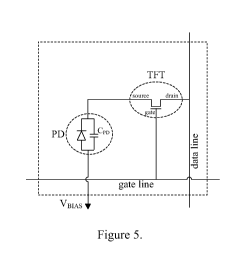
An example of a pixel circuit for an indirect detection, active matrix imaging
array is
schematically illustrated in Figure 5. The circuit elements depicted in this
figure include the
photodiode (PD) and the pixel addressing transitor (TFT). The source, drain
and gate of the
TFT, surrounded by a dashed ellipse, are labelled. A second dashed ellipse
emphasizes that
the photodiode, which is the optical sensor for the pixel, also serves as the
pixel storage
capacitor, with a capacitance of CPD. The gate address line and data address
line
corresponding to the row and column, respectively, of the depicted pixel are
also shown. The
magnitude of the reverse bias voltage applied to the top electrode of the
photodiode is VB!AS.
This voltage is provided by an external voltage supply. VBIAS is typically set
to a value in the
range of -1 V to 8 V.
Figure 6 is a schematic, cross-sectional illustration of one structural
implementation,
referred to as the baseline architecture, of a pixel design corresponding to
the pixel circuit in
Figure 5. In this implementation, the addressing TFT shares the surface area
of the pixel with
a number of other elements including a discrete a-Si photodiode having a
stacked structure,
address lines, and the gaps between the address lines, photodiode and TFT.
In Figure 6, the general location of the a-Si addressing transistor (TFT),
with only the
drain, source and gate illustrated, is indicated by a dashed ellipse. The
bottom electrode of
the photodiode is formed by an extension of the metal used to form the source
of the TFT.
The remaining layers of the photodiode, which do not overlap with the TFT, are
patterned so
as to be aligned with the edges of the bottom electrode and in this way form a
stacked
structure. These layers include a layer of n+ doped a-Si, a layer of intrinsic
a-Si, a layer of p+
doped a-Si, and a layer of ITO serving as an optically transparent top
electrode. A reverse
bias voltage, of magnitude VBIAS, is applied to the top electrode of the
photodiode by way of
11
CA 02765702 2011-12-15
WO 2010/148060 PCT/US2010/038777
a bias line, creating an electric field, k, across the photodiode. The
direction of the data
address line, which is connected to the drain of the TFT by way of a metal
via, and of the bias
line, is orthogonal to the plane of the drawing. The approximate location of
passivation
material is schematically indicated by shading. This includes passivation
material that is
deposited over the entire top surface of the array in order to encapsulate the
array, protecting
the array mechanically and preventing unintended electrical contact with the
bias and data
address lines. An x-ray converter in the form of a scintillator, which extends
over the entire
array, is also depicted. Incident x-rays (wavy arrows) generate optical
photons (straight, faint
arrows) in the scintillator. Some of the optical photons enter the intrinsic
layer of the
photodiode creating electrons and holes which drift toward the electrodes by
virtue of the
electric field, thereby creating imaging signal that is stored in, and
eventually read out from,
the pixel.
For direct detection, active matrix, flat-panel imagers, the converter can
take the form
of a layer of photoconductive material, with a thickness sufficient to stop a
large fraction of
the incident x-rays. One suitable photoconductive material is amorphous
selenium, a-Se,
which can be fabricated up to -2000 pm thick, and is preferably fabricated
with thicknesses
ranging from -200 to 1000 m. Other photoconductive materials that are
suitable as direct
detection converters include single crystal and polycrystalline forms of lead
iodide (Pb12),
mercuric iodide (H912), lead oxide (PbO), cadmium zinc telluride (CdZnTe),
cadmium
telluride (CdTe), Bi2S3, Bi2Se3, BiI31 BiBr3, CdS, CdSe, HgS, Cd2P3, InAs,
InP, In2S3, In2Se3,
-2 -3
Ag2S, Pb14 and Pb2I7 . The choice of thickness for the photoconductor
increases with
increasing x-ray energy, so as to achieve conversion of a reasonably large
fraction of the x-
rays, which can be anywhere from -10% to 90% at diagnostic energies and from -
1 % to 10%
at radiotherapy energies.
12
CA 02765702 2011-12-15
WO 2010/148060 PCT/US2010/038777
In the case of imaging using megavoltage radiation, for example for external
beam
radiation therapy imaging or for industrial radiography, including scanning
for security
applications, a thin (-1 mm) metal plate is typically positioned over the
converter (directly on
the scintillator, for indirect detection, or directly on the encapsulation
over the top electrode
covering the photoconductor for direct detection). The composition of this
plate can take
many forms including copper, steel, tungsten and lead. An example of a pixel
circuit for a
direct detection, active matrix imaging array is schematically illustrated in
Figure 7. The
circuit elements depicted in this figure include the photoconductor (PC), the
pixel addressing
transistor (TFT), and (as indicated by a dashed ellipse) a pixel storage
capacitor with
capacitance CSTORAGE. The source, drain and gate of the TFT, surrounded by
another dashed
ellipse, are labelled. A third dashed ellipse emphasizes that the
photoconductor has
capacitance Cpc and also acts like a large resistor, of resistance Rpc, in the
circuit. The gate
address line and data address line corresponding to the row and column of the
depicted pixel
are also shown. The magnitude of the bias voltage applied to the top electrode
of the
photoconductor is VBIAS. This voltage is provided by an external voltage
supply. The value
of VBIAS used depends upon the type of photoconductor material and generally
increases in
proportion to the layer thickness of that material. For a-Se, VBIAS is
typically -10 V per
micron of thickness. Thus, for a 1000 pm layer of a-Se, VBIAS will be -10,000
V. For HgI2,
VBIAS is typically in the range of -0.5 to 2.0 V per micron. Thus, for a 500
pm layer of HgI2,
VBIAS will be -250 to 1,000 V. The photoconductive layer can also be operated
in avalanche
mode, with the value of VBIAS across that layer typically higher - in the
range of -50 V to 100
V per micron for the example of a-Se. In this case, the avalanche layer may be
made
sufficiently thick to stop a large fraction of x-rays itself, or it may be
made thin, with a layer
of photoconductor or scintillator (such as a-Se or CsI:Tl, respectively, of
sufficient thickness
13
CA 02765702 2011-12-15
WO 2010/148060 PCT/US2010/038777
to stop a large fraction of the incident x-rays) deposited over it. In this
case, the purpose of
the avalanche layer is to amplify the signal from the overlying converter.
Figure 8 is a schematic, cross sectional illustration of one structural
implementation of
a pixel design corresponding to the pixel circuit in Figure 7. In this
implementation, the
addressing TFT shares the surface area of the pixel with the pixel storage
capacitor, with the
address lines, and with gaps between the address lines, storage capacitor and
TFT. The
photoconductor structure (including a bottom electrode, a layer of
photoconductive material,
and a top electrode) resides above the plane (i.e., above the level) of the
addressing TFT.
In Figure 8, the general location of the a-Si addressing transistor (TFT),
with only the
drain, source and gate illustrated, is indicated by a dashed ellipse. For the
pixel storage
capacitor, the location of which is indicated by a second dashed ellipse, only
the top and
bottom electrodes are illustrated. The top electrode of the pixel storage
capacitor is formed
by a back contact, which is an extension of the metal used to form the source
of the TFT.
The bottom electrode for the photoconductor is connected to the TFT by way of
a via
(indicated by a third ellipse) to the back contact, and does not extend over
the TFT. A thick,
continuous layer of photoconductor material (which acts as an x-ray converter)
is deposited
across the entire array, putting that material in contact with the bottom
electrode. A
continuous top electrode is deposited over the entire photoconductor surface.
A bias voltage,
of magnitude VBIAS, is applied to the top electrode so as to establish an
electric field across
the photoconductor. A layer of material, referred to as encapsulation or as an
encapsulation
layer, is deposited over the entire top electrode in order to encapsulate the
array, protecting
the array mechanically and chemically, and preventing unintended electrical
contact with the
top electrode. The direction of the data address line, which is connected to
the drain of the
TFT by way of a metal via, is orthogonal to the plane of the drawing. The
location of
passivation material is approximately indicated by shading. Note that in
alternate
14
CA 02765702 2011-12-15
WO 2010/148060 PCT/US2010/038777
configurations of direct detection pixels and arrays, a thin layer of material
(typically -1 to 10
microns thick, acting as a barrier, dielectric or doped layer) may be
deposited between the
bottom electrode and the photoconductor, or between the top electrode and the
photoconductor. Alternatively, such a thin layer of material may be deposited
in both
locations, and may be different in type and thickness in each location.
For indirect detection active matrix imaging arrays having the baseline
architecture
illustrated in Figure 6, the addressing TFT and the photodiode are in direct
competition with
each other, and with other pixel elements, for area in the pixel. This is
apparent in Figure 6
as well as in a corresponding schematic rendering of four pixels appearing in
Figure 9. It is
further apparent in Figure 10 in which photomicrographs of pixels obtained
from a pair of
indirect detection active matrix arrays are shown. Generally, indirect
detection active matrix
arrays are designed so as to make the area of the photodiode as large as
possible. In addition,
for array designs in which the bias line extends over the top surface of the
photodiode, the
area of these lines and of associated vias (both of which are optically opaque
and block light
from reaching the photodiode) are made as small as possible. For a given array
design, the
fraction of the pixel area that is occupied by photodiode surface that is open
to incident light
from above is referred to as the optical fill factor.
Maximization of optical fill factor is motivated by the fact that more
efficient use of
the incident light from the overlying scintillator increases pixel signal
size, and thus the
signal-to-noise ratio of the imager, leading to improved image quality.
Maximizing optical
fill factor is particularly important for array designs that serve
applications requiring small
pixel pitches (for example, under -100 pm), or applications in which the
imager is operated
at low exposures (such as the low exposure region of fluoroscopy, where the
exposure per
frame is less than -1 MR).
CA 02765702 2011-12-15
WO 2010/148060 PCT/US2010/038777
A high optical fill factor encourages minimization of the size of the
addressing TFT,
the widths of the address lines, the width of the bias line, and the gaps
between the
photodiode, the TFT and the address lines. However, the fabrication process
imposes a
minimum feature size on every element of the design. Furthermore, the address
and bias
lines must be sufficiently wide to limit the electrical resistance along these
lines (since high
resistance would negatively affect the temporal and/or electrical operation of
the array, as
well as possibly decrease signal-to-noise performance). In addition, the gaps
must not be so
narrow as to lead to unintended contact (and thus electrical shorting) between
pixel elements
or to high levels of parasitic capacitance (which can degrade the signal-to-
noise ratio and the
temporal performance). Finally, the ratio of the width to length of the TFT
channel (called
the aspect ratio) must be sufficiently large so as to provide the magnitude of
TFT-on current
required for the desired array readout speed (since TFTs with higher aspect
ratios provide
higher levels of current in their conducting mode). Figure 10 illustrates a
practical example
of these considerations in which the optical fill factor of an early array
design, shown in
Figure 10(a), has been significantly increased in a later design, shown in
Figure 10(b),
through decreases in the sizes of gaps, address lines and the TFT, assisted by
a decrease in
the minimum feature size. The challenge of maintaining a large optical fill
factor becomes
more difficult as pixel pitch decreases, since the area occupied by the
address lines, gaps, and
addressing TFT consumes an ever-greater fraction of the pixel area.
A highly effective method to circumvent the aforementioned restrictions on
optical
fill factor is to implement pixel architectures in which the photodiode
structure is positioned
above the plane (i.e., above the level) of the addressing TFT. A variety of
such out-of-plane
architectures are possible, and two such architectures are shown in Figures 11
and 12. In
these illustrations, the out-of-plane photodiode structure overlaps a portion,
or all, of the
addressing TFT, in order to maximize optical fill factor.
16
CA 02765702 2011-12-15
WO 2010/148060 PCT/US2010/038777
The photodiode in Figure 11 includes a discrete, stacked structure aligned
with the
bottom electrode. As in Figure 6, a single addressing TFT is connected to a
discrete a-Si
photodiode with three a-Si layers and with top and bottom electrodes. However,
in this pixel
architecture, the bottom electrode of the photodiode is located above the
plane of the
addressing TFT. The bottom electrode is connected to the TFT by way of a via
(the location
of which is indicated by a dashed ellipse) to the back contact, which is an
extension of the
metal used to form the source of the TFT. The a-Si layers and the top
electrode of the
photodiode are patterned to form a stack aligned with the bottom electrode.
The direction of
both the data address line (the location of which is indicated by the solid
ellipse), and the bias
line is orthogonal to the plane of the drawing.
The photodiode in Figure 12 has a structure in which some of the layers are
continuous. As in Figure 11, a single addressing TFT is connected to an a-Si
photodiode
located above the plane of the TFT. However, in this pixel architecture, the
p+ doped and
intrinsic layers are not patterned, but rather are continuous across the array
to assist in
maximizing the optical fill factor. The n+ doped a-Si layer is patterned to
align with the
bottom electrode of the photodiode to inhibit charge sharing between
neighboring pixels.
The bottom electrode is connected to the TFT by way of a via (the location of
which is
indicated by a dashed ellipse) to the back contact, which is an extension of
the metal used to
form the source of the TFT. The direction of the data address line (the
location of which is
indicated by the solid ellipse) is orthogonal to the plane of the drawing.
Figures 13 and 14 correspond to an actual realization of an indirect detection
active
matrix array design having the pixel architecture portrayed in Figure 12.
Figure 13 is a
schematic rendering of four pixels while Figure 14 is a photomicrograph of a
pixel from an
array.
17
CA 02765702 2011-12-15
WO 2010/148060 PCT/US2010/038777
SUMMARY OF THE INVENTION
In one embodiment of the present invention, there is provided a radiation
sensor
including a scintillation layer configured to emit photons upon interaction
with ionizing
radiation and a photodetector including in order a first electrode, a
photosensitive layer, and a
photon-transmissive second electrode disposed in proximity to the
scintillation layer. The
photosensitive layer is configured to generate electron-hole pairs upon
interaction with a part
of the photons. The radiation sensor includes pixel circuitry electrically
connected to the first
electrode and configured to measure an imaging signal indicative of the
electron-hole pairs
generated in the photosensitive layer and a planarization layer disposed on
the pixel circuitry
between the first electrode and the pixel circuitry such that the first
electrode is above a plane
including the pixel circuitry. A surface of at least one of the first
electrode and the second
electrode at least partially overlaps the pixel circuitry and has a surface
inflection above
features of the pixel circuitry. The surface inflection has a radius of
curvature greater than
one half micron.
In another embodiment of the present invention, there is provided a radiation
sensor
including a photoconductor detector including in order a first electrode, a
photoconductive
layer, and an ionizing radiation transmissive second electrode. The
photoconductive layer is
configured to generate electron-hole pairs upon interaction with ionizing
radiation. The
radiation sensor includes pixel circuitry electrically connected to the first
electrode and
configured to measure an imaging signal indicative of the electron-hole pairs
generated in the
photoconductive layer and a planarization layer disposed on the pixel
circuitry between the
first electrode and the pixel circuitry such that the first electrode is above
a plane including
the pixel circuitry. A surface of at least one of the first electrode and the
second electrode at
least partially overlaps the pixel circuitry and has a surface inflection
above features of the
pixel circuitry. The surface inflection has a radius of curvature greater than
one half micron.
18
CA 02765702 2011-12-15
WO 2010/148060 PCT/US2010/038777
In yet another embodiment of the present invention, there is provided a method
for
fabricating a radiation sensor. The method includes forming pixel circuitry
elements on a
base substrate, forming a planarization layer over the pixel circuitry
elements, forming a hole
in the planarization layer to expose a connection to the pixel circuitry
elements, metallizing
the patterned hole, forming a first electrode in electrical contact to the
metallized hole, and
forming on the first electrode a layer sensitive to light or ionizing
radiation. Forming the
planarization layer provides, on a surface of the first electrode at least
partially overlapping
the pixel circuitry, a surface inflection, above features of the pixel
circuitry, having a radius
of curvature greater than one half micron.
It is to be understood that both the foregoing general description of the
invention and
the following detailed description are exemplary, but are not restrictive of
the invention.
BRIEF DESCRIPTION OF THE DRAWINGS
A more complete appreciation of the invention and many of the attendant
advantages
thereof will be readily obtained as the same becomes better understood by
reference to the
following detailed description when considered in connection with the
accompanying
drawings, wherein:
Figure 1 is a schematic, three-dimensional drawing of one form of an a-Si thin-
film
transistor (TFT) showing the top of the TFT viewed from an oblique angle;
Figure 2 is a schematic, cross-sectional view of the a-Si TFT shown in Figure
1;
Figure 3 is a schematic, three-dimensional drawing of one form of a poly-Si
TFT
showing the top of the TFT viewed from an oblique angle;
Figure 4 is a schematic, cross-sectional view of the poly-Si TFT shown in
Figure 3;
Figure 5 is a schematic circuit diagram for a pixel from an active matrix
imaging
array employing indirect detection of the incident radiation;
19
CA 02765702 2011-12-15
WO 2010/148060 PCT/US2010/038777
Figure 6 is a schematic drawing of a cross sectional view of one form of an
indirect
detection pixel design having a discrete photodiode, corresponding to one
particular structural
implementation of the pixel circuit of Figure 5 and referred to as the
baseline architecture;
Figure 7 is a schematic circuit diagram for a pixel from an active matrix
imaging
array employing direct detection of the incident radiation;
Figure 8 is a schematic drawing of a cross sectional view of one form of a
direct
detection pixel design;
Figure 9 is a schematic rendering of four adjacent pixels of an indirect
detection
active matrix array, corresponding to an implementation of the pixel circuit
and baseline
architecture shown in Figures 5 and 6, respectively;
Figure 10 is a collection of photomicrographs of the top surface of a pair of
indirect
detection active matrix arrays in the region of a single pixel, corresponding
to an
implementation of the baseline architecture in Figure 6;
Figure 11 is a schematic drawing of a cross sectional view of an indirect
detection
pixel design with a discrete, out-of-plane, photodiode structure;
Figure 12 is a schematic drawing of a cross sectional view of an indirect
detection
pixel design with a continuous, out-of-plane, photodiode structure;
Figure 13 is a schematic rendering of four adjacent pixels of an indirect
detection
active matrix array, corresponding to an implementation of the pixel circuit
and architecture
shown in Figures 5 and 12, respectively;
Figure 14 is a photomicrograph of the top surface of an indirect detection
active
matrix array in the region of a single pixel, corresponding to an
implementation of the pixel
architecture in Figure 12 and to the rendering in Figure 13;
Figure 15 is a schematic circuit diagram for a pixel from an indirect
detection array
based on an active pixel design with a one-stage, in-pixel amplifier;
CA 02765702 2011-12-15
WO 2010/148060 PCT/US2010/038777
Figure 16 is a schematic rendering of four adjacent pixels of an indirect
detection
array based on an active pixel design employing poly-Si TFTs, corresponding to
an
implementation of the pixel circuit in Figure 15 and a photodiode structure
similar to that in
Figure 12;
Figure 17 is a photomicrograph of the top surface of an indirect detection
array in the
region of a single pixel, corresponding to an implementation of the pixel
circuit in Figure 15
and to the rendering in Figure 16;
Figure 18 is a schematic circuit diagram for a pixel from an indirect
detection array
based on an active pixel design with a two-stage, in-pixel amplifier;
Figure 19 is a schematic rendering of four adjacent pixels of an indirect
detection
array based on an active pixel design employing poly-Si TFTs, corresponding to
an
implementation of the pixel circuit in Figure 18 and a photodiode structure
similar to that in
Figure 12;
Figure 20 is a photomicrograph of the top surface of an indirect detection
array in the
region of a single pixel, corresponding to an implementation of the pixel
circuit in Figure 18
and to the rendering in Figure 19;
Figure 21 is a calculated cross sectional view of an indirect detection array
based on a
one-stage, in-pixel amplifier design employing poly-Si TFTs, corresponding to
Figures 16
and 17 and showing the native topology of various features and materials;
Figure 22(a) is a calculated cross sectional view of an indirect detection
array based
on a two-stage, in-pixel amplifier design employing poly-Si TFTs,
corresponding to Figures
19 and 20 and showing the native topology of various features and materials;
Figure 22(b) corresponds to a portion of Figure 22(a);
21
CA 02765702 2011-12-15
WO 2010/148060 PCT/US2010/038777
Figure 23(a), obtained from the same calculations used for Figure 21, is a top
view of
a one-stage, in-pixel amplifier array in the region of a single pixel,
corresponding to Figures
16 and 17 and showing the native topology of the top of the continuous
photodiode structure;
Figure 23(b) is a photomicrograph, obtained from Figure 17, shown for purposes
of
comparison with the calculated top view in Figure 23(a);
Figure 24(a), obtained from the same calculations used for Figure 22, is a top
view of
a two-stage, in-pixel amplifier array in the region of a single pixel,
corresponding to Figures
19 and 20, and showing the native topology of the top of the continuous
photodiode structure;
Figure 24(b) is a photomicrograph, obtained from Figure 20, shown for purposes
of
comparison with the calculated top view in Figure 24(a);
Figure 25 is a pair of drawings illustrating the general concept of radius of
curvature,
which can be applied to the characterization of changes in the planarity of a
surface;
Figure 26(a) is a calculated cross sectional view of an indirect detection
array,
corresponding to Figure 21, but with a more uniform topology achieved through
complete
planarization of passivation #2;
Figure 26(b) is a calculated cross sectional view of an indirect detection
array,
corresponding to Figure 21, but with a more uniform topology achieved through
partial
planarization of passivation #2;
Figure 27(a) is a calculated cross sectional view of an indirect detection
array,
corresponding to Figure 22(a), but with a more uniform topology achieved
through complete
planarization of passivation #2;
Figure 27(b) corresponds to a portion of Figure 27(a);
Figure 28 is a calculated cross sectional view of an indirect detection array,
corresponding to Figure 26(a), but with a more uniform topology achieved
through
smoothing of the peripheral edges of the bottom electrode of the photodiode;
22
CA 02765702 2011-12-15
WO 2010/148060 PCT/US2010/038777
Figure 29 is a calculated cross sectional view of an indirect detection array,
corresponding to Figure 27(a), but with a more uniform topology achieved
through
smoothing of the peripheral edges of the bottom electrode of the photodiode;
Figure 30 is a calculated cross sectional view of an indirect detection array,
corresponding to Figure 28, but with a more uniform topology achieved through
narrowing of
the vias that connect the bottom electrode of the photodiode with the back
contact and filling
those vias with metal;
Figure 31(a), obtained from calculations and corresponding exactly to Figure
23(a), is
a top view of a one-stage, in-pixel amplifier array in the region of a single
pixel, showing the
native topology of the top continuous photodiode structure, and included for
purposes of
comparisons with the remaining views in this figure;
Figure 31(b), obtained from the same calculations used for Figure 26(a), shows
the
improvement in surface topology, relative to Figure 31(a), achieved through
complete
planarization of passivation #2;
Figure 31(c), obtained from the same calculations used for Figure 28, shows
the
improvement in surface topology, relative to Figure 31(b), achieved through
smoothing of the
peripheral edges of the bottom electrode of the photodiode;
Figure 31(d), obtained from the same calculations used for Figure 30, shows
the
improvement in surface topology, relative to Figure 31(c), achieved through
narrowing of the
vias that connect the bottom electrode of the photodiode with the back contact
and filling
those vias with metal;
Figure 32(a), obtained from calculations and corresponding exactly to Figure
24(a), is
a top view of a two-stage, in-pixel amplifier array in the region of a single
pixel, showing the
native topology of the top continuous photodiode structure, and included for
purposes of
comparisons with the remaining views in this figure;
23
CA 02765702 2011-12-15
WO 2010/148060 PCT/US2010/038777
Figure 32(b), obtained from the same calculations used for Figure 27, shows
the
improvement in surface topology, relative to Figure 32(a), achieved through
complete
planarization of passivation #2;
Figure 32(c), obtained from the same calculations used for Figure 29, shows
the
improvement in surface topology, relative to Figure 32(b), achieved through
smoothing of the
peripheral edges of the bottom electrode of the photodiode;
Figure 32(d), obtained from calculations, shows the improvement in surface
topology,
relative to Figure 32(c), achieved through narrowing of the vias that connect
the bottom
electrode of the photodiode with the back contact and filling those vias with
metal;
Figure 33(a) is a calculated cross sectional view of an indirect detection
array,
corresponding to Figure 21, but with a more uniform topology achieved through
complete
planarization of the layer of intrinsic a-Si in the photodiode;
Figure 33(b) is a calculated cross sectional view of an indirect detection
array,
corresponding to Figure 21, but with a more uniform topology achieved through
partial
planarization of the layer of intrinsic a-Si in the photodiode;
Figure 34(a), obtained from calculations and corresponding exactly to Figure
23(a), is
a top view of a one-stage, in-pixel amplifier array in the region of a single
pixel, showing the
native topology of the top continuous photodiode structure, and included for
purposes of
comparisons with the remaining views in this figure;
Figure 34(b), obtained from the same calculations used for Figure 33(b), shows
improvement in surface topology, relative to 34(a), achieved through partial
planarization of
the layer of intrinsic a-Si in the photodiode;
Figure 34(c), obtained from the same calculations used for Figure 33(a), shows
improvement in surface topology, relative to 34(a), achieved through complete
planarization
of the layer of intrinsic a-Si in the photodiode;
24
CA 02765702 2011-12-15
WO 2010/148060 PCT/US2010/038777
DETAILED DESCRIPTION OF THE EMBODIMENTS
The incorporation of out-of-plane photodiode structures into the pixel design
of
indirect detection active matrix arrays provides a mechanism for significantly
improving
optical fill factor. In the case of the implementation of continuous
photodiode structures,
optical fill factors as large as unity, corresponding to the entire area of
the pixel, are possible.
Such optical fill factor improvements result from eliminating the competition
for pixel area
between the photodiode and other pixel elements such as the addressing TFT,
address lines
and gaps.
Out-of-plane photodiode structures also make it possible to introduce
additional
elements to the pixels (such as TFI's, diodes, capacitors and resistors, as
well as vias, traces,
control lines, address lines and ground planes), thereby making more complex
pixel circuits
possible. As in the case of active matrix arrays, these additional elements
would reside in a
separate plane from that of the photodiode and therefore would not compete
with the
photodiode for pixel area. Through introduction of more complex circuits, both
in the pixel
design and elsewhere in the array design, considerable improvements in
performance can be
achieved compared to that of active matrix flat panel imaging arrays in which
each pixel has
only a single TFT (acting as the pixel addressing switch). While the type of
semiconductor
material used for these additional TFTs and diodes can be any of those
described above, the
examples of more complex circuits described below involve poly-Si TFTs. In
addition, while
the following examples pertain to indirect detection array designs in which
the imaging signal
is collected and stored in a pixel storage capacitor prior to readout, out-of-
plane photodiode
structures also make it possible to create pixel circuits that allow the
detection and counting
of individual x-rays, a capability commonly referred to as single photon
counting, without
these circuits competing for area with the photodiode. Such single photon
counting pixels
CA 02765702 2011-12-15
WO 2010/148060 PCT/US2010/038777
would include a detector (such as an out-of-plane photodiode structure) as
well as circuits for
an amplifier, a discriminator (optionally with a pulse-shaping circuit), and
an event counter
(e.g., in the form of a linear feed-back shift register), as well as for
addressing and pixel reset.
Single photon counting arrays offer many advantages such as the ability to
create high
contrast images based on a selected portion of the x-ray spectrum, a technique
referred to as
energy discrimination or energy windowing.
Increased complexity can improve the signal-to-noise ratio of the imager, both
for
array designs based on indirect detection as well as direct detection of the
incident radiation.
In the case of indirect detection, greater complexity can also help to limit
undesirable effects
associated with trapping and release of charge in the metastable electronic
states (also called
the trapping states) of the a-Si in the photodiodes.
Referring now to the drawings, wherein like reference numerals designate
identical or
corresponding parts throughout the several views and, more particularly, to
Figure 5, for
active matrix array pixel circuits having the general form shown in Figure 5,
during readout
of a given row of pixels, the electric field across the corresponding
photodiodes increases
back to the maximum value defined by the magnitude of VBIAS and by the
thickness of the a-
Si in the photodiode. Thus, pixel readout results in the imaging signals being
sampled as well
as the pixels being initialized. During collection of imaging signal in each
pixel storage
capacitor, the electric field decreases. For a given pixel, if the imaging
signal is sufficiently
large, the magnitude of the electric field will decrease almost to zero, the
storage capacitor
will be able to store no further charge, and the pixel is saturated. The
probability of charge
trapping in the photodiode typically increases with decreasing electric field
strength, and
becomes very high near conditions of pixel saturation. In radiographic imaging
(which
typically involves large x-ray exposures), high levels of trapped charge
result in substantial
loss of imaging signal. This reduces the signal-to-noise ratio for the imager
and can degrade
26
CA 02765702 2011-12-15
WO 2010/148060 PCT/US2010/038777
image quality. In fluoroscopic imaging, charge trapped during acquisition of
early images
will be released in later images. This can result in image information from
earlier images
appearing in later images - a generally undesirable effect which is referred
to as lag or image
lag. In addition, if an imager is used to generate a radiographic image with a
large x-ray
exposure, and if that imager is used to generate fluoroscopic images a short
time later, image
information from the radiographic image may appear in the fluoroscopic images -
an
undesirable effect which is referred to as ghosting. Lag and ghosting are
responsible for
image artifacts that can obscure important information in an image, thus
degrading the
usefulness of the image, and such artifacts are commonly encountered with
imagers based on
active matrix arrays. However, array designs incorporating circuits of greater
complexity
than those of active matrix arrays can overcome signal-to-noise limitations
and reduce image
artifacts, while preserving the important advantages of compactness, large
area, and radiation
damage resistance.
An example of a more complex pixel circuit for an indirect detection array is
schematically illustrated in Figure 15. This circuit design includes three
TFTs that are
configured to provide a one-stage, in-pixel amplifier, an addressing TFT and a
reset TFT. By
virtue of the presence of the in-pixel amplifier, this design is referred to
as an active pixel
design. During operation of an array incorporating this design, imaging signal
is collected
and stored in the photodiode, which acts as the pixel storage capacitor. As in
the case of
active matrix arrays, readout can be performed one row of pixels at a time (if
maximum
spatial resolution is desired), but sampling of the pixel signals and pixel
initialization are no
longer concurrent. When the imaging signal in a given pixel storage capacitor
is sampled
through use of the addressing TFT, the in-pixel amplifier magnifies the signal
by an amount
equal to the ratio of the capacitance of the data address line to the
capacitance of the
photodiode, CPD. Since this amplification occurs at a point in the imager
circuit prior to
27
CA 02765702 2011-12-15
WO 2010/148060 PCT/US2010/038777
contributions of noise from the addressing TFT and from the external
preamplifier (which are
two of the major noise sources in active matrix imagers), this pixel circuit
design can provide
a substantial increase in the signal-to-noise ratio of the imager. In
addition, for this pixel
circuit, sampling the imaging signal does not initialize the pixel. Rather,
the imaging signal
continues to reside in the pixel storage capacitor until the pixel is
initialized through use of
the reset TFT. As a consequence, the imaging signals can be sampled multiple
times and
then averaged, leading to further improvement in the signal-to-noise ratio of
the imager.
Figures 16 and 17 correspond to an actual realization of an indirect detection
array with a
one-stage, in-pixel amplifier design, representing an implementation of the
pixel circuit of
Figure 15. Figure 16 is a schematic rendering of four pixels, while Figure 17
is a
photomicrograph of a pixel from an actual array.
Another example of an even more complex pixel circuit for an indirect
detection array
is schematically illustrated in Figure 18. This circuit design includes five
TFTs and a feed-
back capacitor that are configured to provide a two-stage, in-pixel amplifier,
an addressing
TFT and a reset TFT. This is another example of an active pixel design. During
operation of
an array incorporating this design, imaging signal is collected and stored in
the feed-back
capacitor, which acts as the pixel storage capacitor. The operation and
advantages of this
design are similar to that of the one-stage, in-pixel amplifier design
described above -
providing a substantial increase in the signal-to-noise ratio of the imager by
virtue of in-pixel
amplification of the imaging signal, as well as by virtue of multiple sampling
and averaging
of the imaging signal. In addition, during collection and storage of the
imaging signal, the
electric field across the photodiode decreases only very slightly in this
design - in marked
contrast to the situation for an active matrix pixel design or the previously
described one-
stage in-pixel amplifier design.
28
CA 02765702 2011-12-15
WO 2010/148060 PCT/US2010/038777
Consequently, the amount of charge trapping in the photodiode is reduced and
lag and
ghosting artifacts are lessened, even at very high x-ray exposures. A further
advantage of this
two-stage in-pixel amplifier design is that it allows a greater measure of
control over the gain
of the amplifier (defined as the multiplicative factor by which the amplifier
increases the
imaging signal) compared to that of the one-stage design. In the two-stage
design, the in-
pixel amplifier magnifies the imaging signal by an amount equal to the ratio
of the
capacitance of the data address line to the capacitance of the pixel feed-back
capacitor, CFB.
Thus, for a given pixel pitch and pixel storage capacitor capacitance, the
magnitude of the in-
pixel amplifier gain increases with increasing data line capacitance, both for
the one-stage
and two-stage design. As a consequence, if larger arrays (i.e., arrays with
greater numbers of
pixels along the data line direction) are manufactured based on a given pixel
design, the
amount of amplification will increase. This is a result of the fact that data
line capacitance
will increase in proportion to the number of pixels along a data address line.
In the case of
the one-stage design, this dependence (which is generally undesirable) of in-
pixel amplifier
gain on array size cannot be offset without altering the thickness or area of
the photodiode
(whose specifications need to be independently optimized for maximum light
detection
efficiency). However, for the two-stage design, the magnitude of CFB can be
adjusted (for
example, by adjusting the thickness of the capacitor dielectric or area of the
capacitor) to
offset changes in data line capacitance. This allows a given two-stage design
to be
implemented for various array sizes without changing the range of the
magnitude of imaging
signals extracted from the array - thus simplifying the design of the external
preamplification
electronics required for imager operation. Figures 19 and 20 correspond to an
actual
realization of an indirect detection array with a two-stage, in-pixel
amplifier, representing an
implementation of the pixel circuit of Figure 18. Figure 19 is a schematic
rendering of four
pixels while Figure 20 is a photomicrograph of a pixel from an actual array.
29
CA 02765702 2011-12-15
WO 2010/148060 PCT/US2010/038777
As described above, out-of-plane photodiode structures make substantial
performance
improvements possible. These improvements are a direct result of increased
optical fill
factor, as well as a result of increased pixel circuit complexity facilitated
by such photodiode
structures. For the practical realization of these benefits, however, the out-
of-plane
photodiode structures should not introduce other factors that degrade
performance. In this
regard, the inventor has discovered a significant problem that degrades
performance, as
explained below.
Figures 21 and 22 are calculated cross sectional views of the one-stage and
two-stage
in-pixel amplifier designs corresponding to the microphotographs in Figures 17
and 20,
respectively. These cross sectional views illustrate various features and
materials present in
the pixel designs. For example, there are four passivation layers: a buffer
passivation,
passivation #1, passivation #2 and a top passivation. In addition, there are
four metal layers:
shunt metal (used for such elements as the reset voltage lines and the gate
address lines);
metal #1 (used for such elements as the back contacts, data address lines and
vias); metal #2
(used for such elements as the bottom electrode of the photodiode); and ITO
(used for the top
electrode of the photodiode). Other layers and features shown in Figures 21
and 22 include:
the poly-Si used for the TFT channels (labeled as active poly-Si); TFT gates
(formed from
poly-Si); and n+ doped, intrinsic and p+ doped a-Si used for the photodiode.
The topological
non-uniformity of the photodiode structures that is apparent in these cross
sections is
representative of that in the corresponding fabricated arrays, from which the
photomicrographs in Figures 17 and 20 were obtained. For example, in Figures
23 and 24,
the close correspondence between top views of the pixels (obtained from the
same
calculations used to generate the cross sectional views in Figures 21 and 22),
and
photomicrographs of actual realizations of the corresponding arrays, is
apparent.
CA 02765702 2011-12-15
WO 2010/148060 PCT/US2010/038777
The photodiode structures illustrated in Figures 21 to 24 demonstrate a very
high
degree of non-uniformity in their topology. This topological non-uniformity
results from the
presence of features in the pixel design which are located below, or are part
of, the
photodiode. For the examples of the pixel design shown, these features include
TFTs,
capacitors, address lines, traces and vial, including the vias that connect
the bottom electrode
of the photodiode to the back contact. Such features create non-uniformity in
an out-of-plane
photodiode structure whether the structure is continuous (as in these
examples) or discrete
(i.e., having the photodiode structure shown in Figure 11). Note that, in the
case of a direct
detection array, the presence of features (such as TFTs, capacitors, address
lines, traces and
vias) that are below, or are part of, the photoconductor structure creates a
similar degree of
topological non-uniformity in that structure as well. For an indirect
detection array with a
continuous out-of-plane photodiode structure, as well as for a direct
detection array, a
topological non-uniformity is created along the entire perimeter of the bottom
electrode and
in the region of the via connecting the bottom electrode to the back contact,
as is apparent in
Figures 14, 21 and 22(a).
By comparison, for indirect detection arrays employing the baseline
architecture, the
discrete photodiode structures demonstrate a very high degree of uniformity in
their topology.
This topological uniformity results from the absence of any features in the
pixel design which
are located below, or are part of, the photodiode, as is apparent in Figures 6
and 9. In this
case, when the processing steps used to fabricate the various layers of the
photodiode
structure are performed over the smooth, flat surface of the array substrate,
a smooth and
planar surface, as well as a uniformity of thickness, is achieved for each
layer. Consequently,
the top of the photodiode structure will be smooth and planar, as observed in
Figure 10. This
smoothness and planarity is limited only by random, local variations (on the
order of several
hundred angstroms) that originate from processing steps used in the
fabrication of arrays.
31
CA 02765702 2011-12-15
WO 2010/148060 PCT/US2010/038777
Note that, during fabrication, other processing variations can create a
systematic variation
(e.g., an increase or a decrease) in the thickness of a given layer of
material of up to several
tens of percent across an array.
In the case of indirect detection arrays employing the baseline architecture,
the
photodiodes exhibit excellent properties, including high efficiency for the
sensing of optical
photons and the collection of the resulting signal, and favorably low levels
of dark current,
charge trapping, charge release and lag - with neither random local variations
in smoothness
and planarity nor systematic variations in material thickness due to the
fabrication process
interfering with these excellent properties. Photodiode structures that
exhibit such excellent
properties, whether comprising a discrete, baseline architecture design, or a
continuous or
discrete out-of-plane design, are referred to as being of high quality. For a
given imaging
array, each of these properties can be obtained through measurements of the
signal properties
of individual pixels and the results from an individual pixel, or from the
average of results
from many pixels, can be expressed in the following manner. The magnitude of
this
favorable level of dark current per pixel, normalized to unit photodiode area,
is less than -1
pA per square mm. The magnitude of this favorable level of charge trapping per
pixel,
quantified by the amount of imaging signal lost to trapping during a single
radiographic
frame, and expressed as a percentage of the imaging signal obtained under
conditions where
charge trapping and charge release are in equilibrium, is less than -20%. The
magnitude of
this favorable level of charge release per pixel, quantified by the amount of
imaging signal
released from trapping states during the first frame acquired in the absence
of radiation
following a series of frames acquired with radiation and under conditions
where charge
trapping and charge release are in equilibrium, and expressed as a percentage
of the imaging
signal obtained under conditions where charge trapping and release are in
equilibrium, is less
than -15%. The magnitude of this favorable level of lag per pixel, quantified
by the amount
32
CA 02765702 2011-12-15
WO 2010/148060 PCT/US2010/038777
of imaging signal (that originates from charge trapped in one or more previous
frames)
released from trapping states during the first frame acquired in the absence
of radiation
following one, or a series of frames acquired with radiation, and expressed as
a percentage of
the imaging signal from the previous frame, is less than -15%. The results of
such
measurements are also commonly referred to as first field lag or,
alternatively, as first frame
lag. For direct detection active matrix arrays employing a photoconductive
material for the
converter, the magnitude of the favorable level of dark current, normalized to
unit
photoconductor area, charge trapping, charge release and lag is similar to the
levels described
above for indirect detection arrays.
For high quality photodiode structures in indirect detection arrays employing
the
baseline architecture, one factor contributing to the excellent properties
described above is
the degree of uniformity in topology. Within the limits of surface smoothness,
surface
planarity, and uniformity of thickness previously described, each of the
individual n+ doped,
intrinsic and p+ doped a-Si layers in the photodiode has a uniform thickness,
the top and
bottom electrodes are both planar, and these electrodes are parallel to each
other. As a
consequence, the manner in which the electric field strength varies as a
function of distance
across the thickness of the intrinsic layer remains relatively unchanged
across the area of the
photodiode, and this is responsible for the favorable levels of dark current,
charge trapping,
charge release and lag in a high quality photodiode.
Conversely, in photodiode structures that have a non-uniform topology, regions
of
very high and very low electric field strength are created in the a-Si
material of the
photodiode. In regions of a photodiode where either a top or bottom electrode
exhibits a
sharp (i.e., abrupt) departure from planarity, the electric field in the
intrinsic a-Si will be
significantly larger than the electric field in regions where the top and
bottom electrodes are
parallel. In the vicinity of such regions of high electric field, the electric
field strength will be
33
CA 02765702 2011-12-15
WO 2010/148060 PCT/US2010/038777
significantly lower than the electric field in regions where the top and
bottom electrodes are
parallel. The sharper (i.e., more abrupt) the change in planarity, the larger
the deviations in
electric field strength will be. Since dark current increases as a function of
increasing electric
field strength, regions of significantly increased electric field strength
will result in
unfavorable levels of dark current. Similarly, since charge trapping increases
as a function of
decreasing electric field strength, regions of significantly reduced electric
field strength will
result in unfavorable levels of charge trapping, charge release and lag.
For the three examples of pixel design with a continuous out-of-plane
photodiode
structure described above (i.e., with an active matrix design, Figure 14, with
a one-stage in-
pixel amplifier design, Figures 21 and 23, and with a two-stage in-pixel
amplifier design,
Figures 22 and 24), the extensive topological non-uniformity of the photodiode
in each
design results in extensive regions of significantly increased electric field
strength, as well as
extensive regions of significantly decreased electric field strength. Sharp
changes in
electrode planarity can also substantially decrease the minimum distance
between the top and
bottom electrode, as is apparent in the region of the deep via in Figure 21,
further
contributing toward significant increases in electric field strength. The
presence of such
regions as the inventor has discovered leads to unfavorably high levels of
dark current,
charge trapping, charge release and lag and thus prevents the realization of
high quality
photodiodes.
High photodiode dark current is undesirable for several reasons. Since dark
signal
(created by dark current) is stored in the pixel storage capacitor during
imaging, high dark
current significantly reduces the range of exposure over which the pixel can
operate before
saturating. In addition, since dark current creates a source of noise referred
to as shot noise,
high dark current leads to high shot noise. Since this contribution of shot
noise in the imager
occurs prior to the effect of gain from an in-pixel amplifier (such as in the
pixel circuit
34
CA 02765702 2011-12-15
WO 2010/148060 PCT/US2010/038777
designs of Figures 15 and 18), the improvement in the signal-to-noise ratio of
the imager is
reduced compared to expectations. Similarly, high shot noise reduces the
intended
improvement in the signal-to-noise ratio of an imager incorporating an AMFPI
array with an
out-of-plane photodiode structure (such as in the pixel designs illustrated in
Figures 11 and
12). High levels of charge trapping are undesirable for several reasons. In
radiographic
imaging, loss of signal to trapping states reduces the imaging signal sampled
from the pixel,
thereby reducing the signal-to-noise ratio of the imager. In addition, high
levels of charge
trapping lead to high levels of charge release and lag, increasing the
undesirable
consequences of image artifacts.
The sharpness (i.e., abruptness) of changes in the planarity of a surface
(such as the
topology of the electrodes in a photodiode as shown in Figures 21 to 24) can
be quantified by
the radius of curvature, r, as illustrated in Figure 25. Sharper changes in
planarity are
therefore represented by smaller values of r. Calculational determinations of
the effect of
sharp changes in electrode planarity (as parameterized by r) on electric field
strength in the
intrinsic a-Si layer of photodiode structures representative of those in
continuous and discrete
out-of-plane designs indicates the importance of reducing such sharp changes
in the
photodiode structure.
In regions near changes of planarity characterized by a value for r of 0.1 m
or less,
the maximum deviations in electric field can be very large, more than 300
percent higher (in
those regions nearest to the change in planarity) and more than 60 percent
lower (in the
vicinity of those regions) than the magnitude of the electric field for a pair
of parallel
electrodes. In regions near changes of planarity characterized by a value for
r of -0.5 m,
deviations in electric field can be up to -300 percent higher (in those
regions nearest to the
change in planarity) and up to -60 percent lower (in the vicinity of those
regions) than the
magnitude of the electric field for a pair of parallel electrodes.
CA 02765702 2011-12-15
WO 2010/148060 PCT/US2010/038777
In regions near changes of planarity characterized by a value for r of - 1 pm,
deviations in electric field can be up to -200 percent higher (in those
regions nearest to the
change in planarity) and up to -50 percent lower (in the vicinity of those
regions) than the
magnitude of the electric field for a pair of parallel electrodes. In regions
near changes of
planarity characterized by a value for r of -2 pm, deviations in electric
field can be up to -50
percent higher (in those regions nearest to the change in planarity) and up to
-30 percent
lower (in the vicinity of those regions) than the magnitude of the electric
field for a pair of
parallel electrodes. In regions near changes of planarity characterized by a
value for r of -5
pm, deviations in electric field can be up to -20 percent higher (in those
regions nearest to
the change in planarity) and up to -15 percent lower (in the vicinity of those
regions) than the
magnitude of the electric field for a pair of parallel electrodes. In regions
near changes of
planarity characterized by a value for r of -10 pm, deviations in electric
field can be to up
-10 percent higher (in those regions nearest to the change in planarity) and
up to -10 percent
lower (in the vicinity of those regions) than the magnitude of the electric
field for a pair of
parallel electrodes.
The above considerations make it clear that, if out-of-plane photodiode
structures are
fabricated without regard to the topological uniformity of the photodiode, the
resulting
topology (which will be referred to as the native topology, such as appears in
the examples
shown in Figures 21 to 24) can prevent realization of high quality photodiodes
and degrade
the performance of imagers that incorporate arrays with such photodiodes. In
general, the
magnitudes of dark current, charge trapping, charge release and lag will
increase as the extent
(i.e., the number and area) of regions with sharp changes in the planarity of
the electrodes of
the photodiodes increases. These magnitudes will also increase as the
sharpness of the
changes in the planarity of the electrodes increases. However, high quality
out-of-plane
photodiode structures are realized according to one embodiment of the
invention where the
36
CA 02765702 2011-12-15
WO 2010/148060 PCT/US2010/038777
photodiodes are designed and fabricated so that the extent of such regions, as
well as the
sharpness of changes in planarity of the electrodes, are sufficiently reduced
so that the
photodiodes exhibit favorable levels of dark current, charge trapping, charge
release and lag.
Figures 26 to 34 show examples of the result of applying various methods to
improve
the topological uniformity of out-of-plane photodiode structures. One method
for improving
topological uniformity is to completely planarize a layer of material that is
below the
photodiode structure. Illustrations of the application of this method appear
in Figures 26(a)
and 31(b) for the case of the one-stage in-pixel amplifier design, and in
Figures 27 and 32(b)
for the case of the two-stage in-pixel amplifier design. In each case, the top
surface of
passivation #2 has been made planar.
This can be achieved, for example in one embodiment of the invention, through
the
application of chemical-mechanical polishing (CMP, also called chemical-
mechanical
planarization) and/or spin coating. In applying this method, the thickness of
the passivation
layer could initially be made thicker than in the native topology case, so as
to ensure a
minimum thickness following the application of CMP. This would help to ensure
that the
parasitic capacitance between the photodiode electrodes and circuit elements
below the
photodiode structure is kept below a desired limit. Figures 26(a) and 27
provide cross
sectional views of the resulting improvement in topological uniformity of the
photodiode
compared to that in the case of the native topologies illustrated in Figures
21 and 22,
respectively. Figures 31(b) and 32(b) provide top views of the resulting
improvement in
topological uniformity of the photodiode compared to the native topology
illustrated in
Figures 31(a) and 32(a), respectively. The effectiveness of this method in
significantly
improving topological uniformity is apparent. Another method for improving
topological
uniformity of out-of-plane photodiode structures is to partially planarize a
layer of material
37
CA 02765702 2011-12-15
WO 2010/148060 PCT/US2010/038777
that is below the photodiode structure, as illustrated in Figure 26(b). This
can be achieved
through use of various known techniques, such as those described above.
In continuous out-of-plane photodiode structures, the edges of the bottom
electrode
(formed from the metal #2 layer) create sharp changes in planarity in the top
electrode, as is
apparent in Figures 26(a) and 27(a). In one embodiment of the invention, it is
desirable to
smooth these edges. One method according to the invention to achieve this
smoothing is
through adjustment of the etching technique used to define the edges of the
bottom electrode
so as to achieve a beveled or rounded shape having a larger radius of
curvature than that in
the native topology. Figures 28 and 29 provide cross sectional views of the
resulting
improvement in topological uniformity of the photodiode compared to that shown
in Figures
26(a) and 27(a), respectively. Figures 31(c) and 32(c) provide top views of
the resulting
improvement in topological uniformity of the photodiode compared to that shown
in Figures
31(b) and 32(b), respectively. The effectiveness of this method in further
improving
topological uniformity is apparent.
In continuous out-of-plane photodiode structures, the one or more vias
connecting the
bottom electrode of the photodiode to the back contact also create sharp
changes in the
planarity of the top and bottom electrodes. One method according to the
invention for
reducing the sharpness of these changes in planarity is to reduce the area of
each via by
narrowing its lateral dimensions (i.e., the dimensions along the surface of
the photodiode), for
example, to the limits allowed by the design rules. The metal used for the
bottom electrode
can also be deposited so as to fill the via. Figure 30 is a cross sectional
view of the resulting
improvement in topological uniformity of the photodiode compared to that shown
in Figure
28. (No corresponding cross-sectional illustration is shown for the two-stage
in-pixel
amplifier design given the absence of vias within the field of view of Figure
29.) Figures
31(d) and 32(d) are top views of the resulting improvement in topological
uniformity of the
38
CA 02765702 2011-12-15
WO 2010/148060 PCT/US2010/038777
photodiode compared to that shown in Figures 31(c) and 32(c), respectively.
The
effectiveness of this method of the invention in further improving topological
uniformity is
apparent.
Another method for improving the topological uniformity of out-of-plane
photodiode
structures is to planarize the top surface of the layer of intrinsic a-Si in
the photodiode.
Illustrations of the application of this method appear in Figures 33, 34(b)
and 34(c) for the
case of the one-stage in-pixel amplifier design.
Complete planarization of the layer of intrinsic a-Si in the photodiode can be
achieved, for example in one embodiment of the invention, through application
of CMP. In
applying this method, the thickness of the intrinsic a-Si layer can initially
be made thicker
than the preferred thickness, so as to ensure that the final thickness
achieved after application
of CMP corresponds to that preferred thickness. This would help to ensure that
the
photodiode exhibits excellent properties. Figure 33(a) provides a cross
sectional view of the
resulting improvement compared to the case of the native topology illustrated
in Figure 21.
Figure 34(c) provides a top view of the resulting improvement in topological
uniformity of
the photodiode compared to the native topology illustrated in Figure 34(a).
The effectiveness
of this method in significantly improving the uniformity of the top electrode
of the
photodiode is apparent. The uniformity of the bottom electrode remains
unchanged
compared to the native topology. Another embodiment of this method for
improving
topological uniformity of out-of-plane photodiode structures is to partially
planarize the layer
of intrinsic a-Si in the photodiode, as illustrated in Figures 33(b) and
34(b). This can be
achieved through the use of various known techniques, such as those described
above.
Methods for improving the topological uniformity of out-of-plane photodiode
structures, as described herein, including planarization of one or more layers
of material
below the photodiode structure, such as a passivation layer, smoothing the
edges of the
39
CA 02765702 2011-12-15
WO 2010/148060 PCT/US2010/038777
bottom electrode of the photodiode structure, narrowing the lateral dimensions
of vias
connecting the bottom electrode of the photodiode to the back contact and/or
depositing the
metal used for the bottom electrode so as to fill the vias, and planarization
of the intrinsic a-Si
in the photodiode, can be used in combination to achieve the desired results
of this invention.
As is clear from the dramatic results shown in Figures 31, 32, and 34, the
invention
provides a capability to remove topological non-uniformities associated with
edges of pixel
circuitry elements. The planarization techniques (as described above)
planarize layers
covering pixel circuitry elements or array features such as the TFTs
(including the source,
drain and gate of TFTs), diodes, capacitors and resistors, as well as vias,
traces, control lines,
address lines, ground planes, electrode surfaces, light blocking surfaces,
bias lines, back
contacts and bottom electrodes of the photodiode (all of which are fabricated
from multiple
metal, passivation, or dielectric layers), discussed above and such as shown
in the sectional
views of Figures 26-30 and 33. In this manner, the invention is not limited to
planarization
over thin film transistor elements. For example, even the effects of non-
uniformities
associated with all the TFT pixel circuitry elements or array features
(including but not
limited to control and address lines) can be mitigated by planarization of
subsequent layers
deposited over these structures, including for example the electrical via
interconnects through
the lower passivation layer #1 (as shown for example in Figure 26). Even the
non-uniformity
effects introduced by either one-stage in-pixel amplifier designs (as in
Figures 17, 21, and 23)
or two-stage in-pixel amplifier designs (as in Figures 20, 22, and 24) can be
mitigated by
planarization of subsequent layers deposited over these structures.
In light of the detailed description above, various elements of the different
embodiments of the invention, but not otherwise limiting the invention, are
described below
in more general terms in order to illustrate the features of the present
invention.
CA 02765702 2011-12-15
WO 2010/148060 PCT/US2010/038777
In a first illustrated embodiment, a radiation sensor includes a scintillation
layer
configured to emit photons upon interaction with ionizing radiation and a
photodetector
including in order a first electrode, a photosensitive layer, and a photon-
transmissive second
electrode disposed in proximity to the scintillation layer. The photosensitive
layer is
configured to generate electron-hole pairs upon interaction with a part of the
photons. The
radiation sensor includes pixel circuitry electrically connected to the first
electrode and
configured to measure an imaging signal indicative of the electron-hole pairs
generated in the
photosensitive layer and a planarization layer disposed on the pixel circuitry
between the first
electrode and the pixel circuitry such that the first electrode is above a
plane including the
pixel circuitry. A surface of at least one of the first electrode and the
second electrode at least
partially overlaps the pixel circuitry and has a surface inflection above
features of the pixel
circuitry. The surface inflection has a radius of curvature greater than one
half micron.
The surface inflection can have a radius of curvature greater than one micron,
greater
than five microns, greater than ten microns, or greater than one hundred
microns, for example
depending on the degree of planarization desired or achieved. The
planarization layer can
then completely or partially planarize over the features of the pixel
circuitry, over array
features, over electrical via interconnects connecting to the source or drain
of TFTs, over one-
stage in-pixel amplifier elements, and/or over two-stage in-pixel amplifier
elements. The
planarization layer can be at least one of a passivation layer, a dielectric
layer, or an
insulation layer.
In one aspect of this embodiment, the radiation sensor can include address and
data
lines disposed underneath the photodetector, and the planarization layer is
disposed on the
address and data lines and on vias of the address and data lines. Further, an
electrical via
interconnect can extend through the planarization layer and connect the first
electrode to the
pixel circuitry. A surface inflection of the electrical via interconnect in
contact with the
41
CA 02765702 2011-12-15
WO 2010/148060 PCT/US2010/038777
photosensitive layer can have a radius of curvature greater than one half
micron, greater than
one micron, greater than five microns, greater than ten microns, and greater
than one hundred
microns.
In one aspect of this embodiment, the photosensitive layer can be one of a p-i-
n
semiconductor stack, a n-i-p semiconductor stack, or a metal insulator
semiconductor stack.
The pixel circuitry can include one of thin film transistors, diodes,
capacitors, resistors,
traces, vias, control lines, address lines, and ground planes. The pixel
circuitry can be one of
an amorphous semiconductor transistor or a polycrystalline semiconductor
transistor or a
microcrystalline semiconductor transistor. The pixel circuitry can include at
least one of an
addressing transistor, an amplifier transistor, and a reset transistor. The
pixel circuitry can be
at least one of amorphous silicon, low temperature amorphous silicon, and
microcrystalline
silicon. The pixel circuitry can be at least one of a silicon semiconductor,
an oxide
semiconductor, a chalcogenide semiconductor, a cadmium selenide semiconductor,
an
organic semiconductor, an organic small molecule or polymer semiconductor,
carbon
nanotubes, or graphene, or other semiconducting materials.
In one aspect of this embodiment, the photosensitive layer can be at least one
of 1) a
continuous photosensitive layer extending across plural photodetector pixels
or 2) discrete
photosensitive layers associated with respective ones of the plural
photodetector pixels. The
scintillation layer can be at least one of CsI:Tl, Gd2O2S:Tb, CsI:Na, NaI:Tl,
CaWO4, ZnWO4,
CdWO4, Bi4Ge3O12, Lu1.8Yb0.2SiO5:Ce, Gd2SiO5:Ce, BaFCl:Eu2+, BaSO4:Eu2+,
BaFBr:Eu2+,
LaOBr:Tb3+, LaOBr:Tm3+, La2O2S:Tb3+, Y2O2S:Tb3+, YTaO4, YTaO4:Nb, ZnS:Ag,
(Zn,Cd)S:Ag, ZnSiO4:Mn2+, CsI, LiI:Eu2+, PbWO4, Bi4Si3O12, Lu2SiO5:Ce3+,
YAlO3:Ce3+,
CsF, CaF2:Eu2+, BaF2, CeF3, Y1.34Gd06O3:Eu3+,Pr, Gd2O2S:Pr3+,Ce, SCG1,
HFG:Ce3+ (5%)
and C14H10, or other scintillator materials.
42
CA 02765702 2011-12-15
WO 2010/148060 PCT/US2010/038777
In one aspect of this embodiment, the radiation sensor can include a base
substrate
supporting the pixel circuitry, the photodetector, and the scintillation
layer, and can include a
plurality of photodetector pixels arranged in a regular pattern on the base
substrate. In one
aspect of this embodiment, the photon-transmissive second electrode can form a
bias plane
for the plurality of the photodetector pixels. A part of the pixel circuitry
can be disposed on
the base substrate in a gap region between adjacent photodetector pixels. This
part can
include one of thin film transistors, diodes, capacitors, resistors, vias,
traces, control lines,
address lines, and ground planes. In one aspect of this embodiment, the first
electrode can
have beveled ends terminating near the gap region.
In one aspect of this embodiment, a dark current, normalized to unit
photodetector
area, between the first electrode and the photon-transmissive second electrode
can be less
than 10 pA/mm2, or less than 5 pA/mm2, or less than 1 pA/mm2, or less than 0.5
pA/mm2.
The level of dark current to some degree being coupled to the degree of
planarization and the
radius of curvature of the surface inflection(s) discussed above. In one
aspect of this
embodiment, an electric field in regions in the photosensitive layer proximate
the surface
inflection can be greater than 60 percent and less than 300 percent of an
electric field in the
photosensitive layer between a pair of parallel first and second electrodes.
The variation of
the electric field to some degree being coupled to the degree of planarization
and the radius of
curvature of the surface inflection(s) discussed above.
In one aspect of this embodiment, the sensor can include a metal plate
disposed on the
scintillation layer or disposed on an encapsulation on the scintillation
layer.
In a second illustrated embodiment, a radiation sensor includes a
scintillation layer
configured to emit photons upon interaction with ionizing radiation, a
photodetector
including in order a first electrode, a photosensitive layer, and a photon-
transmissive second
electrode disposed in proximity to the scintillation layer. The photosensitive
layer is
43
CA 02765702 2011-12-15
WO 2010/148060 PCT/US2010/038777
configured to generate electron-hole pairs upon interaction with a part of the
photons. The
radiation sensor includes pixel circuitry electrically connected to the first
electrode and
configured to measure an imaging signal indicative of the electron-hole pairs
generated in the
photosensitive layer, and includes a planarization layer disposed on the pixel
circuitry
between the first electrode and the pixel circuitry such that the first
electrode is above a plane
including the pixel circuitry. The planarization layer has a first surface
inflection along a
peripheral edge of features of the pixel circuitry elements, the first
electrode has a second
surface inflection above the first surface inflection and on a surface of the
planarization layer
opposite the base substrate, and the second surface inflection has a radius of
curvature greater
than one-half micron.
In one aspect of this embodiment, the second surface inflection can have a
radius of
curvature greater than one micron, greater than five microns, greater than ten
microns, or
greater than one hundred microns, for example depending on the degree of
planarization
desired or achieved. The planarization layer can then completely or partially
planarize over
the features of the pixel circuitry, over array features, over electrical via
interconnects
connecting to the source or drain of TFTs, over one-stage in-pixel amplifier
elements, and/or
over two-stage in-pixel amplifier elements. The planarization layer can be at
least one of a
passivation layer, a dielectric layer, or an insulation layer.
In one aspect of this embodiment, the radiation sensor can include address and
data
lines disposed underneath the photodetector, and the planarization layer is
disposed on the
address and data lines and on vias of the address and data lines. Further, an
electrical via
interconnect can extend through the planarization layer and connect the first
electrode to the
pixel circuitry. A surface inflection of the electrical via interconnect in
contact with the
photosensitive layer can have a radius of curvature greater than one half
micron, greater than
44
CA 02765702 2011-12-15
WO 2010/148060 PCT/US2010/038777
one micron, greater than five microns, greater than ten microns, or greater
than one hundred
microns.
In one aspect of this embodiment, the photosensitive layer can be one of a p-i-
n
semiconductor stack, a n-i-p semiconductor stack, or a metal insulator
semiconductor stack.
The pixel circuitry can include one of thin film transistors, diodes,
capacitors, resistors,
traces, vias, control lines, address lines, and ground planes. The pixel
circuitry can be one of
an amorphous semiconductor transistor or a polycrystalline semiconductor
transistor or a
microcrystalline semiconductor transistor. The pixel circuitry can include at
least one of an
addressing transistor, an amplifier transistor, and a reset transistor. The
pixel circuitry can be
at least one of amorphous silicon, low temperature amorphous silicon, and
microcrystalline
silicon. The pixel circuitry can be at least one of a silicon semiconductor,
an oxide
semiconductor, a chalcogenide semiconductor, a cadmium selenide semiconductor,
an
organic semiconductor, an organic small molecule or polymer semiconductor,
carbon
nanotubes, or graphene, or other semiconducting materials.
In one aspect of this embodiment, the photosensitive layer can be at least one
of 1) a
continuous photosensitive layer extending across plural photodetector pixels
or 2) discrete
photosensitive layers associated with respective ones of the plural
photodetector pixels. The
scintillation layer can be at least one of CsI:Tl, Gd2O2S:Tb, CsI:Na, NaI:Tl,
CaWO4, ZnWO4,
CdWO4, Bi4Ge3O12, Lu1.8Yb022SiO5:Ce, Gd2SiO5:Ce, BaFCl:Eu2+, BaSO4:Eu2+,
BaFBr:Eu2+
LaOBr:Tb3+, LaOBr:Tm3+, La2O2S:Tb3+, Y202S:Tb3+, YTaO4, YTaO4:Nb, ZnS:Ag,
(Zn,Cd)S:Ag, ZnSiO4:Mn2+, CsI, LiI:Eu2+, PbWO4, Bi4Si3O12, LU2SiO5:Ce3+,
YAlO3:Ce3+
CsF, CaF2:Eu2+, BaF2, CeF3, Y1.34Gdo,6O3:Eu3+,Pr, Gd202S:Pr3+,Ce, SCG1,
HFG:Ce3+ (5%)
and C14H10, or other scintillator materials.
In one aspect of this embodiment, the radiation sensor can include a base
substrate
supporting the pixel circuitry, the photodetector, and the scintillation
layer. The radiation
CA 02765702 2011-12-15
WO 2010/148060 PCT/US2010/038777
sensor can include a plurality of photodetector pixels arranged in a regular
pattern on the base
substrate. In one aspect of this embodiment, the photon-transmissive second
electrode can
form a bias plane for the plurality of the photodetector pixels. A part of the
pixel circuitry
can be disposed on the base substrate in a gap region between adjacent
photodetector pixels.
This part can include one of thin film transistors, diodes, capacitors,
resistors, vias, traces,
control lines, address lines, and ground planes. In one aspect of this
embodiment, the first
electrode can have beveled ends terminating near the gap region. The beveled
edge can have
a radius of curvature greater than one half micron, or greater than one
micron, or greater than
five microns, or greater than ten microns, or greater than one hundred
microns.
In one aspect of this embodiment, a dark current, normalized to unit
photodetector
area, between the first electrode and the photon-transmissive second electrode
can be less
than 10 pA/mm2, or less than 5 pA/mm2, or less than 1 pA/mm2, or less than 0.5
pA/mm2.
The level of dark current to some degree being coupled to the degree of
planarization and the
radius of curvature of the surface inflection(s) discussed above. In one
aspect of this
embodiment, an electric field in regions in the photosensitive layer proximate
the surface
inflection can be greater than 60 percent and less than 300 percent of an
electric field in the
photosensitive layer between a pair of parallel first and second electrodes.
The variation of
the electric field to some degree being coupled to the degree of planarization
and the radius of
curvature of the surface inflection(s) discussed above.
In one aspect of this embodiment, the sensor can include a metal plate
disposed on the
scintillation layer.
In a third illustrated embodiment, a radiation sensor includes a scintillation
layer
configured to emit photons upon interaction with ionizing radiation, a
photodetector
including in order a first electrode, a photosensitive layer, and a photon-
transmissive second
electrode disposed in proximity to the scintillation layer. The photosensitive
layer is
46
CA 02765702 2011-12-15
WO 2010/148060 PCT/US2010/038777
configured to generate electron-hole pairs upon interaction with a part of the
photons. The
radiation sensor includes pixel circuitry electrically connected to the first
electrode and
configured to measure an imaging signal indicative of the electron-hole pairs
generated in the
photosensitive layer, and includes a planarization layer disposed on the pixel
circuitry
between the first electrode and the pixel circuitry such that the first
electrode is above a plane
including the pixel circuitry. The photodetector has a dark current,
normalized to unit
photodetector area, between the first electrode and the photon-transmissive
second electrode
that is less than 10 pA/mm2.
In one aspect of this embodiment, the planarization layer can be at least one
of a
passivation layer, a dielectric layer, or an insulation layer. In one aspect
of this embodiment,
a surface inflection of the first electrode above the pixel circuitry has a
radius of curvature
greater than one half micron, greater than one micron, greater than five
microns, greater than
ten microns, or greater than one hundred microns.
In one aspect of this embodiment, the dark current, normalized to unit
photodetector
area, can be less than 5 pA/mm2, or less than 1 pA/mm2, or less than 0.5
pA/mm2. The level
of dark current to some degree being coupled to the degree of planarization
and the radius of
curvature of the surface inflection(s) discussed above.
In a fourth illustrated embodiment, a radiation sensor includes a
scintillation layer
configured to emit photons upon interaction with ionizing radiation, a
photodetector
including in order a first electrode, a photosensitive layer, and a photon-
transmissive second
electrode disposed in proximity to the scintillation layer. The photosensitive
layer is
configured to generate electron-hole pairs upon interaction with a part of the
photons. The
radiation sensor includes pixel circuitry electrically connected to the first
electrode and
configured to measure an imaging signal indicative of the electron-hole pairs
generated in the
photosensitive layer, and includes a planarization layer disposed on the pixel
circuitry
47
CA 02765702 2011-12-15
WO 2010/148060 PCT/US2010/038777
between the first electrode and the pixel circuitry such that the first
electrode is above a plane
including the pixel circuitry. The photodetector has a level of charge
trapping per
photodetector pixel, quantified by the amount of imaging signal (indicative of
the electron-
hole pairs generated in the photosensitive layer) lost to trapping during a
single radiographic
frame, and expressed as a percentage of the imaging signal obtained under
conditions where
charge trapping and charge release are in equilibrium, that is less than -20%.
In one aspect of this embodiment, the planarization layer can be at least one
of a
passivation layer, a dielectric layer, or an insulation layer. In one aspect
of this embodiment,
a surface inflection of the first electrode above the pixel circuitry has a
radius of curvature
greater than one half micron, greater than one micron, greater than five
microns, greater than
ten microns, or greater than one hundred microns.
In one aspect of this embodiment, the level of charge trapping per
photodetector pixel
can be less than 15%, less than 10%,or less than 5%, for example depending on
the degree of
planarization desired or achieved.
In a fifth illustrated embodiment, a radiation sensor includes a scintillation
layer
configured to emit photons upon interaction with ionizing radiation, a
photodetector
including in order a first electrode, a photosensitive layer, and a photon-
transmissive second
electrode disposed in proximity to the scintillation layer. The photosensitive
layer is
configured to generate electron-hole pairs upon interaction with a part of the
photons. The
radiation sensor includes pixel circuitry electrically connected to the first
electrode and
configured to measure an imaging signal indicative of the electron-hole pairs
generated in the
photosensitive layer, and includes a planarization layer disposed on the pixel
circuitry
between the first electrode and the pixel circuitry such that the first
electrode is above a plane
including the pixel circuitry. The photodetector has a charge release per
photodetector pixel,
quantified by the amount of imaging signal (indicative of the electron-hole
pairs generated in
48
CA 02765702 2011-12-15
WO 2010/148060 PCT/US2010/038777
the photosensitive layer) released from trapping states during the first frame
acquired in the
absence of radiation following a series of frames acquired with radiation and
under
conditions where charge trapping and charge release are in equilibrium, and
expressed as a
percentage of the imaging signal obtained under conditions where charge
trapping and release
are in equilibrium, that is less than -15%.
In one aspect of this embodiment, the planarization layer can be at least one
of a
passivation layer, a dielectric layer, or an insulation layer. In one aspect
of this embodiment,
a surface inflection of the first electrode above the pixel circuitry has a
radius of curvature
greater than one half micron, greater than one micron, greater than five
microns, greater than
ten microns, or greater than one hundred microns.
In one aspect of this embodiment, the charge release per photodetector pixel
can be
less than 10%, less than 5%, or less than 3%, for example depending on the
degree of
planarization desired or achieved.
In a sixth illustrated embodiment, a radiation sensor includes a scintillation
layer
configured to emit photons upon interaction with ionizing radiation, a
photodetector
including in order a first electrode, a photosensitive layer, and a photon-
transmissive second
electrode disposed in proximity to the scintillation layer. The photosensitive
layer is
configured to generate electron-hole pairs upon interaction with a part of the
photons. The
radiation sensor includes pixel circuitry electrically connected to the first
electrode and
configured to measure an imaging signal indicative of the electron-hole pairs
generated in the
photosensitive layer, and includes a planarization layer disposed on the pixel
circuitry
between the first electrode and the pixel circuitry such that the first
electrode is above a plane
including the pixel circuitry. The photodetector has a lag per photodetector
pixel, quantified
by the amount of imaging signal (indicative of the electron-hole pairs
generated in the
photosensitive layer, and that originates from charge trapped in one or more
previous frames)
49
CA 02765702 2011-12-15
WO 2010/148060 PCT/US2010/038777
released from trapping states during the first frame acquired in the absence
of radiation
following one, or a series of frames acquired with radiation, and expressed as
a percentage of
the imaging signal from the previous frame, that is less than -15%.
In one aspect of this embodiment, the planarization layer can be at least one
of a
passivation layer, a dielectric layer, or an insulation layer. In one aspect
of this embodiment,
a surface inflection of the first electrode above the pixel circuitry has a
radius of curvature
greater than one half micron, greater than one micron, greater than five
microns, greater than
ten microns, or greater than one hundred microns.
In one aspect of this embodiment, the lag per photodetector pixel can be less
than
10%, less than 5%,or less than 3%, for example depending on the degree of
planarization
desired or achieved.
In a seventh illustrated embodiment, a radiation sensor includes a
scintillation layer
configured to emit photons upon interaction with ionizing radiation, a
photodetector
including in order a first electrode, a photosensitive layer, and a photon-
transmissive second
electrode disposed in proximity to the scintillation layer. The photosensitive
layer is
configured to generate electron-hole pairs upon interaction with a part of the
photons. The
radiation sensor includes pixel circuitry electrically connected to the first
electrode and
configured to measure an imaging signal indicative of the electron-hole pairs
generated in the
photosensitive layer, and includes a planarization layer disposed on the pixel
circuitry
between the first electrode and the pixel circuitry such that the first
electrode is above a plane
including the pixel circuitry. The first electrode can extend over a part of
the pixel circuitry
and can have a lateral edge, a longitudinal edge, and a corner at the
intersection of the lateral
and longitudinal edges. At least one of the lateral edge and the longitudinal
edge can be a
beveled edge.
CA 02765702 2011-12-15
WO 2010/148060 PCT/US2010/038777
In one aspect of this embodiment, the corner can be a rounded corner
connecting the
lateral edge to the longitudinal edge. The beveled edge can have a radius of
curvature greater
than one half micron, or greater than one micron, or greater than five
microns, or greater than
ten microns, or greater than one hundred microns. In one aspect of this
embodiment, the
planarization layer can be at least one of a passivation layer, a dielectric
layer, or an
insulation layer.
In an eighth illustrated embodiment, a radiation sensor includes a
scintillation layer
configured to emit photons upon interaction with ionizing radiation, a
photodetector pixel
including in order a first electrode, a photosensitive layer, and a photon-
transmissive second
electrode disposed in proximity to the scintillation layer. The photosensitive
layer is
configured to generate electron-hole pairs upon interaction with a part of the
photons. The
radiation sensor includes pixel circuitry electrically connected to the first
electrode and
configured to measure an imaging signal indicative of the electron-hole pairs
generated in the
photosensitive layer, and includes a passivation layer disposed on the pixel
circuitry between
the first electrode and the pixel circuitry such that the first electrode is
above a plane
including the pixel circuitry. The passivation layer has a first surface
inflection above the
pixel circuitry elements. The second electrode has a second surface inflection
above the first
surface inflection. The second surface inflection has a radius of curvature
greater than one-
half a micron.
The second surface inflection can have a radius of curvature greater than one
micron,
or greater than five microns, or greater than ten microns, or greater than one
hundred
microns. The passivation layer can be a planarized passivation layer. The
photosensitive
layer can be a planarized photosensitive layer.
In a ninth illustrated embodiment, a radiation sensor includes a scintillation
layer
configured to emit photons upon interaction with ionizing radiation, a
photodetector
51
CA 02765702 2011-12-15
WO 2010/148060 PCT/US2010/038777
including in order a first electrode, a photosensitive layer, and a photon-
transmissive second
electrode disposed in proximity to the scintillation layer. The photosensitive
layer is
configured to generate electron-hole pairs upon interaction with a part of the
photons. The
radiation sensor includes pixel circuitry electrically connected to the first
electrode and
configured to measure an imaging signal indicative of the electron-hole pairs
generated in the
photosensitive layer, and includes a planarization layer disposed on the pixel
circuitry
between the first electrode and the pixel circuitry such that the first
electrode is above a plane
including the pixel circuitry. A surface of at least one of the first
electrode and the second
electrode can at least partially overlap the pixel circuitry and can exhibit
no surface features
indicative of the underlying pixel circuitry.
In the above first through ninth illustrated embodiments and in those
embodiments
discussed below, the planarization layer can then completely or partially
planarize over some
of the features of the pixel circuitry. The planarization layer can be at
least one of a
passivation layer, a dielectric layer, or an insulation layer. A surface
inflection of the first
electrode above the pixel circuitry can have a radius of curvature greater
than one half
micron, greater than one micron, greater than five microns, greater than ten
microns, or
greater than one hundred microns, for example depending on the degree of
planarization
desired or achieved. A metal plate can be disposed on the scintillation layer.
Further, in the
above first through ninth illustrated embodiments and in those embodiments
discussed below,
an electrical via interconnect can extend through the planarization layer and
connect the first
electrode to the pixel circuitry. A surface inflection of the electrical via
interconnect in
contact with the photosensitive layer can have a radius of curvature greater
than one half
micron, greater than one micron, greater than five microns, greater than ten
microns, and
greater than one hundred microns.
52
CA 02765702 2011-12-15
WO 2010/148060 PCT/US2010/038777
In the above first through ninth illustrated embodiments and in those
embodiments
discussed below, the photosensitive layer can be one of a p-i-n semiconductor
stack, a n-i-p
semiconductor stack, or a metal insulator semiconductor stack. The pixel
circuitry can
include one of thin film transistors, diodes, capacitors, resistors, traces,
vias, control lines,
address lines, and ground planes. The pixel circuitry can be one of an
amorphous
semiconductor transistor or a polycrystalline semiconductor transistor or a
microcrystalline
semiconductor transistor. The pixel circuitry can include at least one of an
addressing
transistor, an amplifier transistor, and a reset transistor. The pixel
circuitry can be at least one
of amorphous silicon, low temperature amorphous silicon, and microcrystalline
silicon. The
pixel circuitry can be at least one of a silicon semiconductor, an oxide
semiconductor, a
chalcogenide semiconductor, a cadmium selenide semiconductor, an organic
semiconductor,
an organic small molecule or polymer semiconductor, carbon nanotubes, or
graphene, or
other semiconducting materials.
In the above first through ninth illustrated embodiments and in those
embodiments
discussed below, the photosensitive layer can be at least one of 1) a
continuous
photosensitive layer extending across plural photodetector pixels or 2)
discrete photosensitive
layers associated with respective ones of the plural photodetector pixels. The
scintillation
layer can be at least one of CsI:Tl, Gd2O2S:Tb, CsI:Na, NaI:Tl, CaWO4, ZnWO4,
CdWO4,
Bi4Ge3O12, Lu188Yb022SiO5:Ce, Gd2SiO5:Ce, BaFCl:Eu2+, BaSO4:Eu2+, BaFBr:Eu2+
LaOBr:Tb3+, LaOBr:Tm3+, La2O2S:Tb3+, Y202S:Tb3+, YTaO4, YTaO4:Nb, ZnS:Ag,
(Zn,Cd)S:Ag, ZnSiO4:Mn2+, CsI, LiI:Eu2+, PbWO4, Bi4Si3O12, Lu2SiO5:Ce3+,
YAIO3:Ce3+
CsF, CaF2:Eu2+, BaF2, CeF3, Y1.34Gd06O3:Eu3+,Pr, Gd2O2S:Pr3+,Ce, SCG1,
HFG:Ce3+ (5%)
and C14H10, or other scintillator materials.
In the above first through ninth illustrated embodiments and in those
embodiments
discussed below, the radiation sensor can include a base substrate supporting
the pixel
53
CA 02765702 2011-12-15
WO 2010/148060 PCT/US2010/038777
circuitry, the photodetector, and the scintillation layer. The radiation
sensor can include a
plurality of photodetector pixels arranged in a regular pattern on the base
substrate. In one
aspect of this embodiment, the photon-transmissive second electrode can form a
bias plane
for the plurality of the photodetector pixels. A part of the pixel circuitry
can be disposed on
the base substrate in a gap region between adjacent photodetector pixels. This
part can
include one of thin film transistors, diodes, capacitors, resistors, vias,
traces, control lines,
address lines, and ground planes. The first electrode can have beveled ends
terminating near
the gap region. Examples of preferred combinations of these features are
provided below.
In the above first through ninth illustrated embodiments and in those
embodiments
discussed below, a metal plate can be disposed on the ionizing radiation
transmissive second
electrode or can be disposed on an encapsulation layer on the ionizing
radiation transmissive
second electrode. Further, the planarization layer can at least partially
planarize over array
features, over electrical via interconnects connecting to the source or drain
of TFTs, over one-
stage in-pixel amplifier elements, or over two-stage in-pixel amplifier
elements.
In a tenth illustrated embodiment, a radiation sensor includes a
photoconductor
detector including in order a first electrode, a photoconductive layer, and an
ionizing
radiation transmissive second electrode. The photoconductive layer is
configured to generate
electron-hole pairs upon interaction with ionizing radiation. The radiation
sensor includes
pixel circuitry electrically connected to the first electrode and configured
to measure an
imaging signal indicative of the electron-hole pairs generated in the
photoconductive layer
and a planarization layer disposed on the pixel circuitry between the first
electrode and the
pixel circuitry such that the first electrode is above a plane including the
pixel circuitry. A
surface of at least one of the first electrode and the second electrode at
least partially overlaps
the pixel circuitry and has a surface inflection above features of the pixel
circuitry. The
surface inflection has a radius of curvature greater than one half micron.
54
CA 02765702 2011-12-15
WO 2010/148060 PCT/US2010/038777
In one aspect of this embodiment, the planarization layer can be at least one
of a
passivation layer, a dielectric layer, or an insulation layer. In one aspect
of this embodiment,
a surface inflection of the first electrode above the pixel circuitry has a
radius of curvature
greater than one half micron, greater than one micron, greater than five
microns, greater than
ten microns, or greater than one hundred microns. Further, an electrical via
interconnect can
extend through the planarization layer and connect the first electrode to the
pixel circuitry. A
surface inflection of the electrical via interconnect in contact with the
photosensitive layer
can have a radius of curvature greater than one half micron, greater than one
micron, greater
than five microns, greater than ten microns, and greater than one hundred
microns.
In one aspect of this embodiment, the pixel circuitry can include one of thin
film
transistors, diodes, capacitors, resistors, traces, vias, control lines,
address lines, and ground
planes. The pixel circuitry can be one of an amorphous semiconductor
transistor or a
polycrystalline semiconductor transistor or a microcrystalline semiconductor
transistor. The
pixel circuitry can include at least one of an addressing transistor, an
amplifier transistor, and
a reset transistor. The pixel circuitry can be at least one of amorphous
silicon, low
temperature amorphous silicon, and microcrystalline silicon. The pixel
circuitry can be at
least one of a silicon semiconductor, an oxide semiconductor, a chalcogenide
semiconductor,
a cadmium selenide semiconductor, an organic semiconductor, an organic small
molecule or
polymer semiconductor, carbon nanotubes, or graphene, or other semiconducting
materials.
In one aspect of this embodiment, a metal plate can be disposed on the
ionizing
radiation transmissive second electrode or can be disposed on an encapsulation
layer on the
ionizing radiation transmissive second electrode. Further, the planarization
layer can at least
partially planarize over array features, over electrical via interconnects
connecting to the
source or drain of TFTs, over one-stage in-pixel amplifier elements, or over
two-stage in-
pixel amplifier elements.
CA 02765702 2011-12-15
WO 2010/148060 PCT/US2010/038777
In one aspect of this embodiment, the photoconductive layer can be at least
one of 1)
a continuous photoconductive layer extending across plural photoconductor
detector pixels or
2) discrete photoconductive layers associated with respective ones of the
plural
photoconductor detector pixels. The radiation sensor can include a base
substrate supporting
the pixel circuitry and the photoconductive layer. The radiation sensor can
include a plurality
of photoconductor detector pixels arranged in a regular pattern on the base
substrate. In one
aspect of this embodiment, the ionizing radiation transmissive second
electrode can form a
bias plane for the plurality of the photoconductor detector pixels. A part of
the pixel circuitry
can be disposed on the base substrate in a gap region between adjacent
photoconductor
detector pixels. This part can include one of thin film transistors, diodes,
capacitors,
resistors, vias, traces, control lines, address lines, and ground planes. The
first electrode can
have beveled ends terminating near the gap region.
Accordingly, the tenth illustrated embodiment includes similar features as the
first
illustrated embodiment above, but has no need for the scintillator layer and
the photosensitive
layers in the first illustrated embodiment. Here, in the tenth illustrated
embodiment, the
photoconductive layer generates electron-hole pairs upon interaction with x-
rays or other
ionizing radiation. The photoconductive layer can include at least one of VB-
VIB, VB-VIIB,
IIB-VIB, IIB-VB, IIIB-VB, IIIB-VIB, IB-VIB, and IVB-VIIB semiconductors, and
more
specifically can include at least one of a-Se, Pb12, HgI2, PbO, CdZnTe, CdTe,
Bi2S3, Bi2Se3,
-2 -3
BiI3, BiBr3, CdS, CdSe, HgS, Cd2P3, InAs, InP, In2S3, In2Se3, Ag2S, Pb14 and
Pb2h
Otherwise, the features described above with regard to the first embodiment
can be
included in the tenth illustrated embodiment. This same generalization applies
with regard to
the remaining embodiments below, and will be selectively repeated below for
clarity.
Further, values and ranges of radius of curvature, dark current, level of
charge trapping,
56
CA 02765702 2011-12-15
WO 2010/148060 PCT/US2010/038777
charge release, and lag described above suitably apply here. Examples of
preferred
combinations of such parameters are provided below.
In an eleventh illustrated embodiment, a radiation sensor includes a
photoconductor
detector including in order a first electrode, a photoconductive layer, and an
ionizing
radiation transmissive second electrode. The photoconductive layer is
configured to generate
electron-hole pairs upon interaction with ionizing radiation. The radiation
sensor includes
pixel circuitry electrically connected to the first electrode and configured
to measure an
imaging signal indicative of the electron-hole pairs generated in the
photoconductive layer
and a planarization layer disposed on the pixel circuitry between the first
electrode and the
pixel circuitry such that the first electrode is above a plane including the
pixel circuitry. The
planarization layer has a first surface inflection along a peripheral edge of
features of the
pixel circuitry elements. The first electrode has a second surface inflection
above the first
surface inflection and on a surface of the planarization layer opposite the
base substrate. The
second surface inflection has a radius of curvature greater than one-half
micron.
In a twelfth illustrated embodiment, a radiation sensor includes a
photoconductor
detector including in order a first electrode, a photoconductive layer, and an
ionizing
radiation transmissive second electrode. The photoconductive layer is
configured to generate
electron-hole pairs upon interaction with ionizing radiation.. The radiation
sensor includes
pixel circuitry electrically connected to the first electrode and configured
to measure an
imaging signal indicative of the electron-hole pairs generated in the
photoconductive layer
and a planarization layer disposed on the pixel circuitry between the first
electrode and the
pixel circuitry such that the first electrode is above a plane including the
pixel circuitry. The
photoconductor detector has a dark current, normalized to unit photoconductor
detector area,
between the first electrode and the second electrode that is less than 10
pA/mm2.
57
CA 02765702 2011-12-15
WO 2010/148060 PCT/US2010/038777
In one aspect of this embodiment, the dark current, normalized to unit
photoconductor
detector area, can be less than 5 pA/mm2, or less than 1 pA/mm2, or less than
0.5 pA/mm2.
The level of dark current to some degree being coupled to the degree of
planarization and the
radius of curvature of the surface inflection(s) discussed above.
In a thirteenth illustrated embodiment, a radiation sensor includes a
photoconductor
detector including in order a first electrode, a photoconductive layer, and an
ionizing
radiation transmissive second electrode. The photoconductive layer is
configured to generate
electron-hole pairs upon interaction with ionizing radiation. The radiation
sensor includes
pixel circuitry electrically connected to the first electrode and configured
to measure an
imaging signal indicative of the electron-hole pairs generated in the
photoconductive layer
and a planarization layer disposed on the pixel circuitry between the first
electrode and the
pixel circuitry such that the first electrode is above a plane including the
pixel circuitry. The
photoconductor detector has a level of charge trapping per photoconductor
detector pixel,
quantified by the amount of imaging signal (indicative of the electron-hole
pairs generated in
the photoconductive layer) lost to trapping during a single radiographic
frame, and expressed
as a percentage of the imaging signal obtained under conditions where charge
trapping and
charge release are in equilibrium, that is less than -20%.
In one aspect of this embodiment, the level of charge trapping per
photoconductor
detector pixel can be less than 15%, less than 10%, or less than 5%, for
example depending
on the degree of planarization desired or achieved.
In a fourteenth illustrated embodiment, a radiation sensor includes a
photoconductor
detector including in order a first electrode, a photoconductive layer, and an
ionizing
radiation transmissive second electrode. The photoconductive layer is
configured to generate
electron-hole pairs upon interaction with ionizing radiation. The radiation
sensor includes
pixel circuitry electrically connected to the first electrode and configured
to measure an
58
CA 02765702 2011-12-15
WO 2010/148060 PCT/US2010/038777
imaging signal indicative of the electron-hole pairs generated in the
photoconductive layer
and a planarization layer disposed on the pixel circuitry between the first
electrode and the
pixel circuitry such that the first electrode is above a plane including the
pixel circuitry. The
photoconductor detector has a charge release per photoconductor detector
pixel, quantified by
the amount of imaging signal (indicative of the electron-hole pairs generated
in the
photoconductive layer) released from trapping states during the first frame
acquired in the
absence of radiation following a series of frames acquired with radiation and
under
conditions where charge trapping and charge release are in equilibrium, and
expressed as a
percentage of the imaging signal obtained under conditions where charge
trapping and release
are in equilibrium, that is less than -15%.
In one aspect of this embodiment, the charge release per photoconductor
detector
pixel can be less than 10%, less than 5%, or less than 3%, for example
depending on the
degree of planarization desired or achieved.
In a fifteenth illustrated embodiment, a radiation sensor includes a
photoconductor
detector including in order a first electrode, a photoconductive layer, and an
ionizing
radiation transmissive second electrode. The photoconductive layer is
configured to generate
electron-hole pairs upon interaction with ionizing radiation. The radiation
sensor includes
pixel circuitry electrically connected to the first electrode and configured
to measure an
imaging signal indicative of the electron-hole pairs generated in the
photoconductive layer
and a planarization layer disposed on the pixel circuitry between the first
electrode and the
pixel circuitry such that the first electrode is above a plane including the
pixel circuitry. The
photoconductor detector has a lag per photoconductor detector pixel,
quantified by the
amount of imaging signal (indicative of the electron-hole pairs generated in
the
photoconductive layer, and that originates from charge trapped in one or more
previous
frames) released from trapping states during the first frame acquired in the
absence of
59
CA 02765702 2011-12-15
WO 2010/148060 PCT/US2010/038777
radiation following one, or a series of frames acquired with radiation, and
expressed as a
percentage of the imaging signal from the previous frame, that is less than -
15%.
In one aspect of this embodiment, the lag per photoconductor detector pixel
can be
less than 10%, less than 5%, or less than 3%, for example depending on the
degree of
planarization desired or achieved.
In a sixteenth illustrated embodiment, a radiation sensor includes a
photoconductor
detector including in order a first electrode, a photoconductive layer, and an
ionizing
radiation transmissive second electrode. The photoconductive layer is
configured to generate
electron-hole pairs upon interaction with ionizing radiation. The radiation
sensor includes
pixel circuitry electrically connected to the first electrode and configured
to measure an
imaging signal indicative of the electron-hole pairs generated in the
photoconductive layer
and a planarization layer disposed on the pixel circuitry between the first
electrode and the
pixel circuitry such that the first electrode is above a plane including the
pixel circuitry. The
first electrode extends over the pixel circuitry and has a lateral edge, a
longitudinal edge, and
a corner at the intersection of the lateral and longitudinal edges. At least
one of the lateral
edge and the longitudinal edge includes a beveled edge.
In a seventeenth illustrated embodiment, a radiation sensor includes a
photoconductor
detector including in order a first electrode, a photoconductive layer, and an
ionizing
radiation transmissive second electrode. The photoconductive layer is
configured to generate
electron-hole pairs upon interaction with ionizing radiation. The radiation
sensor includes
pixel circuitry electrically connected to the first electrode and configured
to measure an
imaging signal indicative of the electron-hole pairs generated in the
photoconductive layer
and a passivation layer disposed on the pixel circuitry between the first
electrode and the
pixel circuitry such that the first electrode is above a plane including the
pixel circuitry. The
passivation layer has a first surface inflection above the pixel circuitry
elements. The second
CA 02765702 2011-12-15
WO 2010/148060 PCT/US2010/038777
electrode has a second surface inflection above the first surface inflection.
The second
surface inflection has a radius of curvature greater than one-half a micron.
The second surface inflection can have a radius of curvature greater than one
micron,
or greater than five microns, or greater than ten microns, or greater than one
hundred
microns. The passivation layer can be a planarized passivation layer. The
photosensitive
layer can be a planarized photoconductive layer.
In an eighteenth illustrated embodiment, a radiation sensor includes a
photoconductor
detector including in order a first electrode, a photoconductive layer, and an
ionizing
radiation transmissive second electrode. The photoconductive layer is
configured to generate
electron-hole pairs upon interaction with ionizing radiation. The radiation
sensor includes
pixel circuitry electrically connected to the first electrode and configured
to measure an
imaging signal indicative of the electron-hole pairs generated in the
photoconductive layer
and a planarization layer disposed on the pixel circuitry between the first
electrode and the
pixel circuitry such that the first electrode is above a plane including the
pixel circuitry. A
surface of at least one of the first electrode and the second electrode can at
least partially
overlap the pixel circuitry and can exhibit no surface features indicative of
the underlying
pixel circuitry.
In a nineteenth illustrated embodiment, a method for fabricating a radiation
sensor
includes forming pixel circuitry elements on a base substrate, forming a
planarization layer
over the pixel circuitry elements, forming a hole in the planarization layer
to expose a
connection to the pixel circuitry elements, metallizing the patterned hole,
forming a first
electrode in electrical contact to the metallized hole, and forming on the
first electrode a layer
sensitive to light or ionizing radiation. Forming the planarization layer
provides, on a surface
of the first electrode at least partially overlapping the pixel circuitry, a
surface inflection,
61
CA 02765702 2011-12-15
WO 2010/148060 PCT/US2010/038777
above features of the pixel circuitry, having a radius of curvature greater
than one half
micron.
In one aspect of this embodiment, a photosensitive layer and a photon-
transmissive
second electrode are formed on the first electrode, and a passivation layer is
formed on the
photon-transmissive second electrode, and a scintillation layer is formed on
this passivation
layer, the scintillation layer configured to emit photons upon interaction
with ionizing
radiation. In this instance, the photosensitive layer can be planarized or
made planarized
before forming the photon-transmissive second electrode.
In a different aspect of this embodiment, a photoconductive layer is formed on
the
first electrode (the photoconductive layer configured to generate electron-
hole pairs upon
interaction with x-rays or other ionizing radiation), and an ionizing
radiation transmissive
second electrode is formed on the photoconductive layer.
In these two aspects, a second electrode can be disposed on the passivation
layer on
the scintillation layer or on the encapsulation layer on the photoconductive
layer. In these
two aspects, a metal plate can be disposed on the scintillation layer or on
the encapsulation on
the scintillation layer, or on the encapsulation layer on the ionizing
radiation transmissive
second electrode).
In one aspect of this embodiment, the planarization layer can be formed to
have a
radius of curvature greater than one micron, greater than five microns,
greater than ten
microns, or greater than one hundred microns, for example depending on the
degree of
planarization desired or achieved. The planarization layer can be formed by
chemical
mechanical polishing of the deposited passivation layer. Alternatively, the
planarization
layer can be formed by spin coating a passivation layer and then chemical
mechanical
polishing of that passivation layer. Alternatively, the planarization layer
can be formed by
depositing on top of one (or a first) passivation layer another passivation
layer using spin
62
CA 02765702 2011-12-15
WO 2010/148060 PCT/US2010/038777
coating and then chemical mechanical polishing of the other (or second)
passivation layer.
The planarization layer can at least partially planarize over array features,
over electrical via
interconnects connecting to the source or drain of TFTs, over one-stage in-
pixel amplifier
elements, or over two-stage in-pixel amplifier elements.
In one aspect of this embodiment, ends of the first electrode near a gap
region
between adjacent pixels of the radiation sensor can be beveled. In one aspect
of this
embodiment, the metallized hole can be tapered to have a radius of curvature
greater than one
half micron, or greater than one micron, greater than five microns, greater
than ten microns,
or greater than one hundred microns, for example depending on the degree of
planarization
desired or achieved.
In one aspect of this nineteenth embodiment, the features listed in the
aspects of the
first illustrated embodiment for the pixel circuitry elements and the
photosensitive layer can
be formed on the base substrate. For instance, when forming a scintillation
layer, at least one
of CsI:Tl, Gd2O2S:Tb, CsI:Na, NaI:TI, CaWO4, ZnWO4, CdWO4, Bi4Ge3O12,
Lu188Yb0.2SiO5:Ce, Gd2SiO5:Ce, BaFC1:Eu2+, BaS04:Eu2+, BaFBr:Eu2+, LaOBr:Tb3+
LaOBr:Tm3+, La2O2S:Tb3+, Y202S:Tb3+, YTaO4, YTaO4:Nb, ZnS:Ag, (Zn,Cd)S:Ag,
ZnSi04:Mn2+, CsI, LiI:Eu2+, PbWO4, Bi4Si3O12, Lu2SiO5:Ce3+, YAlO3:Ce3+, CsF,
CaF2:Eu2+,
BaF2, CeF3, Y1.34Gdo.6O3:Eu3+,Pr, Gd202S:Pr3+,Ce, SCGI, HFG:Ce3+ (5%) and
C14H10 can be
formed on the photon transmissive second electrode. A passivation layer can be
formed on
the second electrode before providing the scintillation layer. For instance,
when forming a
photosensitive layer, at least one of 1) a continuous photosensitive layer
extending across
plural photodetector pixels or 2) discrete photosensitive layers associated
with one of the
plural photodetector pixels is formed.
For instance, when forming a photoconductive layer, at least one of VB-VIB, VB-
VIIB, IIB-VIB, IIB-VB, IIIB-VB, IIIB-VIB, IB-VIB, and IVB-VIIB semiconductors
or more
63
CA 02765702 2011-12-15
WO 2010/148060 PCT/US2010/038777
specifically at least one of a-Se, Pb12, Hg12, PbO, CdZnTe, CdTe, Bi2S3,
Bi2Se3, BiI3, BiBr3,
CdS, CdSe, HgS, Cd2P3, InAs, InP, In2S3, In2Se3, Ag2S, PbI4 2 and Pb2I7 3 can
be formed on
the first electrode. For instance, when forming a photoconductive layer, at
least one of 1) a
continuous photoconductive layer extending across plural photoconductor
detector pixels or
2) discrete photoconductive layers associated with one of the plural
photoconductor detector
pixels is formed.
For instance, when forming pixel circuitry elements, at least one of an
amorphous
semiconductor transistor or a microcrystalline semiconductor transistor or a
polycrystalline
semiconductor transistor can be formed on the base substrate. When forming
pixel circuitry
elements, at least one of an addressing transistor, an amplifier transistor,
and a reset transistor
can be formed on the base substrate. When forming pixel circuitry elements, at
least one of a
silicon semiconductor, an oxide semiconductor, a chalcogenide semiconductor, a
cadmium
selenide semiconductor, an organic semiconductor, an organic small molecule or
polymer
semiconductor, carbon nanotubes, or grapheme can be formed on the base
substrate. When
forming pixel circuitry elements, at least one of thin film transistors,
diodes, capacitors,
resistors, traces, vias, control lines, address lines, and ground planes can
be formed on the
base substrate.
Further, in the nineteenth illustrated embodiment, a second electrode can be
formed
on the layer sensitive to light or ionizing radiation. A metal plate can be
formed on the
photon-transmissive second electrode or can be formed on an encapsulation on
the
scintillation layer. In the nineteenth illustrated embodiment, a metal plate
can be formed on
the ionizing radiation transmissive second electrode or can be formed on an
encapsulation
layer on the ionizin radiation transmissive second electrode.
In a twentieth illustrated embodiment, a method for fabricating a radiation
sensor
includes forming pixel circuitry elements on a base substrate, forming above
the pixel
64
CA 02765702 2011-12-15
WO 2010/148060 PCT/US2010/038777
circuitry a first electrode and a photosensitive layer, planarizing the
photosensitive layer,
forming on the planarized photosensitive layer a photon-transmissive second
electrode, and
forming a scintillator layer on the photon-transmissive second electrode. At
least one of the
first electrode and the second electrode has a surface inflection, above
features of the pixel
circuitry, which has a radius of curvature greater than one half micron, or
greater than one
micron, greater than five microns, greater than ten microns, or greater than
one hundred
microns, for example depending on the degree of planarization desired or
achieved.
In a twenty-first illustrated embodiment, a method for fabricating a radiation
sensor
includes forming pixel circuitry elements on a base substrate, forming above
the pixel
circuitry a first electrode and a photoconductive layer, planarizing the
photoconductive layer,
and forming on the planarized photoconductive layer an ionizing radiation
transmissive
second electrode. The ionizing radiation transmissive second electrode has a
surface
inflection, above features of the pixel circuitry, which has a radius of
curvature greater than
one half micron, or greater than one micron, greater than five microns,
greater than ten
microns, or greater than one hundred microns, for example depending on the
degree of
planarization desired or achieved.
In a twenty-second illustrated embodiment, a method for fabricating a
radiation sensor
includes forming pixel circuitry elements on a base substrate, forming a
planarization layer
over the pixel circuitry elements, forming a hole in the planarization layer
to expose a
connection to the pixel circuitry elements, metallizing the patterned hole,
forming a first
electrode in electrical contact to the metallized hole, and forming on the
first electrode a layer
sensitive to light or ionizing radiation. Forming the planarization layer
provides a surface of
the first electrode, at least partially overlapping the pixel circuitry, that
exhibits no surface
features indicative of the underlying pixel circuitry.
CA 02765702 2011-12-15
WO 2010/148060 PCT/US2010/038777
In a twenty-third illustrated embodiment, a method for fabricating a radiation
sensor
includes forming pixel circuitry elements on a base substrate, forming above
the pixel
circuitry a first electrode and a photosensitive layer, planarizing the
photosensitive layer,
forming on the planarized photosensitive layer a photon-transmissive second
electrode, and
forming a scintillator layer on the photon-transmissive second electrode.
Planarizing the
photosensitive layer provides a surface of the second electrode, at least
partially overlapping
the pixel circuitry, that exhibits no surface features indicative of the
underlying pixel
circuitry.
In a twenty-fourth illustrated embodiment, a radiation sensor includes a
scintillation
layer configured to emit photons upon interaction with ionizing radiation, a
photodetector
including in order a first electrode, a photosensitive layer, and a photon-
transmissive second
electrode disposed in proximity to the scintillation layer. The photosensitive
layer is
configured to generate electron-hole pairs upon interaction with a part of the
photons. The
radiation sensor includes pixel circuitry electrically connected to the first
electrode and
configured to measure an imaging signal indicative of the electron-hole pairs
generated in the
photosensitive layer, and the pixel circuitry includes oxide semiconductors.
The radiation
sensor includes a planarization layer disposed on the pixel circuitry between
the first
electrode and the pixel circuitry such that the first electrode is above a
plane including the
pixel circuitry. A surface of at least one of the first electrode and the
second electrode at least
partially overlaps the pixel circuitry and has a surface inflection above
features of the pixel
circuitry. The surface inflection has a radius of curvature greater than one
half micron.
In one aspect of this embodiment, the oxide semiconductor includes at least
one of a
zinc-containing oxide, Sn02, Ti02, Ga203, InGaO, In203, and InSnO. The zinc-
containing
oxide can include at least one of ZnO, InGaZnO, InZnO, ZnSnO. The oxide
semiconductor
can include at least one of an amorphous semiconductor or a polycrystalline
semiconductor.
66
CA 02765702 2011-12-15
WO 2010/148060 PCT/US2010/038777
The twenty fourth embodiment is thus similar in scope to the first embodiment
and
includes aspects of the first embodiment discussed above, with examples of
preferred
combinations described next.
The surface inflection can have a radius of curvature greater than one micron,
greater than five microns, greater than ten microns, or greater than one
hundred microns, for
example depending on the degree of planarization desired or achieved. In a
further aspect,
the surface of at least one of the first electrode and the second electrode
can at least partially
overlap the pixel circuitry and can exhibit no surface features indicative of
the underlying
pixel circuitry.
In one aspect of this embodiment, address and data lines are disposed
underneath the
photodetector; and the planarization layer is disposed on the address and data
lines and on
vias of the address and data lines. The planarization layer can then
completely or partially
planarize over the features of the pixel circuitry, over array features, over
electrical via
interconnects connecting to the source or drain of TFTs, over one-stage in-
pixel amplifier
elements, and/or over two-stage in-pixel amplifier elements. The planarization
layer can be
at least one of a passivation layer, a dielectric layer, or an insulation
layer.
In one aspect of this embodiment, the radiation sensor can include address and
data
lines disposed underneath the photodetector, and the planarization layer is
disposed on the
address and data lines and on vial of the address and data lines. Further, an
electrical via
interconnect can extend through the planarization layer and connect the first
electrode to the
pixel circuitry. A surface inflection of the electrical via interconnect in
contact with the
photosensitive layer can have a radius of curvature greater than one half
micron, greater than
one micron, greater than five microns, greater than ten microns, and greater
than one hundred
microns.
67
CA 02765702 2011-12-15
WO 2010/148060 PCT/US2010/038777
In one aspect of this embodiment, the photosensitive layer can be one of a p-i-
n
semiconductor stack, a n-i-p semiconductor stack, or a metal insulator
semiconductor stack.
The pixel circuitry can include one of thin film transistors, diodes,
capacitors, resistors,
traces, vias, control lines, address lines, and ground planes. The pixel
circuitry can further
include one of an amorphous semiconductor transistor or a polycrystalline
semiconductor
transistor or a microcrystalline semiconductor transistor. The pixel circuitry
can include at
least one of an addressing transistor, an amplifier transistor, and a reset
transistor. The pixel
circuitry can further include elements made from at least one of amorphous
silicon, low
temperature amorphous silicon, and microcrystalline silicon. The pixel
circuitry can further
include elements made from at least one of a silicon semiconductor, a
chalcogenide
semiconductor, a cadmium selenide semiconductor, an organic semiconductor, an
organic
small molecule or polymer semiconductor, carbon nanotubes, or graphene, or
other
semiconducting materials.
In one aspect of this embodiment, the photosensitive layer can be at least one
of 1) a
continuous photosensitive layer extending across plural photodetector pixels
or 2) discrete
photosensitive layers associated with respective ones of the plural
photodetector pixels. The
scintillation layer can be at least one of CsI:Tl, Gd2O2S:Tb, CsI:Na, NaI:Tl,
CaWO4, ZnWO4i
CdWO4, Bi4Ge3O12, Lu1.8Yb0.2SiO5:Ce, Gd2SiO5:Ce, BaFC1:Eu2+, BaSO4:Eu2+,
BaFBr:Eu2+,
LaOBr:Tb3+, LaOBr:Tm3+, La2O2S:Tb3+, Y202S:Tb3+, YTaO4, YTaO4:Nb, ZnS:Ag,
(Zn,Cd)S:Ag, ZnSiO4:Mn2+, CsI, LiI:Eu2+, PbWO4, Bi4Si3O12, Lu2SiO5:Ce3+,
YA1O3:Ce3+,
CsF, CaF2:Eu2+, BaF2, CeF3, Y1.34Gdo.6O3:Eu3+,Pr, Gd202S:Pr3+,Ce, SCG1,
HFG:Ce3+ (5%)
and C14H10, or other scintillator materials.
In one aspect of this embodiment, the radiation sensor can include a base
substrate
supporting the pixel circuitry, the photodetector, and the scintillation
layer, and can include a
plurality of photodetector pixels arranged in a regular pattern on the base
substrate. In one
68
CA 02765702 2011-12-15
WO 2010/148060 PCT/US2010/038777
aspect of this embodiment, the photon-transmissive second electrode can form a
bias plane
for the plurality of the photodetector pixels. A part of the pixel circuitry
can be disposed on
the base substrate in a gap region between adjacent photodetector pixels. This
part can
include one of thin film transistors, diodes, capacitors, resistors, vias,
traces, control lines,
address lines, and ground planes. In one aspect of this embodiment, the first
electrode can
have beveled ends terminating near the gap region.
In one aspect of this embodiment, a dark current, normalized to unit
photodetector
area, between the first electrode and the photon-transmissive second electrode
can be less
than 10 pA/mm2, or less than 5 pA/mm2, or less than 1 pA/mm2, or less than 0.5
pA/mm2.
The level of dark current to some degree being coupled to the degree of
planarization and the
radius of curvature of the surface inflection(s) discussed above. In one
aspect of this
embodiment, an electric field in regions in the photosensitive layer proximate
the surface
inflection can be greater than 60 percent and less than 300 percent of an
electric field in the
photosensitive layer between a pair of parallel first and second electrodes.
The variation of
the electric field to some degree being coupled to the degree of planarization
and the radius of
curvature of the surface inflection(s) discussed above.
In one aspect of this embodiment, the sensor can include a metal plate
disposed on the
scintillation layer.
In one aspect of this embodiment, the level of charge trapping per
photodetector pixel,
quantified by the amount of said imaging signal lost to trapping during a
single radiographic
frame, and expressed as a percentage of the imaging signal obtained under
conditions where
charge trapping and charge release are in equilibrium, can be less than 20%,
can be less than
15%, less than 10%,or less than 5%, for example depending on the degree of
planarization
desired or achieved.
69
CA 02765702 2011-12-15
WO 2010/148060 PCT/US2010/038777
In one aspect of this embodiment, the charge release per photodetector pixel,
quantified by the amount of said imaging signal released from trapping states
during the first
frame acquired in the absence of radiation following a series of frames
acquired with
radiation and under conditions where charge trapping and charge release are in
equilibrium,
and expressed as a percentage of the imaging signal obtained under conditions
where charge
trapping and release are in equilibrium, can be less than 15%, less than 10%,
less than 5%, or
less than 3%, for example depending on the degree of planarization desired or
achieved.
The photodetector has a lag per photodetector pixel, quantified by the amount
of
imaging signal (indicative of the electron-hole pairs generated in the
photosensitive layer, and
that originates from charge trapped in one or more previous frames) released
from trapping
states during the first frame acquired in the absence of radiation following
one, or a series of
frames acquired with radiation, and expressed as a percentage of the imaging
signal from the
previous frame, that is less than -15%. In one aspect of this embodiment, the
lag per
photodetector pixel can be less than 10%, less than 5%,or less than 3%, for
example
depending on the degree of planarization desired or achieved.
In a twenty-fifth illustrated embodiment, a radiation sensor includes a
photoconductor
detector having in order a first electrode, a photoconductive layer, and an
ionizing radiation
transmissive second electrode. The photoconductive layer is configured to
generate electron-
hole pairs upon interaction with ionizing radiation. The radiation sensor
includes pixel
circuitry electrically connected to the first electrode and configured to
measure an imaging
signal indicative of the electron-hole pairs generated in the photoconductive
layer, and the
pixel circuitry includes oxide semiconductors. The radiation sensor includes a
planarization
layer disposed on the pixel circuitry between the first electrode and the
pixel circuitry such
that the first electrode is above a plane including the pixel circuitry. A
surface of at least one
CA 02765702 2011-12-15
WO 2010/148060 PCT/US2010/038777
of the first electrode and the second electrode at least partially overlaps
the pixel circuitry and
has a surface inflection above features of the pixel circuitry.
In one aspect of this embodiment, the oxide semiconductor includes at least
one of a
zinc-containing oxide, Sn02, Ti02, Ga203, InGaO, In203, and InSnO. The zinc-
containing
oxide can include at least one of ZnO, InGaZnO, InZnO, ZnSnO. The oxide
semiconductor
can include at least one of an amorphous semiconductor or a polycrystalline
semiconductor.
The twenty fifth embodiment is thus similar in scope to the tenth embodiment
and
includes aspects of the tenth embodiment discussed above, with examples of
preferred
combinations described next.
In one aspect of this embodiment, the planarization layer can be at least one
of a
passivation layer, a dielectric layer, or an insulation layer. In one aspect
of this embodiment,
a surface inflection of the first electrode or the second electrode above the
pixel circuitry has
a radius of curvature greater than one half micron, greater than one micron,
greater than five
microns, greater than ten microns, or greater than one hundred microns. In a
further aspect,
the surface of at least one of the first electrode and the second electrode
can at least partially
overlap the pixel circuitry and can exhibit no surface features indicative of
the underlying
pixel circuitry.
In one aspect of this embodiment, address and data lines are disposed
underneath the
photoconductor detector; and the planarization layer is disposed on the
address and data lines
and on vias of the address and data lines. Further, an electrical via
interconnect can extend
through the planarization layer and connect the first electrode to the pixel
circuitry. A surface
inflection of the electrical via interconnect in contact with the
photosensitive layer can have a
radius of curvature greater than one half micron, greater than one micron,
greater than five
microns, greater than ten microns, and greater than one hundred microns.
71
CA 02765702 2011-12-15
WO 2010/148060 PCT/US2010/038777
In one aspect of this embodiment, the pixel circuitry can include one of thin
film
transistors, diodes, capacitors, resistors, traces, vias, control lines,
address lines, and ground
planes. The pixel circuitry can further include one of an amorphous
semiconductor transistor
or a polycrystalline semiconductor transistor or a microcrystalline
semiconductor transistor.
The pixel circuitry can include at least one of an addressing transistor, an
amplifier transistor,
and a reset transistor. The pixel circuitry can further include elements made
from at least one
of amorphous silicon, low temperature amorphous silicon, and microcrystalline
silicon. The
pixel circuitry can further include elements made from at least one of a
silicon
semiconductor, a chalcogenide semiconductor, a cadmium selenide semiconductor,
an
organic semiconductor, an organic small molecule or polymer semiconductor,
carbon
nanotubes, or graphene, or other semiconducting materials.
In one aspect of this embodiment, a metal plate can be disposed on the
ionizing
radiation transmissive second electrode or can be disposed on an encapsulation
layer on the
ionizing radiation transmissive second electrode. Further, the planarization
layer can at least
partially planarize over array features, over electrical via interconnects
connecting to the
source or drain of TFTs, over one-stage in-pixel amplifier elements, or over
two-stage in-
pixel amplifier elements.
In one aspect of this embodiment, the photoconductive layer can be at least
one of 1)
a continuous photoconductive layer extending across plural photoconductor
detector pixels or
2) discrete photoconductive layers associated with respective ones of the
plural
photoconductor detector pixels. The radiation sensor can include a base
substrate supporting
the pixel circuitry and the photoconductive layer. The radiation sensor can
include a plurality
of photoconductor detector pixels arranged in a regular pattern on the base
substrate. In one
aspect of this embodiment, the ionizing radiation transmissive second
electrode can form a
bias plane for the plurality of the photoconductor detector pixels. A part of
the pixel circuitry
72
CA 02765702 2011-12-15
WO 2010/148060 PCT/US2010/038777
can be disposed on the base substrate in a gap region between adjacent
photoconductor
detector pixels. This part can include one of thin film transistors, diodes,
capacitors,
resistors, vias, traces, control lines, address lines, and ground planes. The
first electrode can
have beveled ends terminating near the gap region.
Accordingly, in the twenty fifth illustrated embodiment, the photoconductive
layer
generates electron-hole pairs upon interaction with x-rays or other ionizing
radiation. The
photoconductive layer can include at least one of VB-VIB, VB-VIIB, IIB-VIB,
IIB-VB, IIIB-
VB, IIIB-VIB, IB-VIB, and IVB-VIIB semiconductors, and more specifically can
include at
least one of a-Se, Pb12, HgI2, PbO, CdZnTe, CdTe, Bi2S3, Bi2Se3, BiI3, BiBr3,
CdS, CdSe,
-2 -3
HgS, Cd2P3, InAs, InP, In2S3, In2Se3, Ag2S, Pb14 and Pb 217 In one aspect of
this embodiment, a dark current, normalized to unit photoconductor
detector area, between the first electrode and the second electrode can be
less than 10
pA/mm2, or less than 5 pA/mm2, or less than 1 pA/mm2, or less than 0.5 pA/mm2.
The level
of dark current to some degree being coupled to the degree of planarization
and the radius of
curvature of the surface inflection(s) discussed above.
In one aspect of this embodiment, the level of charge trapping per
photoconductor
detector pixel, quantified by the amount of said imaging signal lost to
trapping during a single
radiographic frame, and expressed as a percentage of the imaging signal
obtained under
conditions where charge trapping and charge release are in equilibrium, can be
less than 20%,
can be less than 15%, less than 10%,or less than 5%, for example depending on
the degree of
planarization desired or achieved.
In one aspect of this embodiment, the charge release per photoconductor
detector
pixel, quantified by the amount of said imaging signal released from trapping
states during
the first frame acquired in the absence of radiation following a series of
frames acquired with
radiation and under conditions where charge trapping and charge release are in
equilibrium,
73
CA 02765702 2011-12-15
WO 2010/148060 PCT/US2010/038777
and expressed as a percentage of the imaging signal obtained under conditions
where charge
trapping and release are in equilibrium, can be less than 15%, can be less
than 10%, less than
5%, or less than 3%, for example depending on the degree of planarization
desired or
achieved.
The photoconductor detector has a lag per photoconductor detector pixel,
quantified
by the amount of imaging signal (indicative of the electron-hole pairs
generated in the
photoconductive layer, and that originates from charge trapped in one or more
previous
frames) released from trapping states during the first frame acquired in the
absence of
radiation following one, or a series of frames acquired with radiation, and
expressed as a
percentage of the imaging signal from the previous frame, that is less than -
15%. In one
aspect of this embodiment, the lag per photoconductor detector pixel can be
less than 10%,
less than 5%, or less than 3%, for example depending on the degree of
planarization desired
or achieved.
In a twenty-sixth illustrated embodiment, a method for fabricating a radiation
sensor
includes forming pixel circuitry elements on a base substrate with the pixel
circuitry
including oxide semiconductors, forming a planarization layer over the pixel
circuitry
elements, forming a hole in the planarization layer to expose a connection to
the pixel
circuitry elements, metallizing the patterned hole, forming a first electrode
in electrical
contact to the metallized hole, and forming on the first electrode a layer
sensitive to light or
ionizing radiation. The planarization layer provides, on a surface of the
first electrode at least
partially overlapping the pixel circuitry, a surface inflection, above
features of the pixel
circuitry. The surface inflection can have a radius of curvature greater than
one half micron,
greater than one micron, greater than five microns, greater than ten microns,
or greater than
one hundred microns, for example depending on the degree of planarization
desired or
achieved.
74
CA 02765702 2011-12-15
WO 2010/148060 PCT/US2010/038777
In one aspect of this embodiment, the oxide semiconductor includes at least
one of a
zinc-containing oxide, Sn02, Ti02, Ga203, InGaO, In203, and InSnO. The zinc-
containing
oxide can include at least one of ZnO, InGaZnO, InZnO, ZnSnO. The oxide
semiconductor
can include at least one of an amorphous semiconductor or a polycrystalline
semiconductor.
In one aspect of this embodiment, a photosensitive layer and a photon-
transmissive
second electrode are formed on the first electrode, and a passivation layer is
formed on the
photon-transmissive second electrode, and a scintillation layer is formed on
this passivation
layer, the scintillation layer configured to emit photons upon interaction
with ionizing
radiation. In this instance, the photosensitive layer can be planarized or
made planarized
before forming the photon-transmissive second electrode.
In a different aspect of this embodiment, a photoconductive layer is formed on
the
first electrode (the photoconductive layer configured to generate electron-
hole pairs upon
interaction with x-rays or other ionizing radiation), and an ionizing
radiation transmissive
second electrode is formed on the photoconductive layer.
In these two aspects, a second electrode can be disposed on the passivation
layer on
the scintillation layer or on the encapsulation layer on the photoconductive
layer. In these
two aspects, a metal plate can be disposed on the scintillation layer or on
the encapsulation on
the scintillation layer, or on the encapsulation layer on the ionizing
radiation transmissive
second electrode.
In one aspect of this embodiment, the planarization layer can be formed to
have a
radius of curvature greater than one half micron, greater than one micron,
greater than five
microns, greater than ten microns, or greater than one hundred microns, for
example
depending on the degree of planarization desired or achieved. The
planarization layer can be
formed by chemical mechanical polishing of the deposited passivation layer.
Alternatively,
the planarization layer can be formed by spin coating a passivation layer and
then chemical
CA 02765702 2011-12-15
WO 2010/148060 PCT/US2010/038777
mechanical polishing of that passivation layer. Alternatively, the
planarization layer can be
formed by depositing on top of one (or a first) passivation layer another
passivation layer
using spin coating and then chemical mechanical polishing of the other (or
second)
passivation layer. The planarization layer can at least partially planarize
over array features,
over electrical via interconnects connecting to the source or drain of TFTs,
over one-stage in-
pixel amplifier elements, or over two-stage in-pixel amplifier elements.
In one aspect of this embodiment, ends of the first electrode near a gap
region
between adjacent pixels of the radiation sensor can be beveled. In one aspect
of this
embodiment, the metallized hole can be tapered to have a radius of curvature
greater than one
half micron, or greater than one micron, greater than five microns, greater
than ten microns,
or greater than one hundred microns, for example depending on the degree of
planarization
desired or achieved.
In one aspect of this embodiment, the features listed in the aspects of the
first
illustrated embodiment for the pixel circuitry elements and the photosensitive
layer can be
formed on the base substrate. For instance, when forming a scintillation
layer, at least one of
CsI:Tl, Gd2O2S:Tb, CsI:Na, NaI:Tl, CaWO4, ZnWO4, CdWO4, Bi4Ge3O12,
Lu1.8Yb0.2SiO5:Ce, Gd2SiO5:Ce, BaFCl:Eu2+, BaS04:Eu2+, BaFBr:Eu2+, LaOBr:Tb3+
LaOBr:Tm3+, La2O2S:Tb3+, Y202S:Tb3+, YTaO4, YTaO4:Nb, ZnS:Ag, (Zn,Cd)S:Ag,
ZnSi04:Mn2+, CsI, LiI:Eu2+, PbWO4, Bi4Si3O12, Lu2SiO5:Ce3+, YA103:Ce3+, CsF,
CaF2:Eu2+,
BaF2, CeF3, Y1.34Gdo.6O3:Eu3+,Pr, Gd2O2S:Pr3+,Ce, SCGI, HFG:Ce3+ (5%) and
C14H10 can be
formed on the photon transmissive second electrode. For instance, when forming
a
photosensitive layer, at least one of 1) a continuous photosensitive layer
extending across
plural photodetector pixels or 2) discrete photosensitive layers associated
with one of the
plural photodetector pixels is formed.
76
CA 02765702 2011-12-15
WO 2010/148060 PCT/US2010/038777
For instance, when forming a photoconductive layer, at least one of VB-VIB, VB-
VIIB, IIB-VIB, IIB-VB, IIIB-VB, IIIB-VIB, IB-VIB, and IVB-VIIB semiconductors
or more
specifically at least one of a-Se, Pb12, HgI2, PbO, CdZnTe, CdTe, Bi2S3,
Bi2Se3, BiI31 BiBr3,
US, CdSe, HgS, Cd2P3, InAs, InP, In2S3, In2Se3, Ag2S, Pb14 2 and Pb2I7 3 can
be formed on
the first electrode. For instance, when forming a photoconductive layer, at
least one of 1) a
continuous photoconductive layer extending across plural photoconductor
detector pixels or
2) discrete photoconductive layers associated with one of the plural
photoconductor detector
pixels is formed.
Furthermore, when forming pixel circuitry elements on a base substrate, the
pixel
circuitry can further include one of an amorphous semiconductor transistor or
a
polycrystalline semiconductor transistor or a microcrystalline semiconductor
transistor. The
pixel circuitry can include at least one of an addressing transistor, an
amplifier transistor, and
a reset transistor. The pixel circuitry can further include elements made from
at least one of
amorphous silicon, low temperature amorphous silicon, and microcrystalline
silicon. The
pixel circuitry can further include elements made from at least one of a
silicon
semiconductor, a chalcogenide semiconductor, a cadmium selenide semiconductor,
an
organic semiconductor, an organic small molecule or polymer semiconductor,
carbon
nanotubes, or graphene, or other semiconducting materials.
Numerous modifications and variations of the present invention are possible in
light
of the above teachings. It is therefore to be understood that within the scope
of the appended
claims, the invention may be practiced otherwise than as specifically
described herein.
77
CA 02765702 2011-12-15
WO 2010/148060 PCT/US2010/038777
Description of Drawings
Figure 1. Schematic, three-dimensional drawing of one form of an a-Si TFT. The
top of
the TFT is viewed from an oblique angle. While the illustration of the TFT is
generic,
the drawing also depicts the address lines that would be required if the TFT
were the
addressing switch in an AMFPI pixel. Thus, the figure illustrates a segment of
a gate
address line, at the point where it connects to the gate of the TFT, and a
segment of a
data address line, at the point where it connects to the drain of the TFT. The
channel
of the TFT has a width of 15 m and a length of 10 m, as indicated by the
dashed
arrows. The continuous bottom dielectric layer and a-Si layer are illustrated
as being
largely transparent so as to allow underlying features to be visible. In
addition, for
clarity of presentation, the drawing has been magnified by a factor of 4 in
the
direction perpendicular to the substrate relative to the direction parallel to
the
substrate, and only part of the substrate thickness is portrayed. The plane
defined by
the solid, black wire frame superimposed on the drawing indicates the location
of the
cross sectional view appearing in Figure 2. Other labeled elements in this
drawing are
described in the caption for Figure 2.
Figure 2. Schematic, cross-sectional view of the a-Si TFT shown in Figure 1.
The
location of this cross section corresponds to the plane defined by the wire
frame in
Figure 1 and the convention for grey-scale shading of the elements of the TFT
approximately corresponds to that used in Figure 1. For clarity of
presentation, the
drawing has been magnified by a factor of 8 in the direction perpendicular to
the
substrate relative to the direction parallel to the substrate, and only part
of the
substrate thickness is portrayed. Labels are used to indicate the substrate,
the gate,
source and drain of the TFT, the bottom and top dielectric layers in the TFT,
the a-Si
78
CA 02765702 2011-12-15
WO 2010/148060 PCT/US2010/038777
layer that forms the channel of the TFT, and n+ doped a-Si material used to
complete
the structure of this n-type transistor.
Figure 3. Schematic, three-dimensional drawing of one form of a poly-Si TFT.
The top
of the TFT is viewed from an oblique angle. While the illustration of the TFT
is
generic, the drawing also depicts the address lines that would be required if
the TFT
were the addressing switch in an AMFPI pixel. Thus, the figure illustrates a
segment
of a gate address line, at the point where it connects to the poly-Si gate of
the TFT,
and a segment of a data address line, at the point where contact to the drain
of the
TFT is established at a via. The channel of the TFT has a width of 15 m and a
length of 10 pm, as indicated by the dashed arrows. The continuous passivation
layer
(passivation #1) is illustrated as being largely transparent so as to allow
underlying
features to be visible. In addition, for clarity of presentation, the drawing
has been
magnified by a factor of 4 in the direction perpendicular to the substrate
relative to the
direction parallel to the substrate, and only part of the substrate thickness
is portrayed.
The plane defined by the solid, black wire frame superimposed on the drawing
indicates the location of the cross sectional view appearing in Figure 4.
Other labeled
elements in this drawing are described in the caption for Figure 4.
Figure 4. Schematic, cross-sectional view of the poly-Si TFT shown in Figure
3. The
location of this cross section corresponds to the plane defined by the wire
frame in
Figure 3 and the convention for grey-scale shading of the elements of the TFT
approximately corresponds to that used in Figure 3. For clarity of
presentation, the
drawing has been magnified by a factor of 8 in the direction perpendicular to
the
substrate relative to the direction parallel to the substrate, and only part
of the
substrate thickness is portrayed. Labels are used to indicate the substrate,
the buffer
passivation, the gate dielectric, the gate of the TFT (which in this case is
formed from
79
CA 02765702 2011-12-15
WO 2010/148060 PCT/US2010/038777
poly-Si), the active poly-Si layer used to form the TFT channel (under the
gate
dielectric) as well as the source and drain of the TFT (indicated by angled
lines
superimposed over parts of the poly-Si layer), and the passivation layer over
the TFT
("passivation #1"). The position of this cross sectional view does not show
the
connection between the gate address line and the poly-Si gate.
Figure 5. Schematic circuit diagram for a pixel from an active matrix imaging
array
employing indirect detection of the incident radiation. The region defined by
the
straight, dashed lines indicates the boundaries of the pixel.
Figure 6. Schematic, cross sectional view of one form of an indirect detection
pixel
having a discrete photodiode. This represents one particular structural
implementation of the pixel circuit in Figure 5 and is referred to as the
baseline
architecture. The view is parallel to the direction of the gate address line,
which is not
visible in this cross section. The distance between the vertical dashed lines
represents
the width of one pixel. For reasons of clarity, the layers and features in
this
illustration are not drawn to scale.
Figure 7. Schematic circuit diagram for a pixel from an active matrix imaging
array
employing direct detection of the incident radiation. The conventions for
labels, lines
and symbols are similar to those used in Figure 5. The region defined by the
straight,
dashed lines indicates the boundaries of the pixel.
Figure 8. Schematic, cross sectional view of one form of a direct detection
pixel. The
view is parallel to the direction of the gate address line, which is not
visible in this
cross section. The conventions for labels, lines, symbols and arrows are
similar to
those used in Figure 6. The distance between the vertical dashed lines
represents the
width of one pixel. For reasons of clarity, the layers and features in this
illustration
CA 02765702 2011-12-15
WO 2010/148060 PCT/US2010/038777
are not drawn to scale. Also, the effect of the TFT and the via on the
uniformity of
the topology of the photoconductor is not illustrated.
Figure 9. Schematic rendering of four adjacent pixels of an indirect detection
active
matrix array. The design of these pixels represents an implementation of the
pixel
circuit and of the baseline architecture illustrated in Figures 5 and 6,
respectively.
Each pixel in the drawing reveals varying degrees of the architectural detail
of the
design. In the pixel at the bottom of the figure, only the gate address line
and the gate
of the addressing TFT are shown. In the pixel on the left hand side, the
source and
drain of the addressing TFT, as well as the bottom electrode covered by the n+
doped
a-Si layer of the photodiode, have been added. In the pixel on the right hand
side, the
combined layers of the n+ doped a-Si, intrinsic a-Si, p+ doped a-Si, and top
optically
transparent electrode, collectively referred to as the photodiode stack, are
illustrated.
In this design, the bottom electrode extends slightly beyond the edge of the
stack. In
the pixel at the top of the figure, the data address line, connected to the
drain of the
addressing TFT by means of a via, and the bias line, connected to the top
electrode of
the photodiode by means of a via, have been added.
Figure 10. Photomicrographs of the top surface of a pair of indirect detection
active
matrix arrays in the region of a single pixel. In each case, the design
represents an
implementation of the baseline architecture illustrated in Figure 6. (a)
Photomicrograph of a pixel from an early array having a design corresponding
to the
illustration in Figure 9. (b) Photomicrograph of a pixel from a later array
design in
which the optical fill factor has been increased through optimization of the
pixel
design. In each photomicrograph, the addressing TFT is located within the
region
bounded by the circle superimposed on the image and the locations of the gate
address
line, data address line, bias line and photodiode are also indicated. Note
that, in each
81
CA 02765702 2011-12-15
WO 2010/148060 PCT/US2010/038777
photomicrograph, the top surface of the parts of the photodiode not obscured
by the
bias line is seen to be very uniform.
Figure 11. Schematic drawing of a cross sectional view of an indirect
detection pixel
design with a discrete, out-of-plane, photodiode structure. The view is
parallel to the
direction of the gate address line, which is not visible in this cross
section. The labels,
lines, arrows, symbols and conventions in the drawing are similar to those
used in
Figure 6. The distance between the vertical dashed lines represents the width
of one
pixel. For reasons of clarity, the layers and features in this illustration
are not drawn
to scale. Also, the effect of the TFT and the via on the uniformity of the
topology of
the photodiode is not illustrated.
Figure 12. Schematic drawing of a cross sectional view of an indirect
detection pixel
design with a continuous, out-of-plane, photodiode structure. The view is
parallel to
the direction of the gate address line, which is not visible in this cross
section. The
labels, lines, arrows, symbols and conventions in the drawing are similar to
those used
in Figure 11. The distance between the vertical dashed lines represents the
width of
one pixel. For reasons of clarity, the layers and features in this
illustration are not
drawn to scale. Also, the effect of the TFT and the via on the uniformity of
the
topology of the photodiode is not illustrated.
Figure 13. Schematic rendering of four adjacent pixels of an indirect
detection active
matrix array. The design of these pixels represents an implementation of the
pixel
circuit and of the architecture illustrated in Figures 5 and 12, respectively.
Each pixel
in the drawing reveals varying degrees of the architectural detail of the
design. In the
pixel at the bottom of the figure, only the gate address line and the gate of
the
addressing TFT are shown. In the pixel on the left hand side, the source and
drain of
the addressing TFT, the data address line, and the back contact have been
added. In
82
CA 02765702 2011-12-15
WO 2010/148060 PCT/US2010/038777
the pixel on the right hand side, the bottom electrode, including the via
connecting
this electrode to the back contact (which resides within the region bounded by
the
dashed line), is illustrated. In the pixel drawing at the top of the figure, a
simple
representation of the continuous photodiode structure is shown, with the n+
doped
layer not visible and the remaining layers of the photodiode not
distinguished.
Figure 14. Photomicrograph of the top surface of an indirect detection active
matrix array
in the region of a single pixel. The design represents an implementation of
the
architecture illustrated in Figure 12 and corresponds to the rendering in
Figure 13.
The locations of the gate address line, data address line, the bottom
electrode, and the
via connecting this electrode to the back contact are indicated. Note that the
various
details visible in the image correspond to the topology of the top of the
continuous
photodiode structure.
Figure 15. Schematic circuit diagram for a pixel from an indirect detection
array based on
an active pixel design with a one-stage, in-pixel amplifier. The data address
line, gate
address line, reset TFT, TFTRST, source follower TFT, TFTSF, addressing TFT,
TFTADDR, and photodiode, PD (with capacitance CPD) are indicated. VBIAS is the
magnitude of the reverse bias voltage applied to the top electrode of the
photodiode
and VG-RST, VD-RST and Vcc are other voltages used to operate the array. Two
of the
TFTs, TFTRST and TFTADDR, are illustrated as having a dual-gate structure. All
the
TFTs are n-type transistors.
Figure 16. Schematic rendering of four adjacent pixels of an indirect
detection array
based on an active pixel design employing poly-Si TFTs. The design of these
pixels
represents an implementation of the pixel circuit illustrated in Figure 15.
The TFTs in
this figure have structures that are similar to that of the poly-Si TFT
illustrated in
Figures 3 and 4. The photodiode has a continuous structure similar to that
shown in
83
CA 02765702 2011-12-15
WO 2010/148060 PCT/US2010/038777
Figure 12. Each pixel in the drawing reveals varying degrees of the
architectural
detail of the design. In the pixel at the bottom of the figure, the gate of
each TFT
(formed from poly-Si), the active poly-Si used to form the channel of each
TFT, the
gate address line, and the reset voltage line that serves in the operation of
the reset
TFT are shown. In the pixel on the left hand side, the data address line, the
back
contact, a supply voltage line, as well as various traces and vias have been
added. In
the pixel on the right hand side, the bottom electrode, including vias
connecting this
electrode to the back contact, are illustrated. In the pixel at the top of the
figure, a
simple representation of the continuous photodiode structure is shown, with
the
patterned n+ doped layer not visible and the remaining layers of the
photodiode not
distinguished.
Figure 17. Photomicrograph of the top surface of an indirect detection array
in the region
of a single pixel. The design represents an implementation of the pixel
circuit
illustrated in Figure 15 and corresponds to the rendering in Figure 16. The
photomicrograph is orientated such that the directions of the gate and data
address
lines of the array (which are below the continuous photodiode of the design)
are
aligned vertically and horizontally, respectively, along the plane of this
image.
Superimposed on the image is a box formed by thick, dashed lines (indicating
the
boundary of one complete pixel) and a thin, dashed, horizontal line
(indicating the
location of a cross sectional view appearing in later figures). Note that the
various
details visible in the image correspond to the topology of the top of the
continuous
photodiode structure.
Figure 18. Schematic circuit diagram for a pixel from an indirect detection
array based on
an active pixel design with a two-stage, in-pixel amplifier. The data address
line, gate
address line, reset TFT, TFTRST, common source amplifier TFT, TFTCSA, active
load
84
CA 02765702 2011-12-15
WO 2010/148060 PCT/US2010/038777
TFT, TFTAL, source follower TFT, TFTSF, addressing TFT, TFTADDR, feed-back
capacitor (with capacitance CFB) and photodiode, PD (with capacitance CPD) are
indicated. VBIAS is the magnitude of the reverse bias voltage applied to the
top
electrode of the photodiode and VG-RST, VG-AL, Vcc and VGND are other voltages
used
to operate the array. Two of the TFTs, TFTRST and TFTADDR, are illustrated as
having
a dual-gate structure. Among the TFTs, TFTAL is a p-type transistor while the
remaining transistors are n-type.
Figure 19. Schematic rendering of four adjacent pixels of an indirect
detection array
based on an active pixel design employing poly-Si TFTs. The design of these
pixels
represents an implementation of the pixel circuit illustrated in Figure 18.
The TFTs in
this figure have structures that are similar to that of the poly-Si TFT
illustrated in
Figures 3 and 4. The photodiode has a continuous structure similar to that
shown in
Figure 12. Each pixel in the drawing reveals varying degrees of the
architectural
detail of the design. In the pixel at the bottom of the figure, the gate of
various TFTs
(formed from poly-Si), the active poly-Si used to form the channel of each
TFT, and
the gate address line are shown. In the pixel on the left hand side, the data
address
line, the back contact, as well as various traces and vias have been added. In
the pixel
on the right hand side, the bottom electrode, including vias connecting this
electrode
to the back contact, are illustrated. In the pixel at the top of the figure, a
simple
representation of the continuous photodiode structure is shown, with the
patterned n+
doped layer not visible and the remaining layers of the photodiode not
distinguished.
Figure 20. Photomicrograph of the top surface of an indirect detection array
in the region
of a single pixel. The design represents an implementation of the pixel
circuit
illustrated in Figure 18 and corresponds to the rendering in Figure 19. The
photomicrograph is orientated such that the directions of the gate and data
address
CA 02765702 2011-12-15
WO 2010/148060 PCT/US2010/038777
lines of the array (which are below the continuous photodiode of the design)
are
aligned vertically and horizontally, respectively, along the plane of this
image.
Superimposed on the image is a box formed by thick, dashed lines (indicating
the
boundary of one complete pixel) and a thin, dashed, horizontal line
(indicating the
location of a cross sectional view appearing in later figures). Note that the
various
details visible in the image correspond to the topology of the top of the
continuous
photodiode structure.
Figure 21. Calculated cross sectional view of an indirect detection array
based on a one-
stage, in-pixel amplifier design employing poly-Si TFTs. The design represents
an
implementation of the pixel circuit illustrated in Figure 15 and corresponds
to the
illustrations in Figures 16 and 17. The location of this cross section
corresponds to a
plane perpendicular to the top surface of the array, passing through the thin,
dashed
horizontal line appearing in Figure 17. The horizontal field of view
corresponds to a
distance slightly larger than a single pixel, and the distance between the
vertical
dashed lines represents the width of one pixel. This illustration, created
from a
calculational simulation of the deposition, photolithographic, etching and
other
processes used in fabrication of the array, shows the order, structure and
native
topology of various features and materials in the array. For clarity of
presentation, the
drawing has been magnified by a factor of 8 in the direction perpendicular to
the
substrate relative to the direction parallel to the substrate, and only part
of the
substrate thickness is portrayed.
Figure 22. Calculated cross sectional views of an indirect detection array
based on a two-
stage, in-pixel amplifier design employing poly-Si TFTs. The design represents
an
implementation of the pixel circuit illustrated in Figure 18 and corresponds
to the
illustrations in Figures 19 and 20. The location of both cross sections
corresponds to
86
CA 02765702 2011-12-15
WO 2010/148060 PCT/US2010/038777
a plane perpendicular to the top surface of the array, passing through the
thin, dashed
horizontal line appearing in Figure 20. (a) The horizontal field of view in
this
illustration corresponds to a distance slightly larger than a single pixel,
and the
distance between the vertical dashed lines represents the width of one pixel.
(b) The
horizontal field of view in this illustration corresponds to the same distance
as the
field of view in Figure 21, and shows only part of one pixel. These
illustrations,
created from a calculational simulation of the deposition, photolithographic,
etching
and other processes used in fabrication of the array, shows the order,
structure and
native topology of various features and materials in the array. For clarity of
presentation, the drawings have been magnified by a factor of 8 in the
direction
perpendicular to the substrate relative to the direction parallel to the
substrate, and
only part of the substrate thickness is portrayed.
Figure 23. Top views of a one-stage, in-pixel amplifier array in the region of
a single
pixel corresponding to the design illustrated in Figure 16. (a) Illustration
created from
the same calculational simulation used to create Figure 21. (b)
Photomicrograph of
the surface of an actual realization of the array, corresponding to the
photomicrograph
in Figure 17. Note that the various details visible in each view correspond to
the
native topology of the top of the continuous photodiode structure.
Figure 24. Top views of a two-stage, in-pixel amplifier array in the region of
a single
pixel, corresponding to the design illustrated in Figure 19. (a) Illustration
created
from the same calculational simulation used to create Figure 22. (b)
Photomicrograph
of the surface of an actual realization of the array, corresponding to the
photomicrograph in Figure 20. Note that the various details visible in each
view
correspond to the native topology of the top of the continuous photodiode
structure.
87
CA 02765702 2011-12-15
WO 2010/148060 PCT/US2010/038777
Figure 25. Drawings illustrating the general concept of radius of curvature,
which can be
applied to the characterization of changes in the planarity of a surface. The
degree of
sharpness (i.e., abruptness) in the change of surface planarity is quantified
by an arc
of radius r. The sharper (i.e., more abrupt) change depicted in (a) has a
shorter radius
of curvature than the less sharp change depicted in (b). The scale of the
drawings are
such that r2 = 10 x rj.
Figure 26. Calculated cross sectional views of an indirect detection array
based on a one-
stage in-pixel amplifier design. (a) This view corresponds to the cross
sectional view
appearing in Figure 21, but with a more uniform topology for the photodiode
structure
achieved through complete planarization of one of the passivation layers,
passivation
#2. (b) This view also corresponds to the cross sectional view appearing in
Figure 21,
but with a more uniform topology for the photodiode structure achieved through
partial planarization of passivation #2.
Figure 27. Calculated cross sectional views of an indirect detection array
based on a two-
stage in-pixel amplifier design. The views in (a) and (b) correspond to the
cross
sectional views appearing in Figures 22(a) and 22(b), respectively, but with a
more
uniform topology for the photodiode structure achieved through complete
planarization of one of the passivation layers, passivation #2.
Figure 28. Calculated cross sectional view of an indirect detection array
based on a one-
stage in-pixel amplifier design. This view corresponds to the cross sectional
view
appearing in Figure 26(a), but with a more uniform topology for the photodiode
structure achieved through smoothing of the peripheral edges of the bottom
electrode
(formed from the metal #2 layer) of the photodiode.
Figure 29. Calculated cross sectional view of an indirect detection array
based on a two-
stage in-pixel amplifier design. This view corresponds to the cross sectional
view
88
CA 02765702 2011-12-15
WO 2010/148060 PCT/US2010/038777
appearing in Figure 27(a), but with a more uniform topology for the photodiode
structure achieved through smoothing of the peripheral edges of the bottom
electrode
(formed from the metal #2 layer) of the photodiode.
Figure 30. Calculated cross sectional view of an indirect detection array
based on a one-
stage in-pixel amplifier design. This view corresponds to the cross sectional
view
appearing in Figure 28, but with an even more uniform topology for the
photodiode
structure achieved through narrowing of the vias that connect the bottom
electrode of
the photodiode with the back contact and filling those vias with metal.
Figure 31. Top views of a one-stage, in-pixel amplifier array in the region of
a single
pixel, created from calculational simulations. (a) Illustration corresponding
to the
same view shown in Figure 23(a). (b) Illustration corresponding to that in
(a), but
with a more uniform topology for the photodiode structure achieved through
complete
planarization of one of the passivation layers, passivation #2. (c)
Illustration
corresponding to that in (b), but with a more uniform topology for the
photodiode
structure achieved through smoothing of the peripheral edges of the bottom
electrode
of the photodiode. (d) Illustration corresponding to that in (c), but with an
even more
uniform topology for the photodiode structure achieved through narrowing of
the vias
that connect the bottom electrode of the photodiode with the back contact and
filling
those vias with metal.
Figure 32. Top views of a two-stage, in-pixel amplifier array in the region of
a single
pixel, created from calculational simulations. (a) Illustration corresponding
to the
same view shown in Figure 24(a). (b) Illustration corresponding to that in
(a), but with
a more uniform topology for the photodiode structure achieved through complete
planarization of one of the passivation layers, passivation #2. (c)
Illustration
corresponding to that in (b), but with a more uniform topology for the
photodiode
89
CA 02765702 2011-12-15
WO 2010/148060 PCT/US2010/038777
structure achieved through smoothing of the peripheral edges of the bottom
electrode
of the photodiode. (d) Illustration corresponding to that in (c), but with an
even more
uniform topology for the photodiode structure achieved through narrowing of
the vias
that connect the bottom electrode of the photodiode with the back contact and
filling
those vias with metal.
Figure 33. Calculated cross sectional views of an indirect detection array
based on a one-
stage in-pixel amplifier design. (a) This view corresponds to the cross
sectional view
appearing in Figure 21, but with a more uniform topology for the top electrode
of the
photodiode structure achieved through complete planarization of the layer of
intrinsic
a-Si in the photodiode. (b) This view corresponds to the cross sectional view
appearing in Figure 21, but with a more uniform topology for the top electrode
of the
photodiode structure achieved through partial planarization of the layer of
intrinsic a-
Si in the photodiode.
Figure 34. Top views of a one-stage, in-pixel amplifier array in the region of
a single
pixel, created from calculational simulations. (a) Illustration corresponding
to the
same view shown in Figure 23(a). (b) Illustration corresponding to that in
(a), but
with a more uniform topology for the photodiode structure achieved through
partial
planarization of the layer of intrinsic a-Si in the photodiode. (c)
Illustration
corresponding to that in (b), but with a more uniform topology for the
photodiode
structure achieved through complete planarization of the layer of intrinsic a-
Si in the
photodiode.