Note: Descriptions are shown in the official language in which they were submitted.
CA 02765943 2011-12-16
ALTERNATING CURRENT/DIRECT CURRENT TWO-WAY SWITCH
Field of the Invention
The present invention relates to an alternating
current/direct current (AC/DC) two-way switch usable for
both AC and DC that supplies an AC or DC power to a load
therethrough and stops supplying of power.
Background of the Invention
Conventionally, an AC distribution system based on a
commercial power has been used to supply power to various
electric devices in a house. Recently, there becomes widely
used a DC decentralized power supply system using a solar
cell (photovoltaic power generation), a fuel cell, a storage
battery, or the like provided in the house. Also, in order
to reduce a power loss in converting an AC power into a DC
power in each electronic device, there is proposed an
introduction of a home DC distribution system. In these
cases, a DC distribution system is required to be installed
in addition to the related conventional AC distribution
system.
In case of the AC distribution system, since a current
zero cross point exists once every half period, current can
be easily cut even when a contact switching type switch is
-1-
CA 02765943 2011-12-16
used. However, in case of the DC distribution system, since
there is no current zero cross point and an arc is generated
in cutting current even at a relatively low voltage (e.g.,
about 40V), the distance between contacts needs to be
increased or an arc extinguishing function such as an
electromagnet or the like needs to be provided. This makes,
compared with the switch in the AC distribution system, the
switch itself in the DC distribution system larger.
Further, in case of photovoltaic power generation, a
fuel cell or the like, since it includes a high voltage of a
few hundred V, it is necessary to perform a powerful arc
extinguishing function as well as to increase the distance
between contacts in order to effectively cut a current
flowing therethrough. Thus, it is not easy to substitute a
switch for the existing AC distribution system with a switch
for a DC distribution system or combine the switch for the
DC distribution system with the switch for the existing AC
distribution system. Furthermore, the presence of switches
each having a different size degrades aesthetical appearance
and is not desirable in terms of interior design.
There is proposed a DC switch that does not generate
an arc by using a MOSFET as shown in Fig. 16 (see, e.g.,
Japanese Patent Application Publication No. 2005-293317).
In the patent, a source of a MOSFET Q1 needs to be connected
to a negative electrode of a DC power source, and current
can be blocked only at the negative electrode side. However,
-2-
CA 02765943 2011-12-16
when a personal protection against an electrical shock or
the like is taken into consideration, it is preferred to
block the current at a positive electrode side.
Further, when a polarity is erroneously connected
between the DC power and the switch, the current flows by
way of a diode included in the MOSFET unit, and, accordingly,
the MOSFET does not serve as a switch. Furthermore, when
the DC power is supplied from a storage battery and the DC
switch is used for charging and discharging, a direction in
which the current flows is inverted in charging and
discharging while supplying a DC voltage. In this case, the
MOSFET operates only in either one of the directions of the
currents, which makes function as a switch incomplete. In
other words, the DC switch cannot be employed in the AC
power system in which the flow direction of current is
inverted every half period.
Summary of the Invention
In view of the above, the present invention provides
an AC/DC two-way switch capable of being employed in an AC
distribution system as well as a DC distribution system;
particularly, switching without generating an arc when used
in the DC distribution system, and easily substituting for
an existing AC distribution system.
In accordance with an aspect of the present invention,
-3-
CA 02765943 2011-12-16
,
there is provided an AC/DC two-way switch connected between
an AC power source or a DC power source and a load to
control a power supply to the load, including: a bi-
directional semiconductor switch element having a transistor
structure connected in series between a first input terminal
connected to a power source and a first output terminal
connected to the load; and a rectifying unit connected in
parallel between the first input terminal and a second input
terminal. Further, the AC/DC two-way switch includes; a
power source unit for converting an output voltage from the
rectifying unit into a stable voltage; a controller for
controlling an entire operation of the AC/DC two-way switch
by using a power supplied from the power source unit; and a
driving unit for turning on the bi-directional semiconductor
switch element in response to a control signal from the
controller.
With the above configuration, since power supply to a
load is controlled by using a bi-directional semiconductor
switch having a transistor structure, the AC/DC two-way
switch does not have directional dependency on an input
current or voltage. Therefore, the switch can be used
regardless of being connected to an AC power source or DC
power source. In addition, even when a positive electrode
and a negative electrode of DC power source are inversely
connected, the AC/DC two-way switch can be operated
(electrically connection/disconnection) and a switching
-4-
CA 02765943 2011-12-16
function is secured.
Further, the AC/DC two-way switch includes the bi-
directional semiconductor switch element. Therefore, even
when the AC/DC two-way switch is used for a DC distribution
system, the switch can be opened and closed without
generating an arc. Accordingly, there is no need to prepare
a device for extinguishing an arc. Furthermore, as the
semiconductor element becomes smaller and smaller, the AC/DC
two-way switch can substitute for a switch in an existing AC
distribution system.
The bi-directional semiconductor switch element may
include inversely connected two switch elements each having
a high voltage-withstanding vertical transistor structure.
With this configuration, since the bi-directional
semiconductor switch is formed of inversely connected
switching elements having a high voltage-withstanding type
vertical transistor structure, the bi-directional
semiconductor switch can be prepared by using a switch
element having a general structure, e.g., an easily
available and inexpensive Si-MOSFET or the like. Especially,
when a switch element such as a low loss SiC or the like is
used, a large load can be controlled.
Further, the bi-directional semiconductor switch
element may have a lateral single-gate transistor structure
including: a first and a second electrode connected in
series between the first input terminal and the first output
-5-
CA 02765943 2011-12-16
terminal and formed on a surface of a substrate; an
intermediate potential unit having at least a portion formed
on the surface of the substrate and having an intermediate
potential with respect to the potential of the first
electrode and that of the second electrode; and a control
electrode having at least a portion connected on the
intermediate potential unit and controlling the intermediate
potential unit, wherein the intermediate potential unit and
the control electrode are disposed at a distance at which a
certain withstand voltage can be obtained, from the first
and second electrodes.
With this configuration, an intermediate potential
unit is formed at a distance at which the certain withstand
voltage can be obtained, from the first electrode and the
second electrode. Therefore, even when a threshold value
voltage of a signal applied to the control electrode is
lowered to the lowest level required, the bi-directional
semiconductor element can be reliably turned on or off,
thereby achieving a low ON-resistance. As a result, heating
during an electrical connection can be suppressed to a low
level, and a compact, large capacity AC/DC two-way switch
can be realized.
The bi-directional semiconductor switch element may
have a lateral single-gate transistor structure including: a
first and a second electrode connected in series between the
first input terminal and the first output terminal and
-6-
CA 02765943 2011-12-16
formed on a surface of a substrate; and a first and a second
control electrode having at least a portion formed on the
surface of the substrate and receiving an independent
control signal, wherein the first and second control
electrodes are spaced with a distance at which a certain
withstand voltage can be obtained.
With this configuration, the first and second control
electrodes are spaced with a distance at which a certain
withstand voltage can be obtained, and the one voltage-
withstanding portion is enough. Therefore, a low loss bi-
directional element can be achieved. Further, since heating
during an electrical connection can be suppressed at low
level, and a compact, large capacity AC/DC two-way switch
can be realized.
The rectifying unit may be a half-wave rectification
circuit operable only when an anode of a diode included in
the rectifying unit is connected to the first input terminal
and a positive electrode of the DC power source is connected
to the first input terminal.
With this configuration, when the AC/DC two-way switch
is connected with the AC power source, power rectified by
the half-wave rectification circuit is normally supplied to
the controller through the power source unit. Meanwhile, in
case where the AC/DC two-way switch is connected with the DC
power source, and the positive electrode and the negative
electrode of the DC power source are inversely erroneously
-7-
CA 02765943 2011-12-16
wired, power is not supplied to the controller by the half-
wave rectification circuit, the AC/DC two-way switch does
not operate, and power is not supplied to the load. Thus,
it can be recognized that the erroneous connection occurs in
wiring.
The AC/DC two-way switch may further include: a second
rectifying unit connected in parallel between the first
output terminal and a second output terminal; and a second
power source unit for converting an output voltage from the
second rectifying unit into a stable voltage, wherein the
controller may control the entire operation of the AC/DC
two-way switch based on a power supplied from either one of
the power source unit and the second power source unit.
With the above configuration, since the rectifying
unit and the power source unit are provided at both the
input side and the output side of the AC/DC two-way switch,
the AC/DC two-way switch can serve as a switch no matter
where the load and a power source are connected to either
one of the input side and the output side of the AC/DC two-
way switch. For example, the AC/DC two-way switch can be
applied to a system in which a load itself is a power source,
such as a system in which a storage battery is used as the
DC power source and a motor is controlled as the load.
The AC/DC two-way switch may further include: a power
type determination unit for determining whether a power
source connected with the first input terminal and the
-8-
CA 02765943 2011-12-16
,
second input terminal is the AC power source or the DC power
source; and a power type informing unit for displaying a
determination result.
With this configuration, the type of a power source
connected to the switch can be discriminated, and a user can
easily recognize the type of the power source and perform
maintenance.
Preferably, when a zero-cross of an AC voltage is
detected, the power type determination unit determines that
the AC power source is connected.
By doing this, the configuration of the power type
determination unit can be simplified and the determination
becomes facilitated.
Further, when it is determined by the power type
determination unit that the AC power source is connected,
the controller may output a control signal for electrically
connecting the bi-directional semiconductor switch element
in synchronization with a zero-cross detection of the power
type determination unit.
With this configuration, since the bi-directional
semiconductor switch element is turned on in synchronization
with a zero-cross detection by the power type determination
unit, the bi-directional semiconductor switch element
electrically conducts at a low voltage level, which reduces
an inrush current.
The AC/DC two-way switch may further include an
-9-
CA 02765943 2011-12-16
auxiliary switch element having switching contacts which is
connected in parallel with the bi-directional semiconductor
switch element.
With this configuration, by using an auxiliary switch
element such as a high conductive relay or the like,
connected in parallel to the bi-directional semiconductor
switch element, it is possible to considerably increase the
capacity of a load current. When the opening and closing
unit is turned off, the controller first turns off the
auxiliary switch element and then the bi-directional
semiconductor switch element. By doing so, the switching
contacts of the auxiliary switch element opens in a state
where the bi-directional semiconductor switch element is
electrically connected (i.e., both ends of the auxiliary
switch element are equi-potential) and, accordingly, no arc
occurs even when the switch is connected to the DC power
source. As a result, a lifespan shortening due to
degradation of the switching contacts does not occur.
The AC/Dc two-way switch may further include an
auxiliary switch element having switching contacts which is
connected in series to the bi-directional semiconductor
switch element.
With this configuration, when the AC/DC two-way switch
is turned off, the opening and closing unit is made
completely open and thus no current is supplied to the load.
The AC/DC two-way switch may further include a
-10-
CA 02765943 2011-12-16
communications function unit for transmitting a signal to
and receiving from an external device.
With this configuration, a user can remotely or
automatically control ON/OFF operation of the load such as a
lighting apparatus or the like, without, e.g., directly
having to manipulate the manipulation unit (a wall switch)
provided on a wall face.
Preferably, the communications function unit detects a
control signal from the external device connected with a
power line, the control signal being overlapped with power
to be transmitted.
By doing so, since a control signal from an external
device connected with a power line is overlapped with power
to be transmitted, and the control signal is detected by a
signal detection unit, a dedicated communications line or a
wireless transceiver is not needed.
The AC/DC two-way switch may further include a second
bi-directional semiconductor switch element connected in
series between the second input terminal and a second output
terminal.
With this configuration, since the opening and closing
units 5 are provided at two portions, it is possible to
provide a switch usable in a power system such as an AC 200
V system or a photovoltaic power generation system
generating DC 300 V, or the like in which it has a higher
voltage to ground and a power line has multiple short-
-11-
CA 02765943 2011-12-16
circuited portions.
Further, the first output terminal and a second output
terminal may have a socket shape.
With this configuration, since the first terminal and
second terminal of the output side have a socket type, the
AC/DC two-way switch can be easily connected to a load such
as a portable lighting apparatus or the like, without being
directly connected to a certain load.
Brief Description of the Drawings
The above and other objects and features of the
present invention will become apparent from the following
description of embodiments, given in conjunction with the
accompanying drawings, in which:
Fig. 1 is a block diagram showing a basic
configuration of an AC/DC two-way switch in accordance with
an embodiment of the present invention;
Fig. 2 illustrates a detailed example of an opening
and closing unit in the AC/DC two-way switch in which an
element of a high voltage-withstanding type vertical
transistor structure is inversely connected;
Fig. 3 depicts another detailed example of the opening
and closing unit in which a novel bi-directional
semiconductor switch element in accordance with the present
invention is included;
-12-
CA 02765943 2011-12-16
Fig. 4 is a plan view of a detailed configuration of
the bi-directional semiconductor switch element shown in Fig.
3.
Fig. 5A is a sectional view taken along a line A-A in
Fig. 4, and Fig. 5B is a sectional view showing a
configuration of a lateral dual-gate transistor element;
Fig. 6 represents a configuration of a half-wave
rectification circuit as a rectifying unit in the AC/DC two-
way switch;
Fig. 7 shows a configuration of an AC/DC two-way
switch further including a power type determination unit and
a power type informing unit;
Fig. 8A illustrates a configuration of a power type
determination unit in which a zero cross of an input voltage
is detected; Fig. 8B depicts waveforms of an input voltage
and a monitored terminal voltage when an AC power source is
connected; Fig. 8C shows waveforms of an input voltage and a
monitored terminal voltage when a DC power source is
connected; and Fig. 8D shows waveforms of principal parts
when the opening and closing unit conducts electrically in
synchronization with a zero-cross detection;
Fig. 9 represents a configuration of an AC/DC two-way
switch in which an auxiliary switch element having
mechanical switching contacts is connected in parallel to
the bi-directional semiconductor switch element;
Fig. 10 depicts a configuration of an AC/DC two-way
-13-
CA 02765943 2011-12-16
switch in which an auxiliary switch element having
mechanical switching contacts is connected in series with
the bi-directional semiconductor switch element;
Fig. 11 illustrates a configuration of an AC/DC two-
way switch including a communications function unit capable
of transmitting and receiving a signal to/from an external
device;
Fig. 12 shows a configuration of an AC/DC two-way
switch in which a control signal from an external device is
overlapped with power thereof to be transmitted, and
detected by a signal detection unit;
Fig. 13 represents a configuration of an AC/DC two-way
switch in which the opening and closing unit is disposed at
both positive and negative sides of a power line;
Fig. 14 depicts a configuration of an AC/DC two-way
switch in which an output terminal is formed of a socket
type output terminal;
Figs. 15A and 15B illustrate configurations of AC/DC
two-way switches in which a rectifying unit and a power
source unit are provided at an input side and an output side
of the AC/DC two-way switch, respectively, to thereby
function as a switch no matter to which side a load or power
is connected; and
Fig. 16 is a circuit diagram showing a configuration
of DC switch as a related art.
-14-
CA 02765943 2011-12-16
,
Detailed Description of the Embodiment
Hereinafter, embodiments of the present invention will
be described in more detail with reference to accompanying
drawings which form a part hereof.
An AC/DC two-way switch in accordance with an
embodiment of the present invention will be described with
reference to the accompanying drawings. Fig. 1 is a block
diagram showing a basic configuration of an AC/DC two-way
switch 1 in accordance with an embodiment of the present
invention.
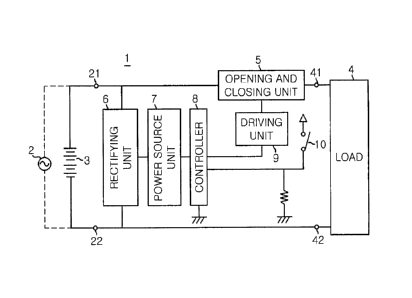
Referring to Fig. 1, the AC/DC two-way switch 1 is
connected between one of an AC power source 2 and a DC power
source 3 and a load 4. The AC/DC two-way switch 1 includes
an opening and closing unit 5 having a bi-directional
semiconductor switch connected in series between a first
input terminal 21 to which one side of the AC power source 2
or a positive electrode side of the DC power source 3 is
connected and a first output terminal 41 to which one end of
the load 4 is connected, and a rectifying unit 6 connected
between the first input terminal 21 and a second input
terminal 22 to which the other side of the AC power source 2
or a negative electrode side of the DC power source 3 is
connected.
Further, the AC/DC two-way switch 1 includes a power
source unit 7 for converting an output voltage from the
-15-
CA 02765943 2011-12-16
rectifying unit 6 into a certain stable voltage, a
controller 8 for controlling an entire operation of the
AC/DC two-way switch 1 by using a power supplied from the
power source unit 7, and a driving unit 9 for driving the
opening and closing unit 5 based on a control signal from
the controller 8. Furthermore, the AC/DC two-way switch 1
includes a manipulation unit 10 installed on a surface of a
wall or the like and operated by a user, and the like. In
Fig. 1, reference numeral 42 denotes a second output
terminal to which the other end of the load 4 is connected.
An internal power source of the AC/DC two-way switch 1
includes the rectifying unit 6 and the power source unit 7.
Thus, when the AC/DC two-way switch 1 is connected with the
AC power source 2, a power is supplied through the
rectifying unit 6. On the other hand, when the AC/DC two-
way switch 1 is connected to the DC power source 3, a power
is directly supplied from the DC power source 3 to the power
source unit 7. And thus, the AC/DC two-way switch 1 can be
used for both of an AC distribution system and a DC
distribution system. Also, the internal power source of the
AC/DC two-way switch 1 is not limited thereto, and another
power source configuration, such as a switching power source
or the like, may be provided.
The manipulation unit 10 may include a mechanical
switch having switching contacts, or a remote control switch
using a low power radio wave or the like based on an
-16-
CA 02765943 2011-12-16
,
infrared ray or electromagnetic wave. Alternatively, the
manipulation unit 10 may include a sensor such as a human
body sensor using a superconductivity effect, a timer, or
the like. Preferably, the manipulation unit 10 outputs a
signal for turning on or off the load 4.
In the present embodiment, the opening and closing
unit 5 includes the bi-directional semiconductor switch
having a transistor structure that does not have direction
dependency on a current or voltage inputted. In this case,
when the positive and the negative electrode of the DC power
source 3 are inversely connected, a current path is cut off
by disconnecting the negative electrode thereof, and,
however, the opening and closing unit 5 remains switchable
(electrically turning on/off). As a result, a switch
function can be secured. Further, as mentioned above, the
opening and closing unit 5 can be connected with either one
of the AC power source 2 and the DC power source 3.
Fig. 2 includes a detailed example of the opening and
closing unit 5 shown in Fig. 1, showing a bi-directional
semiconductor switch formed of inversely-connected elements
of a high voltage-withstanding type vertical transistor
structure. With this structure, the bi-directional
semiconductor switch can be formed by using a switch element
having a general structure, e.g., an easily available and
inexpensive Si-MOSFET or the like. Further, a large
capacitive load may be controlled by using a switch element
-17-
CA 02765943 2014-11-10
such as a low-loss SiC or the like in the above structure.
Fig. 3 shows a detailed example of the opening and
closing unit 5 in which a novel bi-directional semiconductor
switch element 51 in accordance with the present invention
is used. The bi-directional semiconductor switch element 51
is foLmed of a bi-directionally controllable lateral single-
gate transistor element. Fig. 4 is a plan view showing a
configuration of the bi-directional semiconductor switch
element 51, and Fig. 5A is a sectional view taken along a
line A-A shown in Fig. 4.
As shown in Fig. 5A, a substrate 120 of the bi-
directional semiconductor switch element 51 includes a
conductor layer 120a, and a GaN layer 120b and an AlGaN
layer 120c stacked in that order on the conductor layer 120a.
In the bi-directional semiconductor switch element 51, a
two-dimensional (2D) electron gas layer generated at
AlgaN/GaN heterogeneous interface is used as a channel layer.
As shown in Fig. 4, on a surface 120d of the substrate
120, there are provided a first electrode D1 and a second
electrode D2 connected in series with the power source 2 or
3 and the load 4, and an intermediate potential unit S
having an intermediate potential over the potential of the
first electrode D1 and that of the second electrode D2.
Further, a control electrode (gate) G is stacked on top of
the intermediate potential unit S.
As the control electrode G, for example, a Schottky
-18-
CA 02765943 2011-12-16
electrode is used. The first and second electrodes D1 and
D2 have comb-like shapes including multiple electrode units
111, 112, 113,
and 121, 122, 123, arranged in parallel
to each other, respectively. The electrode units arranged
in the comb-like shapes are disposed to face each other.
Further, the intermediate potential unit S and the control
electrode G are disposed between the electrode units 111,
112, 113,
and 121, 122, 123, arranged in the comb-like
shapes, and have approximately fish backbone shapes
corresponding to planar shapes among the electrode units.
The lateral transistor structure included in the bi-
directional semiconductor switch element 51 will now be
described. As shown in Fig. 4, the first and second
electrodes D1 and D2 are arranged in parallel on the surface
120d such that a central line in a width direction of the
electrode unit 111 of the first electrode D1 coincides with
that of the electrode unit 121 of the second electrode D2,
for example. Accordingly, adjacent portions of the
intermediate potential unit S and the control electrodes G
are provided in parallel with the electrode unit 111 of the
first electrode D1 and the electrode unit 121 of the second
electrode D2, respectively.
Herein, a distance to the adjacent intermediate
potential unit S and control electrodes G from the electrode
unit 111 of the first electrode D1 and the electrode unit
121 of the second electrode D2 in the width direction is set
-19-
CA 02765943 2011-12-16
to be a distance from which a certain withstand voltage can
be obtained. In a length direction perpendicular to the
width direction, a distance to the adjacent intermediate
potential unit S and control electrodes G from the ones of
the electrode units of the first electrode D1 and the second
electrode D2 is set similarly.
Further, these relationships are similar for the other
electrode units 112 and 122, 113, and 123, _ . In other
words, the intermediate potential unit S and the control
electrodes G are disposed at positions at which a certain
withstand voltage can be obtained with respect to the first
and second electrodes D1 and D2.
In the present embodiment, the intermediate potential
unit S having an intermediate potential with respect to the
potentials of the first electrode D1 and the second
electrode D2 and the control electrode G connected to the
intermediate potential unit S to control the intermediate
potential unit S are disposed at positions at which acertain
withstand voltage can be obtained with respect to the first
electrode D1 and the second electrode D2. Thus, for example,
in case where the first electrode D1 is at a high potential
side and the second electrode D2 is at a low potential side,
when the bi-directional semiconductor switch element 51 is
turned off and a signal of OV is applied to the control
electrode G, a current is reliably cut off at least among
the first electrode D1, and the control electrode G and the
-20-
CA 02765943 2011-12-16
intermediate potential unit S, i.e., a current is blocked
immediately below the control electrode (gate) G.
Meanwhile, when the bi-directional semiconductor
switch element 51 is turned on and a signal having a voltage
of a certain threshold or higher is applied to the control
electrode G, a current flows along a path from the first
electrode D1 (electrode units 111, 112, 113, _), through the
intermediate potential unit S, to the second electrode D2
(electrode units 121, 122, 123,_) as indicated by arrows in
Fig. 4 and this holds true for the reversed case, too.
As described above, the intermediate potential unit S
is formed at the position at which the certain withstand
voltage can be obtained with respect to the first electrode
D1 and the second electrode D2. Therefore, even when a
threshold voltage of a signal applied to the control
electrode G is lowered to the lowest level required, the bi-
directional semiconductor element 51 can be reliably turned
on and off, thereby realizing a low on-resistance. Also, by
having the opening and closing unit 5 to be formed of the
bi-directional semiconductor switch element 51 and making a
reference (GND) of the control signal have the same
potential as that of the intermediate potential unit S, the
DC power source 3 or the AC power source 2 of a high voltage
can be controlled by the controller 8 which can be driven by
a control signal of a few volts.
Further, in the lateral transistor element using the
-21-
CA 02765943 2011-12-16
2D electron gas layer generated at the heterogeneous
interface as a channel layer, there is a reciprocal
relationship between high potentialization of the threshold
voltage that makes the element electrically non-conductive
and ON-resistance in conducting.
Therefore, when the
threshold voltage is lowered, ON-resistance can become a low
level, which makes it possible to realize the AC/DC two-way
switch 1 to be of a high capacity at a small scale.
Fig. 6 shows a modified example of the configuration
illustrated in Fig. 3. In
the configuration example
illustrated in Fig. 3, the bi-directional controllable
lateral single-gate transistor element is used as the bi-
directional semiconductor switch element 51, and a full-wave
rectification circuit is used in the rectifying unit 6. In
the example illustrated in Fig. 6, a bi-directional
controllable lateral dual-gate transistor element is used as
the bi-directional semiconductor switch element 51 and a
half-wave rectification circuit is used as the rectifying
unit 6.
As shown in Fig. 5B, the lateral dual-gate transistor
element includes a first electrode D1 and a second electrode
D2 connected in series with the power source 2 or 3 and the
load 4 and formed on the surface of the substrate 120, and a
first control electrode (first gate electrode) G1 and a
second control electrode (second gate electrode) G2 each
receiving an independent control signal, at least a portion
-22-
CA 02765943 2011-12-16
of each of the first and the second control electrode G1 and
G2 being formed on the surface of the substrate 120.
Each of the first control electrode G1 and the second
control electrode G2 is disposed at a position at which a
certain withstand voltage can be obtained.
Since the
withstand voltage is needed at one portion, a bi-directional
element with a low loss can be realized. The element having
this configuration is controlled based on the voltages of
drain electrodes D1 and D2 as respective references, and
different driving signals are inputted to the two gate
electrodes G1 and G2, respectively (for that reason, the
element is called a dual gate transistor structure).
Referring to Fig. 6 again, an anode of a diode 61 is
connected to a first input terminal 21 to which the positive
electrode of the DC power source 3 is connected. When the
AC/DC two-way switch 1 is connected with the AC power source
2, a power is normally supplied to the controller 8 through
the rectifying unit 6, i.e., either the full-wave
rectification circuit or the half-wave rectification circuit
as the rectifying unit 6, and the power source unit 7.
Meanwhile, in case where the AC/DC two-way switch 1 is
connected with the DC power source 3 and the half-wave
rectification circuit is used as the rectifying unit 6, when
the positive electrode and the negative electrode of the DC
power source 3 are inversely erroneously wired, a power is
not supplied to the controller 8. Accordingly, the AC/DC
-23-
CA 02765943 2011-12-16
two-way switch 1 does not operate, and a power is not
supplied to the load 4. As a result, it is possible to
recognize that the element is erroneously connected in
wiring.
In the modified example shown in Fig. 6, a diode 62 is
connected to the second input terminal 22 to which the
negative electrode of the DC power source 3 is connected as
well. However, the operation is similarly performed even
when the diode 61 is connected only to the first input
terminal 21 to which the positive electrode of the DC power
source 3 is connected.
In the present embodiment, the driving unit 9 has an
insulating structure such as a transformer or the like in
which a primary side thereof is connected with the
controller 8 and a secondary side thereof is connected with
the control electrodes G1 and G2 of the bi-directional
semiconductor switch element 51. When a signal for turning
on the load 4 is received from the manipulation unit 10, the
controller 8 supplies a certain power to the primary side of
the transformer of the driving unit 9. Then, a certain
voltage is induced at the secondary side of the transformer.
Accordingly, a control voltage is applied to the
control electrodes G1 and G2 of the bi-directional
semiconductor switch element 51 based on the induced voltage,
thereby electrically conducting (closing) the bi-directional
semiconductor switch element 51, i.e., the opening and
-24-
CA 02765943 2011-12-16
closing unit 5. Herein, since the primary side and the
secondary side of the transformer are insulated, the
controller 8 may make a high voltage be applied or a large
current flow through the opening and closing unit 5 without
damage. Further, the insulating structure is not limited to
the transformer and may use a light emitting element and a
light receiving element such as a photo-coupler, or the like.
Fig. 7 shows a configuration including a power type
determination unit 71 and a power type informing unit 72. A
detailed configuration and a determination method of the
power type determination unit 71 are not particularly
limited. For example, the controller 8 may compare a
threshold with an analog value obtained by stepping down an
input voltage by a certain magnification. Alternatively, a
filter or the like including a condenser, a coil or the like
may be used to split a DC and an AC. Further, a detailed
configuration and method of the power type informing unit 72
are not also particularly limited. For example, two LEDs
each having a different light emitting color may be used in
which LEDs for lighting are switched depending on an AC or a
DC, or a single LED may be used in which the LED is switched
between lighting constantly and flickering depending on an
AC or a DC.
As the above, since the power type determination unit
71 and the power type informing unit 72 are provided, even
in the distribution system in which the AC power source 2
-25-
CA 02765943 2011-12-16
and the DC power source 3 coexist, the types of the power
sources connected with respective switches can be recognized,
thereby facilitating user's recognition and making
maintenance easier.
Fig. 8A shows a detailed example of the power type
determination unit 71 in which a zero cross of an input
voltage is detected. As shown in Fig. 8A, an input voltage
from the rectifying unit 6 is divided by resistors 73 and 74,
and the divided voltage is applied between an emitter and a
base of the transistor 75. And, the controller 8 monitors a
terminal voltage of a collector of the transistor 75. When
the AC/DC two-way switch 1 is connected with the AC power
source 2, a ripple current rectified by the rectifying unit
6 is inputted to the power type determination unit 71.
When the input voltage is greater than a threshold
value of the transistor 75, the transistor 75 is turned on,
and the terminal voltage of the collector becomes lower than
a determination threshold value (LOW). Meanwhile, when the
input voltage is smaller than the threshold value of the
transistor 75, the transistor 75 is turned off and the
terminal voltage of the collector becomes higher than the
determination threshold value (HIGH)(see Fig. 8B).
Thus,
the power type determination unit 71 outputs a detect signal
(pulse) only during a certain period of time before and
after the input voltage is zero-crossed.
On the other hand, when the AC/DC two-way switch 1 is
-26-
CA 02765943 2011-12-16
connected with the DC power source 3, the input voltage is
constant as shown in Fig. 8C. Accordingly, the transistor
75 is kept in an ON state and the terminal voltage of the
collector constantly has a value lower than the
determination threshold value (constantly LOW). Thus, if
the terminal voltage of the collector periodically becomes
higher than the threshold value, it may be determined that
the AC/DC two-way switch 1 is connected with the AC power
source 2. With the present embodiment detecting the zero-
cross, the circuit configuration can be simplified, the
controller 8 can make determination based on a digitized
signal, and the controller 8 can easily perform processing.
As shown in Fig. 8D, a timing for turning on the bi-
directional semiconductor switch element 51 (i.e., a timing
for driving the driving unit 9) may be set to be in
synchronization with a zero-cross detection by the power
type determination unit 71, other than an ON signal from the
manipulation unit 10. By doing so, since the bi-directional
semiconductor switch element 51 is electrically connected at
a low voltage level, an inrush current can be reduced.
Fig. 9 illustrates a configuration in which an
auxiliary switch element 52 having mechanical switching
contacts is connected in parallel to the bi-directional
semiconductor switch element 51 as the opening and closing
unit 5. As for the auxiliary switch element 52, for example,
a relay or the like may be used. When the controller 8
-27-
CA 02765943 2011-12-16
supplies a certain power to the driving unit 9 or outputs a
certain driving signal, the opening and closing unit 5
becomes conductive. After the bi-directional semiconductor
switch element 51 of the opening and closing unit 5 becomes
conductive, the auxiliary switch element 52 becomes
conductive.
In the present embodiment, by using the auxiliary
switch element 52 such as a relay or the like having high
electrical conductivity, the capacity of a load current can
be considerably increased. When the opening and closing
unit 5 is made non-conductive, the controller 8 first opens
the auxiliary switch element 52 and then makes the bi-
directional semiconductor switch element 51 non-conductive.
Accordingly, the switching contacts of the auxiliary switch
element 52 are open in a state that the bi-directional
semiconductor switch element 51 is electrically connected
(i.e., both ends of the auxiliary switch element 52 are
equi-potential). As a result, there develops no arc used to
occur in the DC power source 3, thereby preventing a life
span problem due to a degradation of the switching contacts.
Fig. 10 shows a configuration in which an auxiliary
switch element 53 having mechanical switching contacts is
connected in series with the bi-directional semiconductor
switch element 51 included in the opening and closing unit 5.
The auxiliary switch element 53, e.g., a relay or the like
may be used. When the opening and closing unit 5 is made
-28-
CA 02765943 2011-12-16
conductive, the controller 8 supplies a certain power to the
driving unit 9, or outputs a certain driving signal. In
this case, after the switching contacts of the auxiliary
switch element 53 in the opening and closing unit 5 are
connected, the bi-directional semiconductor switch element
51 is made conductive.
Further, when the opening and closing unit 5 is made
non-conductive, the controller 8 first makes the bi-
directional semiconductor switch element 51 of the opening
and closing unit 5 non-conductive and then disconnects the
auxiliary switch element 53. Accordingly, the opening and
closing unit 5 becomes completely non-conductive, and no
current flows into the load 4. That is, when the AC/DC two-
way switch 1 is turned off, the load 4 is insulated.
Fig. 11 illustrates a configuration including a
communications function unit (or a signal reception unit) 81
for transmitting and receiving a signal to and from an
external device 82 such as a remote controller device or the
like. Fig. 12 represents a modified example from that shown
in Fig. 11 in which a control signal from an external device
83 connected to a power line is overlapped with the power to
be transmitted, and the control signal is detected by a
signal detection unit 84.
With these configurations, a user can remotely or
automatically control ON/OFF operation of the load 4 such as
a lighting apparatus or the like, without, for example,
-29-
CA 02765943 2011-12-16
directly having to manipulate the manipulation unit 10
provided on the wall. With the configuration shown in Fig.
12, there is no need to provide a dedicated communications
line or a wireless transceiver.
Fig. 13 depicts a configuration in which two opening
and closing units 5 are provided at both sides of a power
line. With this configuration, a driving signal is
simultaneously supplied to the two bi-directional
semiconductor switch elements 51 through the driving unit 9
having the insulating structure, and the degree of freedom
in the installation of the two bi-directional semiconductor
switch elements 51 increases. Further, since the opening
and closing units 5 are provided at two portions, it is
possible to provide a switch usable in a power system such
as an AC 200 V system or a photovoltaic power generation
system generating DC 300 V, or the like in which it has a
higher voltage to ground and a power line has multiple
short-circuited portions. For example, although not shown,
the bi-directional semiconductor switch element as an
opening and closing unit may be provided at each line of a
single-phase three-wire or a three-phase power source, the
three opening and closing units being simultaneously opened
and closed.
Referring to Fig. 14, a configuration is shown in
which the AC/DC two-way switch 1 has a socket unit, rather
than being directly connected with the load 4. With this
-30-
CA 02765943 2011-12-16
configuration, a load such as a portable lighting apparatus
or the like can be controlled. The AC/DC two-way switch 1
may be formed of an adapter type switch which can be
inserted into an existing socket or may be buried in the
wall. In this case, the first output terminal 41 and the
second output terminal 42 of the output side may have a
general socket shape.
Figs. 15A and 15B show configurations in which the
rectifying units 6 and the power source units 7 both are
provided at an input side and an output side of the AC/DC
two-way switch 1. With this configuration, the input side
and the output side of the AC/DC two-way switch 1 are not
limited, and the AC/DC two-way switch 1 may serve as a
switch no matter where the load or a power source is
connected. For example, the AC/DC two-way switch 1 may be
applied to a system in which a load itself also serves as a
power source, such as a system in which a storage battery is
used as the DC power source 3 and a motor is controlled as
the load 4. Specifically, the motor is driven by power from
the storage battery, but the motor generates a power as a
generator when the motor is idle. In this case, the motor
is a power source and the storage battery is a load, and the
storage battery can be charged from the power generated by
the motor.
As described above, the AC/DC two-way switch 1 in
accordance with the above embodiments uses the bi-
-31-
CA 02765943 2011-12-16
directional semiconductor switch element 51, as a switch
element included in the opening and closing unit, which does
not have direction dependency with respect to an input
current or voltage. Accordingly, the AC/DC two-way switch 1
can be used in either an AC distribution system or a DC
distribution system. Further, when the AC/DC two-way switch
1 is used in the DC distribution system, the AC/DC two-way
switch can be opened and closed without generating an arc
because of the bi-directional semiconductor switch element.
As a result, a device for extinguishing an arc is not
required and the AC/DC two-way switch 1 can be substituted
for a switch for an existing AC distribution system by
reducing the size of the semiconductor element.
Furthermore, the present invention is not limited to
the configurations of the forgoing embodiments and, of
course, the configuration examples as illustrated may be
arbitrarily combined.
-32-