Note: Descriptions are shown in the official language in which they were submitted.
CA 02766545 2012-02-01
38331caf
SENSING APPARATUS AND SENSING METHOD
BACKGROUND
Technical Field
[0001] The disclosure relates to a sensing apparatus and a sensing method.
Related Art
[0002] With development of sensing techniques, flat-type sensing unit arrays
have
been widely applied in various domains, for example, applied in optical image
sensors,
digital radiography sensors (DRS) and touch screen sensors, etc. A structure
of a main
device (an active array substrate) of the flat-type sensing unit array is
similar to a
substrate in a flat panel display, for example, similar to a thin-film
transistor array
substrate in a thin film transistor liquid crystal display (TFT-LCD).
[0003] In order to further improve a sensing effect, the current sensing
technique is
developed towards a trend of large area sensing, improvement of a low-energy
sensing
capability and high resolution. However, enhancement of the resolution may
reduce a
pixel area of a sensor, and accordingly reduce sensitivity of the sensor for
sensing an
incident energy. Moreover, low incident energy may result in a low strength of
an
electric signal converted from the energy by the sensor. Moreover, the large
area
sensing is liable to generate noises due to resistance and capacitance (RC)
coupling of
the sensor.
[0004] Generally, one pixel on the conventional active array substrate only
contains
a single thin film transistor to serve as a switch for read and reset
operations, and such
structure cannot achieve signal gain to mitigate the noise problem. A
conventional
1
CA 02766545 2012-02-01
38331caf
design that has a pixel amplifier can only resolve a part of the
aforementioned problems,
and cannot resolve all of the aforementioned problems.
SUMMARY
[0005] An embodiment of the disclosure provides a sensing apparatus including
a
first scan line, a second scan line, a readout line, a first sensing unit, and
a second
sensing unit. The first sensing unit is coupled to the first scan line, the
second scan
line, and the readout line and is configured to sense a first energy. The
first sensing
unit outputs a first readout signal corresponding to the first energy to the
readout line in
response to a first scan signal on the first scan line. The second sensing
unit is coupled
to the second scan line and the readout line and is configured to sense a
second energy.
The second sensing unit outputs a second readout signal corresponding to the
second
energy to the readout line in response to a second scan signal on the second
scan line.
The second scan signal works in cooperation with the first scan signal to
reset the first
sensing unit.
[0006] Another embodiment of the disclosure provides a sensing method
including
following steps. A first sensing unit and a second sensing unit are provided
to
respectively sense a first energy and a second energy. The first sensing unit
outputs a
first readout signal corresponding to the first energy in response to a first
scan signal.
The second sensing unit outputs a second readout signal corresponding to the
second
energy in response to a second scan signal. The second scan signal works in
cooperation with the first scan signal to reset the first sensing unit.
[0007] In order to make the aforementioned and other features and advantages
of
the disclosure comprehensible, several exemplary embodiments accompanied with
2
CA 02766545 2012-02-01
38331caf
figures are described in detail below.
BRIEF DESCRIPTION OF THE DRAWINGS
[0008] The accompanying drawings are included to provide a further
understanding
of the disclosure, and are incorporated in and constitute a part of this
specification.
The drawings illustrate embodiments of the disclosure and, together with the
description,
serve to explain the principles of the disclosure.
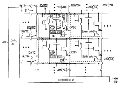
[0009] FIG. I is a circuit schematic diagram of a sensing apparatus according
to an
exemplary embodiment.
[0010] FIG. 2 is a waveform diagram of the sensing apparatus of FIG. 1.
[0011] FIG. 3 shows an example of the sensing device in FIG. 1.
[0012] FIG. 4 is a partial circuit diagram of the interpretation unit of FIG.
1.
[0013] FIG. 5 is a flowchart illustrating a sensing method according to an
exemplary embodiment.
DETAILED DESCRIPTION OF DISCLOSED EMBODIMENTS
[0014] Below, exemplary embodiments will be described in detail with reference
to
accompanying drawings so as to be easily realized by a person having ordinary
knowledge in the art. The inventive concept may be embodied in various forms
without
being limited to the exemplary embodiments set forth herein. Descriptions of
well-known parts are omitted for clarity, and like reference numerals refer to
like
elements throughout.
[0015] FIG. 1 is a circuit schematic diagram of a sensing apparatus according
to an
exemplary embodiment, and FIG. 2 is a waveform diagram of the sensing
apparatus of
3
CA 02766545 2012-02-01
38331 caf
FIG. 1. Referring to FIG. 1 and FIG. 2, the sensing apparatus 100 of the
embodiment
includes a plurality of scan lines 110, a plurality of readout lines 120 and a
plurality of
sensing units 200. In FIG. 1, three scan lines l 10a, I10b and 110c, three
readout lines
120a, 120b and 120c, and four sensing units 200a, 200b, 200c and 200d are
schematically illustrated for example, and in the present embodiment, circuit
structures
of the sensing units 200, the scan lines 110 and the readout lines 120 can
repeatedly
appear at top, bottom, left and right of FIG. 1. For example, regarding the
scan lines
110, a first scan line 110, a second scan line 110, ..., a Kth scan line 110
are sequentially
arranged from the top to the bottom in FIG. 1, where K is a positive integer
greater than
or equal to 3. Scan lines 110a, I10b and I10c shown in FIG. 1 are respectively
an Nth
scan line 110, an (N+1)th scan line 110 and an (N+2)th scan line 110, where N
is a
positive integer smaller than or equal to K-2. Regarding the readout lines
120, a first
readout line to a ph readout line are sequentially arranged from the left to
the right in
FIG. 1, where J is a positive integer greater than or equal to 2. Readout
lines 120a,
120b and 120c shown in FIG. I are respectively an (M-1)th readout line 120, an
Mtn
readout line 120 and an (M+I)th readout line 120, where M is a positive
integer smaller
than or equal to J-1. When J=2, the readout line 120a can be removed. Each of
the
sensing units 200 is coupled to two adjacent scan lines 110, and is coupled to
one
adjacent readout line 120. For example, the sensing unit 200a is coupled to
the scan
line I IOa, the scan line I IOb and the readout line 120b, and the sensing
unit 200b is
coupled to the scan line 110b, the scan line I IOc and the readout line 120b.
Moreover,
each of the sensing units 200 is configured to sense an energy E exerted
thereon. For
example, the sensing unit 200a is configured to sense an energy E1, and the
sensing unit
200b is configured to sense an energy E2.
4
CA 02766545 2012-02-01
38331caf
[0016] The sensing unit 200a outputs a readout signal RI corresponding to the
energy E 1 to the readout line 120b in response to a scan signal 112a on the
scan line
110a. The sensing unit 200b outputs a readout signal R2 corresponding to the
energy
E2 to the readout line 120b in response to a scan signal 112b on the scan line
11 Ob.
Moreover, the scan signal 112b works in cooperation with the scan signal 112a
to reset
the sensing unit 200a. Moreover, a scan signal I 12c on the scan line 110c
works in
cooperation with the scan signal 112b to reset the sensing unit 200b.
[0017] In present embodiment, each of the sensing units 200 (for example, the
sensing unit 200a, 200b, 200c or 200d) includes a sensing device 210, a
storage device
220, an amplification device 230 and a reset device 240. The sensing device
210
senses the energy E, and converts the sensed energy E into a data signal. The
storage
device 220 is coupled to the adjacent scan line 110 and the sensing device
210, and is
configured to store the data signal. For example, the sensing device 210 of
the sensing
unit 200a senses the energy El, and converts the sensed energy El into a data
signal,
and the storage device 220 of the sensing unit 200a is coupled to the scan
line 11 Oa and
the sensing device 210 of the sensing unit 200a, and is configured to store
the data
signal converted from the energy E1.
[0018] The amplification device 230 is coupled to the storage device 220, the
adjacent scan line 110 and the adjacent readout line 120, where the
amplification device
230 outputs the readout signal R corresponding to the data signal to the
readout line 120
in response to the scan signal 112 on the adjacent scan line 110. Moreover,
the reset
device 240 is coupled to the storage device 220, the aforementioned adjacent
scan line
110 and another adjacent scan line 110 (i.e. a next-stage scan line 110), and
the reset
device 240 resets the storage device 220 in response to the scan signal 112 on
the
5
CA 02766545 2012-02-01
38331caf
adjacent scan line 110 (for example, the scan line 110 on the top of the reset
device 240
in FIG. 1) and the scan signal 112 on the other adjacent scan line 110 (i.e.
the next-stage
scan line 110, for example, the scan line 110 at the bottom of the reset
device 240 in
FIG. 1).
[0019] For example, the amplification device 230 of the sensing unit 200a is
coupled to the storage device 220 of the sensing unit 200a, the scan line I
IOa and the
readout line 120b, where the amplification device 230 of the sensing unit 200a
outputs
the readout signal R corresponding to the data signal stored in the storage
device 220 of
the sensing unit 200a to the readout line 120b in response to the scan signal
112a on the
scan line 110a. Moreover, the reset device 240 of the sensing unit 200a is
coupled to
the storage device 220 of the sensing unit 200a, the scan line 1 IOa and the
scan line
110b, and the reset device 240 of the sensing unit 200a resets the storage
device 220 of
the sensing unit 200a in response to the scan signal 112b on the scan line
110b and the
scan signal 112a on the scan line I I Oa.
[0020] In the present embodiment, in each of the sensing units 200, the energy
E is
light energy or electromagnetic energy, and the sensing device 210 is an
electromagnetic sensing device, for example, a photodiode. However, in another
embodiment, the electromagnetic sensing device can also be a photoresistor, a
photoconductor, a phototransistor, or other suitable electromagnetic sensing
devices.
Moreover, in other embodiments, the energy E can also be a mechanical energy,
for
example, an elastic potential energy, or a kinetic energy, etc., and the
sensing device
210 is, for example, a pressure sensing device. The pressure sensing device
is, for
example, a piezoelectric sensor or other suitable pressure sensing devices. In
addition,
the energy E can also be thermal energy, and the sensing device 210 is, for
example, a
6
CA 02766545 2012-02-01
38331caf
temperature sensing device. Moreover, the energy E can also be electric
energy, and
the sensing device 210 is, for example, a touch sensing device for sensing
capacitance
variation caused by a touch operation of a finger or other objects. In the
other
embodiments, the energy E can also be other types of energy that can be
detected, and
the sensing device 210 is a corresponding sensor for detecting such energy.
[0021] In the present embodiment, a current input terminal Ti of the
amplification
device 230 of the sensing unit 200a is coupled to the scan line 110a and a
first terminal
T4 of the storage device 220 of the sensing unit 200a, a control terminal T2
of the
amplification device 230 of the sensing unit 200a is coupled to a second
terminal T5 of
the storage device 220 of the sensing unit 200a, and a current output terminal
T3 of the
amplification device 230 of the sensing unit 200a is coupled to the readout
line 120b.
The amplification device 230 is, for example, a transistor. In the present
embodiment,
the amplification device 230 in each of the sensing units 200 is, for example,
a field
effect transistor, and the current input terminal Ti, the control terminal T2
and the
current output terminal T3 are, for example, respectively a source, a gate and
a drain of
the field effect transistor. However, in other embodiments, the amplification
device
230 can also be a bipolar transistor or other transistors. In the present
embodiment, the
storage device 220 of each of the sensing units 200 is, for example, a
capacitor, and a
capacitance of the capacitor is far greater than a parasitic capacitance
(typically about or
more than 0.055 pF) between the current input terminal TI and the control
terminal T2
of the amplification device 230. In an embodiment, the capacitance of the
capacitor is
greater than or equal to 0.55 pF, or the capacitance of the capacitor is
greater than or
equal to 10 times of the parasitic capacitance between the current input
terminal Ti and
the control terminal T2 of the amplification device 230.
7
CA 02766545 2012-02-01
38331caf
[0022] In the present embodiment, a first terminal T6 of the reset device 240
of the
sensing unit 200a is coupled to the scan line 11 Oa, a control terminal T7 of
the reset
device 240 of the sensing unit 200a is coupled to the scan line 11Ob, and a
second
terminal T8 of the reset device 240 of the sensing unit 200a is coupled to the
control
terminal T2 of the amplification device 230 of the sensing unit 200a. In the
present
embodiment, the reset device 240 in each of the sensing units 200 is, for
example, a
field effect transistor, and the first terminal T6, the control terminal T7
and the second
terminal T8 thereof are, for example, respectively a source, a gate and a
drain of the
field effect transistor. However, in other embodiments, the reset device 240
can also
be a bipolar transistor, other transistors or other switch devices.
[0023] In the present embodiment, the sensing device 210 of the sensing unit
200b
senses the energy E2, and converts the sensed energy E2 into a data signal.
The
storage device 220 of the sensing unit 200b is coupled to the scan line I IOb
and the
sensing device 210 of the sensing unit 200b, and is configured to store the
data signal
converted from the energy E2. The amplification device 230 of the sensing unit
200b
is coupled to the storage device 220 of the sensing unit 200b, the scan line 1
l0b and the
readout line 120b, where the amplification device 230 outputs a readout signal
R2
corresponding to the data signal converted from the energy E2 to the readout
line 120b
in response to the scan signal I 12b on the scan line 110b.
[0024] Moreover, in this embodiment, the reset device 240 of the sensing unit
200b
is coupled to the storage device 220 of the sensing unit 200b, the scan line
11Ob and the
scan line 110c, and the reset device 240 of the sensing unit 200b resets the
storage
device 220 of the sensing unit 200b in response to a scan signal 112c on the
scan line
I IOc and the scan signal 112b on the scan line 110b.
8
CA 02766545 2012-02-01
38331caf
[0025] In detail, in the present embodiment, the current input terminal Ti of
the
amplification device 230 of the sensing unit 200b is coupled to the scan line
I IOb and
the first terminal T4 of the storage device 220 of the sensing unit 200b, the
control
terminal T2 of the amplification device 230 of the sensing unit 200b is
coupled to the
second terminal T5 of the storage device 220 of the sensing unit 200b, and the
current
output terminal T3 of the amplification device 230 of the sensing unit 200b is
coupled
to the readout line 120b. Moreover, the first terminal T6 of the reset device
240 of the
sensing unit 200b is coupled to the scan line 110b, the control terminal T7 of
the reset
device 240 of the sensing unit 200b is coupled to the scan line 11Oc, and the
second
terminal T8 of the reset device 240 of the sensing unit 200b is coupled to the
control
terminal T2 of the amplification device 230 of the sensing unit 200b.
[0026] In the present embodiment, the scan signals 112 sequentially enable the
sensing units 200. For example, the scan signal 112a, the scan signal 112b and
the
scan signal 112c sequentially enable the sensing unit 200a, the sensing unit
200b and a
next-stage sensing unit of the sensing unit 200b (not shown). In the present
embodiment, the scan signals 112 are sent from a driving unit 300, and the
driving unit
300 is electrically connected to the scan lines 110. The driving unit 300 is,
for
example, a driving circuit.
[0027] In the present embodiment, when the scan signal 112 of a scan line 110
has a
high voltage level VH, the scan signal 112 causes conduction between the first
terminal
T6 and the second terminal T8 of the reset device 240 in the previous-stage
sensing unit
200 relative to the scan line 110, and now the scan signal 112 of the previous-
stage scan
line 110 has a low voltage level VL, so that the first terminal T4 and the
second terminal
T5 of the storage device 220 of the previous-stage sensing unit 200 are all in
the low
9
CA 02766545 2012-02-01
38331caf
voltage level VL to reset the storage device 220. For example, in a time
period P3 of
FIG. 2, the scan signal I 12a on the scan line 110a has the low voltage level
VL, and the
scan signal 112b on the scan line I IOb has the high voltage level VH, and now
the scan
signal 112b is transmitted to the control terminal T7 of the reset device 240
to turn on
the reset device 240, so that a node 205a has a voltage level the same as the
low voltage
level VL of the scan signal 112a. In this way, the scan line I IOa and the
node 205a are
all in the low voltage level VL, and the storage device 220 substantially has
no charge
accumulation, so as to achieve an effect that the scan signal 112b works in
cooperation
with the scan signal 112a to reset the storage device 220. Now, the control
terminal
T2 of the amplification device 230 is also in the low voltage level VL, so
that the
amplification device 230 is turned off, and the current output terminal T3 of
the
amplification device 230 does not output a current signal to the readout line
120b.
[0028] After the time period P3, for example, in a time period P4, the scan
signal
112a and the scan signal 112b are all in the low voltage level VL, so that the
reset device
240 is turned off. Now, the node 205a is still maintained to a final state as
that in the
time period P3, i.e. the low voltage level VL.
[0029] FIG. 3 shows an example of the sensing device in FIG. 1. Referring to
FIG.
1 to FIG. 3, the sensing device 210 in FIG. 3 is, for example, a photodiode.
An N-pole
of the photodiode is coupled to the node 205, where the node 205 is coupled
between
the second terminal T8 of the reset device 240 and the control terminal T2 of
the
amplification device 230, and is coupled between the second terminal T5 of the
storage
device 220 and the N-pole of the photodiode. Moreover, a P-pole of the
photodiode is
coupled to a terminal 206. In a time period P1 after the time period P4 in
FIG. 2, a
negative voltage is applied on the terminal 206. Now, the scan signal 112a on
the scan
CA 02766545 2012-02-01
38331caf
line I IOa and the scan signal 112b on the scan line 110b are all in the low
voltage level
VL, so that the node 205a is still in the low voltage level VL. Therefore, the
sensing
device 210 (i.e. the photodiode) of the sensing unit 200a withstands a reverse
bias.
Now, when light irradiates the sensing device 210 of the sensing unit 200a
(i.e. the
sensing device 210 receives the energy E), a reverse current flowing through
the sensing
device 210 is generated, i.e. a current flowing from the node 205 (i.e. the
node 205a) to
the terminal 206, so that the charges are accumulated on the storage device
220 of the
sensing unit 200a. In other words, the time period P1 is a sensing time period
of the
sensing unit 200. In this way, a voltage difference A VI is formed between the
second terminal T5 and the first terminal T4 of the storage device 220 of the
sensing
unit 200a. Since now the scan line 110a is still maintained to the low voltage
level VL,
when the time period P1 is ended, the voltage of the node 205a is maintained
to VL+ A
V 1. In the present embodiment, the voltage difference AV 1, for example, has
a
negative value.
[0030] In a time period P2 after the time period P1, the scan signal 112a of
the scan
line I I Oa is in the high voltage level VH, and the scan signal i i 2b of the
scan line i i Ob
is in the low voltage level VL. Now, the scan signal 112b makes the control
terminal
T7 of the reset device 240 of the sensing unit 200a be in the low voltage
level VL, so
that the reset device 240 is turned off. On the other hand, the scan signal
112a pulls up
the voltage level of the node 205a to a voltage level VH' slightly lower than
the high
voltage level VH through a capacitance coupling effect of the storage device
220 of the
sensing unit 200a. In an ideal state, according to the capacitance coupling
effect, a
voltage variation A V2 of the scan signal 112a increased from the low voltage
level VL
to the high voltage level VH is substantially equal to a voltage variation A
V2' of the
11
CA 02766545 2012-02-01
38331caf
node 205a increased from the voltage level VL+ A VI to the voltage level VH'.
However, in an actual application, the voltage variation A V2' is slightly
less than the
voltage variation A V2, and a relationship of the v oltage variation A V2' and
the
voltage variation A V2 is, for example, as follows.
4V = K Cs` AV
2
2 Cs, +C 9
where Cst is a capacitance of the storage device 220, Cg is a gate capacitance
of the amplification device 230 (including a capacitance Cox of a gate oxide
layer or an
insulation layer, a parasitic capacitance Cgs from the gate to the source, and
a parasitic
capacitance Cgd from the gate to the drain), K is a unitless constant, which
is used for
representing other coupling loss, where K<_ 1, and K=I represents no coupling
loss.
[0031] In the ideal state, since the voltage variation A V2' is substantially
equal to
the voltage variation A V2, a voltage difference A V l' of the voltage level
VH' and the
high voltage level VH is substantially equal to the voltage difference A V 1.
However,
in an actual application, an absolute value of the voltage difference A V 1'
is slightly
greater than an absolute value of the voltage difference A VI, and a
relationship
therebetween can be deduced from the above relationship of the voltage
variation A
V2' and the voltage variation A V2.
[0032] When the sensing device 210 of the sensing unit 200a does not sense the
energy E during the time period P1, the current flowing through the sensing
device 210
is not generated, and no charge is accumulated on the storage device 220. In
other
words, a cross voltage of the storage device 220 is 0, i.e. the voltage level
of the node
205a is now in the low voltage level VL. Therefore, in the time period P2
after the
12
CA 02766545 2012-02-01
38331caf
time period P1, in the ideal state, since the scan signal 112a is in the high
voltage level
VH, the node 205a is also in the high voltage level VH through the capacitance
coupling
effect of the storage device 220. Now, due to the amplification effect of the
amplification device 230 of the sensing unit 200a, the high voltage level VH
of the node
205a is converted into a current I flowing from the current input terminal TI
to the
current output terminal T3 of the amplification device 230. However, when the
sensing device 210 of the sensing unit 200a senses the energy E during the
time period
P1, different magnitudes of the sensed energy E may produce different voltage
differences AV 1 at the two ends of the storage device 220 of the sensing unit
200a.
Therefore, in the time period P2 after the time period P1, different voltage
differences
A V 1' are produced. Due to the amplification effect of the amplification
device 230 of
the sensing unit 200a, the voltage level VH+ A VI I of the node 205a is
converted into a
current 1+ A I flowing from the current input terminal Ti to the current
output terminal
T3 of the amplification device 230, where a value of A I corresponds to a
value of A
V l', so that different voltage differences A VI I correspond to different
current
differences A I.
[0033] The current I or the current 1+ A I flows to the readout line 120b
during the
time period P2, and then flows to an interpretation unit 400. The
interpretation unit
400 is electrically connected to the readout lines 120 to interpret the
current signals (i.e.
the readout signals R) received from the readout lines 120. When the current
from the
readout line 120 is the current I, the interpretation unit 400 determines that
the sensing
device 210 of the sensing unit 200 that outputs such current does not sense
the energy E.
When the current from the readout line 120 is the current 1+ A I, the
interpretation unit
13
CA 02766545 2012-02-01
38331caf
400 determines a magnitude of the energy E sensed by the sensing device 210 of
the
sensing unit 200 that outputs such current according to an absolute value of A
I, where
the greater the absolute value of o I is, the greater the energy E sensed by
the sensing
device 210 is. Since the scan signals 112 of the scan lines 110 sequentially
enable the
sensing units 200, the sensing units 200 of different rows (for example, the
sensing unit
200a and the sensing unit 200b) sequentially output the current signals to the
interpretation unit 400. Therefore, the interpretation unit 400 can determine
from
which row of the sensing units 200 the current signals are according to a
receiving time
of the current signals. On the other hand, the sensing units 200 in the same
row (for
example, the sensing unit 200a and the sensing unit 200c) are simultaneously
driven by
the scan signal 112 of the same scan line 110, and the sensing units 200 in
the same row
simultaneously output the current signals to the different readout lines 120.
Therefore,
the interpretation unit 400 can determine from which column of the sensing
units 200
the current signal is according to which of the readout lines 120 the current
signal is
from. Therefore, one sensing unit 200 can be regarded as a pixel, and after
passing
through the time period P1, the time period P2, the time period P3 and the
time period
P4, or further after passing through an enable time of the other scan signals
112 between
the time period P1 and the time period P2 and an enable time of the other scan
signals
112 between the time period P4 and a next time period P1, the sensing
apparatus 100
can extract an image of one frame. Moreover, as the above time periods
repeatedly
appear, the sensing apparatus 100 can extract a plurality of frames, so as to
obtain
dynamic images.
[0034] The other detailed operation of the sensing unit 200b can refer to the
aforementioned descriptions of the operation of the sensing unit 200a, the
operation
14
CA 02766545 2012-02-01
38331 caf
performed by the sensing unit 200a after receiving the scan signal 112a is
equivalent to
the operation performed by the sensing unit 200b after receiving the scan
signal 112b,
and the operation performed by the sensing unit 200a after receiving the scan
signal
112b is equivalent to the operation performed by the sensing unit 200b after
receiving
the scan signal 112c. The signal on the node 205b of the sensing unit 200b and
the
signal on the node 205 of the next-stage sensing unit 200 are as that shown in
FIG. 2.
Therefore, besides a readout time of the sensing unit 200a (i.e. a time for
outputting the
readout signal R1), the time period P2 is also a reset time of the previous-
stage sensing
unit 200. Besides a readout time of the sensing unit 200b (i.e. a time for
outputting the
readout signal R2), the time period P3 is also a reset time of the sensing
unit 200a.
Besides the reset time of the sensing unit 200b, the time period P4 is also a
readout time
of a next-stage sensing unit 200. Other details can be deduced according to
the
descriptions of the sensing unit 200a, which are not repeated.
[0035] Circuit structures and operation of the sensing unit 200c, the sensing
unit
200d and the other sensing units 200 can be deduced according to the circuit
structures
and the operation of the sensing unit 200a and the sensing unit 200b, which
are not
repeated herein.
[0036] Moreover, in the above embodiment, the sensing device 210 being a photo
detector is taken as an example for descriptions, and the detected energy E
is, for
example, light energy or electromagnetic energy, though the disclosure is not
limited
thereto. Moreover, the voltage difference 4 V 1 and the current difference A I
are not
limited to be negative values, and when different sensing devices 210 are used
or
different configuration methods are applied, the voltage difference A VI and
the
current difference A I can also be positive values or negative values.
CA 02766545 2012-02-01
38331caf
[0037] FIG. 4 is a partial circuit diagram of the interpretation unit of FIG.
1.
Referring to FIG. 1, FIG. 2 and FIG. 4, in the embodiment, the interpretation
unit 400
includes a plurality of operational amplifiers 410, a plurality of capacitors
420, a
plurality of switch devices 430 and a plurality of analog-to-digital
converters (ADC)
440. Each of the readout lines 120 is coupled to an inverted input terminal of
an
operation amplifier 410, and a non-inverted input terminal of the operation
amplifier
410 receives a reference voltage Vref. Moreover, two ends of the capacitor 420
are
respectively coupled to the inverted input terminal and an output terminal of
the
operation amplifier 410. Moreover, two terminals (for example, a source and a
drain)
of the switch device 430 (for example, a transistor) are respectively coupled
to the two
ends of the capacitor 420. In addition, the output terminal of the operation
amplifier
410 is coupled to the ADC 440. The operation amplifier 410 and the capacitor
420
convert the current signal from the readout line 120 into a voltage signal
through
charges accumulated on the capacitor 420, and the ADC 440 converts the analog
voltage signal into a digital voltage signal. Moreover, the switch device 430
is
configured to reset the capacitor 420. Each time before an enable time of a
next scan
signal starts (for example, before the time period P2, the time period P3, and
the time
period P4 start), the switch device 430 is turned on to short-circuit the two
ends of the
capacitor 420, so as to discharge the charges on the capacitor 420 to reset
the capacitor
420. Then, the switch device 430 is turned off, so that the operation
amplifier 410 and
the capacitor 420 can convert a current signal into a voltage signal during
the enable
time of the next scan signal.
[0038] It should be noticed that the circuit design of the interpretation unit
400 is
not limited to that of FIG. 4, and other circuit structures can also be used
as long as a
16
CA 02766545 2012-02-01
3 83 31 caf
magnitude of A I can be determined.
[0039] In the present embodiment, a voltage gain from a voltage signal of the
node
205 to the voltage signal output by the operation amplifier 410 can be
calculated
according to the following equations:
When the amplification device 230 is a metal oxide semiconductor field
effect transistor, a following equation is obtained:
1W
Lamp = 2 L C(Vamp - VT
(1)
where Vamp is a voltage of the node 205, VT is a threshold voltage of the
transistor, C is a unit capacitance of a gate oxide layer of the transistor,
,u is a carrier
mobility, W is a gate width of the transistor, L is a gate length of the
transistor, and Lamp
is a current flowing from the source to the drain of the transistor. The
equation (1) is
partially differentiated with respect to Vamp to obtain a transconductance gm:
gm aVmp L C(Vamp -VT
amp (2)
Moreover, an equation of the capacitor 420 is:
Cf - Qf IampTs
Vout Vout (3)
where Cf is a capacitance of the capacitor 420, Vout represents a voltage
output from the output terminal of the operation amplifier 410, Qf represents
charges
accumulated on the capacitor 420 between two adjacent reset time periods, and
TS is a
charging time of the capacitor 420 between two adjacent reset time periods.
[0040] A voltage gain A v from the node 205 to the output terminal of the
operation
amplifier 410 is:
17
CA 02766545 2012-02-01
38331caf
AV = AVout - Vout2 - Voutl = gmTs
V AV
amp Vamp2 _ Vamp] Cf (4)
where Vamp] and Vamp2 are two different voltages on the node 205, which
respectively produce voltages Voutl and Vout2, where A Vamp Vamp2-Vampl, and A
Voõ t Vout2_Voõ tl. By substituting gm of the equation (4) with a rightmost
part of the
equation (2), substituting Cf of the equation (4) with a rightmost part of the
equation (3),
and substituting Lamp therein with a right part of the equation (1), an
equation (5) is
obtained:
AV _ 2Vout
Vamp -VT (5)
Therefore, the voltage gain AV can be calculated according to the equation
(5).
[0041] Parameters of the sensing apparatus 100 are provided below for an
example,
though the disclosure is not limited thereto.
[0042] In an embodiment, AV1- 5, AAV:10%, and now V,,,,,,= 10 V, 0 Vout=2 V,
Cf-1 pF, and parameters of the transistor are:,u=0.5 cm2Ns, VT-2V, C=20
nF/cm2, and
W/L=10. In detail, in an embodiment, the parameters are listed in a following
table:
Vampl - VT = 3.6V Vamp2 - VT = 3.24V AVamp = 0.36V
Vout1 = 10V Vout2 = 8.1 V Vout = 1.9V
TS=15.4 s 1õ;z:; 5.3
[0043] Namely, in the present embodiment, the voltage gain AV is about 5.3.
Therefore, the sensing apparatus 100 of the embodiment has a higher voltage
gain.
[0044] In the sensing apparatus 100 of the embodiment, since the current I or
I+ 0 I
18
CA 02766545 2012-02-01
38331caf
of the amplification device 230 is provided by the scan signal 112 of the scan
line 110,
the sensing apparatus 100 does not require an extra bias line to exert a bias
to the
amplification device 230. Moreover, in the present embodiment, since resetting
of the
sensing unit 200 is implemented through cooperation of the scan signals 112 of
two
adjacent scan lines 110, the sensing apparatus 100 does not require an extra
reset line to
reset the sensing unit 200. Since the bias line and the reset line are not
used, a fine
structure of the sensing units 200, the scan lines 110 and the readout lines
120 can be
designed. Alternatively, from another point of view, as the bias line and the
reset line
are not used, a fill factor of the sensing unit 200 can be improved, i.e. an
area ratio of
the sensing device 210 is increased, so as to improve sensitivity (for
example, light
sensitivity) of the sensing apparatus 100. When the sensing apparatus 100
serves as a
radiography sensor, since the sensing apparatus 100 has high sensitivity, when
an
examinee takes an X-ray inspection, a radiation amount from the X-ray source
can be
reduced, so that an X-ray exposure amount of the examinee is reduced to
protect the
examinee. Moreover, when the sensing apparatus 100 serves as an image sensing
apparatus, since the sensing apparatus 100 has the high sensitivity, it can
still effectively
detect an object image under a weak ambient light environment.
[0045] Moreover, in the embodiment, after the storage device 220 is reset, the
current input terminal Ti and the control terminal T2 of the corresponding
amplification
device 230 are all in the low voltage level VL, so that a cross voltage of the
current input
terminal Ti and the control terminal T2 and a cross voltage of the current
input terminal
TI and the current output terminal T3 of the amplification device 230 are very
small
(for example, close to 0). In this way, a threshold voltage of the
amplification device
230 is stable, and a leakage current of the amplification device 230 in a turn-
off state is
19
CA 02766545 2012-02-01
38331caf
effectively suppressed. Therefore, the sensing apparatus 100 of the embodiment
can
effectively reduce noises. Moreover, according to the aforementioned analysis
and
experiment data, it is known that based on the amplification effect of the
amplification
device 230, the sensing apparatus 100 of the embodiment has the relatively
large
voltage gain Av, so that the sensitivity of the sensing apparatus 100 is
further improved.
[0046] FIG. 5 is a flowchart illustrating a sensing method according to an
embodiment. Referring to FIG. 1, FIG. 2 and FIG. 5, the sensing method of the
present embodiment can be implemented by the sensing apparatus 100 of FIG. 1.
The
sensing method of the embodiment includes following steps. First, in step
S110, a
plurality of sensing units 200 is provided. For example, the sensing units
200a, 200b,
200c and 200d and other sensing units 200 are provided. Then, in step S 120,
the
sensing units 200 are configured to respectively sense a plurality of energy
E. For
example, the sensing unit 200a and the sensing unit 200b can be configured to
respectively sense the energy El and the energy E2. Then, in step S130, the
sensing
units 200 respectively output readout signals corresponding to the energies E
in
response to a plurality of the scan signals 112. In the present embodiment,
the scan
signals 112 sequentially enable the sensing units 200, and each scan signal
112 works in
cooperation with a next-stage scan signal 112 to reset the corresponding
sensing unit
200. For example, the sensing unit 200a outputs the readout signal R1
corresponding
to the energy El in response to the scan signal 112a, and the sensing unit
200b outputs
the readout signal R2 corresponding to the energy E2 in response to the scan
signal
112b. The scan signal 112a and the scan signal 112b sequentially enable the
sensing
unit 200a and the sensing unit 200b, and the scan signal 112b works in
cooperation with
the scan signal 112a to reset the sensing unit 200a.
CA 02766545 2012-02-01
38331caf
[0047] The aforementioned step that the sensing unit 200a outputs the readout
signal R1 corresponding to the energy El in response to the scan signal 112a
includes
following steps. First, the sensed energy EI is converted into a data signal.
Then, the
data signal is stored, for example, the storage device 220 of the sensing unit
200a is
configured to store the data signal, i.e. the data signal is stored in form of
the voltage
difference o V1. The readout signal R1 corresponding to the data signal is
output in
response to the scan signal 112a, which is, for example, implemented through
the
amplification device 230 of the sensing unit 200a.
[0048] Similarly, the aforementioned step that the sensing unit 200b outputs
the
readout signal R2 corresponding to the energy E2 in response to the scan
signal 112b
includes following steps. First, the sensed energy E2 is converted into a data
signal.
Then, the data signal is stored, for example, the storage device 220 of the
sensing unit
200b is configured to store the data signal, i.e. the data signal is stored in
form of the
voltage difference A VI. Then, the readout signal R2 corresponding to the data
signal
is output in response to the scan signal 112b, which is, for example,
implemented
through the amplification device 230 of the sensing unit 200b.
[0049] Moreover, the step that the scan signal 112b works in cooperation with
the
scan signal 112a to reset the sensing unit 200a includes a following step.
When the
scan signal 112a is in the low voltage level, the scan signal 112b is in the
high voltage
level, and the scan signal 112a is configured to reset the stored data signal
through
enabling of the scan signal 112b, for example, the scan signal 112b is enabled
to turn on
the reset device 240 of the sensing unit 200a, so as to reset the storage
device 220 of the
sensing unit 200a.
[0050] Similarly, the scan signal 112c can also work in cooperation with the
scan
21
CA 02766545 2012-02-01
38331caf
signal 112b to reset the sensing unit 200c. Namely, when the scan signal 112b
is in the
low voltage level, the scan signal 112c is in the high voltage level, and the
scan signal
112b is configured to reset the stored data signal through enabling of the
scan signal
112c.
[0051] Other details of the sensing method of the embodiment can refer to
related
descriptions of the operations of the sensing apparatus 100 of FIG. 1, which
are not
repeated herein. Moreover, the step S120 and the step S130 of the sensing
method of
the embodiment can be repeatedly executed to achieve a real time sensing
effect. For
example, when the energy E is light energy or electromagnetic energy, and when
the
step S120 and the step S130 are executed for once, a static image can be
captured
according to the sensing method. Then, when the steps S120 and S130 are
repeatedly
executed, the sensing method can be used to capture dynamic images.
[0052] According to the sensing method of the embodiment, since the scan
signals
can be used to drive and reset the sensing units, and it is unnecessary to use
an extra
reset signal to reset the sensing units, the sensing method of the embodiment
is
relatively simple. Therefore, a circuit structure used for implementing the
sensing
method can be simplified to reduce cost. Moreover, when the sensing method is
implemented by using the aforementioned sensing apparatus 100, the effects of
the
sensing apparatus 100 can also be achieved, which are not repeated herein.
[0053] In summary, in the sensing apparatus according to the embodiment of the
disclosure, since the current of the amplification device is provided by the
scan signal of
the scan line, the sensing apparatus does not require an extra bias line to
exert a bias to
the amplification device. Moreover, in the embodiment of the disclosure, since
resetting of the sensing unit is implemented through cooperation of the scan
signals of
22
CA 02766545 2012-02-01
38331caf
two adjacent scan lines, the sensing apparatus does not require an extra reset
line to
reset the sensing unit. Since the bias line and the reset line are not used, a
fine
structure of the sensing units, the scan lines and the readout lines can be
designed.
Alternatively, from another point of view, as the bias line and the reset line
are not used,
a fill factor of the sensing unit can be improved, so as to improve
sensitivity of the
sensing apparatus.
[0054] Moreover, in the sensing apparatus according to the embodiment of the
disclosure, after the storage device is reset, the current input terminal and
the control
terminal of the corresponding amplification device are all in the low voltage
level, so
that a cross voltage of the current input terminal and the control terminal
and a cross
voltage of the current input terminal and the current output terminal of the
amplification
device are very small. In this way, a threshold voltage of the amplification
device is
stable, and a leakage current of the amplification device in the turn-off
state is
effectively suppressed. Therefore, the sensing apparatus according to the
embodiment
of the disclosure can effectively reduce noises. Moreover, based on the
amplification
effect of the amplification device, the sensing apparatus of the embodiment
has the
relatively large voltage gain, so that the sensitivity of the sensing
apparatus is further
improved.
[0055] In addition, according to the sensing method in the embodiment of the
disclosure, since the scan signals can be used to drive and reset the sensing
units, and it
is unnecessary to use an extra reset signal to reset the sensing units, the
sensing method
of the embodiment is relatively simple. Therefore, a circuit structure used
for
implementing the sensing method can be simplified to reduce cost.
[0056] It will be apparent to those skilled in the art that various
modifications and
23
CA 02766545 2012-02-01
38331caf
variations can be made to the disclosed embodiments. It is intended that the
specification and examples be considered as exemplary only, with a true scope
of the
disclosure being indicated by the following claims and their equivalents
24