Note: Descriptions are shown in the official language in which they were submitted.
CA 02766589 2011-12-22
WO 2011/002806 PCT/US2010/040470
ADVANCED PHOTOMASK REPAIR
BACKGROUND
[0001] Photomasks are widely used in the semiconductor industry to prepare,
for
example, integrated circuits. Masks are typically expensive and complex and
are
becoming more sophisticated with smaller feature sizes each year. Hence, if a
mask
is defective, an economic need is present to repair the mask rather than
merely
dispose of it. Hence, a commercial need exists to find better methods to
repair
photomasks. In particular, additive repair is important, wherein material is
added to
the mask. In subtractive repair, material is taken away from the mask. An
important
problem in additive repair is tuning the ink formulation to provide the
correct optical
properties including transparency and refractive index. In addition, if the
ink
requires curing, suitable curing conditions are needed which are compatible
with
photomask repair. These problems become particularly important when dealing
with advanced and next generation photomasks including those with high
resolution
structures with complex depressions and protrusions.
[0002] Many current mask repair technologies, which include laser-induced or
electron-beam-induced deposition or etching and focused ion beam (FIB), lack
the
resolution and material flexibility required to repair advanced photomasks and
can
damage the masks while repairing them. The problem can be especially severe
while additively repairing quartz pits and other voids in the substrate of
advanced
photomasks and attenuation layer (the so-called 'MoSi' layer, typically a
MoXSiYOZNt graded film) of attenuated phase-shift masks, due to the lack of a
technology capable of depositing a transparent or semi-transparent material
with
controlled optical properties and nanoscale registration. Opaque carbon
patches
have been deposited (e.g. by FIB) on phase-shift masks in an attempt to repair
them,
but with minimal control over the resulting aerial image during exposure.
[0003] U.S. Patent Publication Number 2004/0175631 (Nanolnk), which is
incorporated herein by reference in its entirety, describes additive photomask
repair
methods including use of direct-write nanolithography and nanoscopic tips.
Photomask repair is also briefly noted in U.S. Patent Publication Number
2005/0255237 to Zhang et al. (Nanolnk), which is incorporated herein by
reference
CA 02766589 2011-12-22
WO 2011/002806 PCT/US2010/040470
in its entirety, including stamp tip methods of repair. In addition, U.S.
Patent
Publication Number 2003/0162004 to Mirkin et al. (Northwestern University),
which is incorporated herein by reference in its entirety, describes use of
sol-gel inks
and direct write nanolithography. However, photomask repair is not described.
Thermal cure of inks is described including working examples wherein thermal
cure
is executed at 400 T. In addition, polymers are used in the sol-gel
formulation.
[0004] Additional references, all of which are incorporated herein by
reference in
their entirety, relating to thin films and repair materials, include:
"Ultraviolet laser-
induced formation of thin silicon dioxide film from the precursor beta-
chloroethyl
silsesquioxane" J. Sharma, et al., J. Mater. Res. 14(3), 990, 1999; "High
Density
Silicon Dioxide Coatings by W and Thermal Processing" B. Arkles, et al.
Silicones
in Coatings III meeting proceedings, Barcelona (Spain), 28-30 March 2000
(available from Gelest, Inc.); "Characterization of optically active and
photocurable
ORMOSIL thin films deposited using the Aerosol process" M. Trejo-Valdez, P. et
al. J. Mater. Sci. 39, 2801-2810, 2004; "Photo-induced growth of dielectrics
with
excimer lamps", I. W. Boyd, et al., Solid-State Electronics 45, 1413-1431,
2001;
"Patterning of hybrid titania film using polypolymerization", H. Segawa, et
al., Thin
Solid Films 466, 48-53, 2004; "Sol-gel fabrication of high-quality photomask
substrates", R. Ganguli, et al. Microlith. Microfab. Microsyst. 2(3), 2003;
"Photosensitive gel films prepared by the chemical modification and their
application to surface-relief gratings", N. Tohge, et al., Thin Solid Films
351, 85-90,
1999; "Structural and electrical characteristics of zirconium oxide layers
derived
from photo-assisted sol-gel processing", J.J.Wu, et al., Appl. Phys. A 74, 143-
146,
2002; "Composite thin films of (ZrO2),-(AI2O3)1-X for high transmittance
attenuated
phase shifting mask in ArF optical lithography", F.-D. Lai J. Vac. Sci.
Technol. B
22(3), 1174, 2004; and "Low temperature elimination of organic components from
mesostructured organic-inorganic composite films using vacuum ultraviolet
light",
A. Hozumi, et al., Chem. Mater. 12, 3842-3847, 2000.
2
CA 02766589 2011-12-22
WO 2011/002806 PCT/US2010/040470
SUMMARY
[0005] Optically tunable inks and methods of using them, as well as devices
and
cured materials, are provided for advanced photomask repair and other
applications
for which optical tuning is important. In particular, in one embodiment,
presently
provided is a method for repairing a photomask, including: providing a
nanoscopic
tip comprising an ink disposed on the tip end, wherein the ink is formulated
for
curing at temperatures of about 100 C to about 350 C; providing a photomask
comprising region which needs to be repaired; contacting the tip with the
photomask
in the region which needs to be repaired, wherein ink is transferred from the
tip to
the region; forming a cured ink by (i) heating the ink at a temperature of
about
100 C to about 350 C, and/or (ii) exposing the ink to electromagnetic
radiation.
[0006] One embodiment also provides a sol-gel composition formed by mixing: a
silicon dioxide precursor compound; and a molybdenum precursor composition
formed by evaporating a polar protic solvent out of a solution comprising the
polar
protic solvent and a molybdenum compound.
[0007] In an embodiment, the ink can be a sol-gel composition formed by mixing
a carrier solvent, a silicon dioxide precursor, and a molybdenum precursor.
The
silicon dioxide precursor can be a silsesquioxane, such as poly(2-
chloroethyl)silsesquioxane, or other silsesquioxane compounds. The molybdenum
precursor can be formed by evaporating a polar protic solvent out of a
solution
containing the polar protic solvent and at least one of molybdenum(V)
ethoxide, or
molybdenum(VI) oxide Bis(2,4-pentanedionate), or MoxLy (where L = organic
molecule or ligand). The polar protic solvent can have a molecular weight that
is
preferably less than 70 g/mol, such as less than 60 g/mol, and more
specifically less
than 50 g/mol. For example, the polar protic solvent can be ethanol (46.1
g/mol).
[0008] Advantages for at least some embodiments include, for example, high
resolution repair, good spatial registration, ability to repair without
inducing
additional damage, ability to optically tune the ink to solve a particular
problem,
good adhesion of the cured ink to the substrate, low contamination levels,
ability to
repair at bottom of deep depressions or apertures, and the film only
comprising of
(or consisting essentially of) metal, silicon, and oxygen and in some cases
addition
3
CA 02766589 2011-12-22
WO 2011/002806 PCT/US2010/040470
of nitrogen. Additional advantages for at least some embodiments include:
precise
control over the properties of the material being deposited; low toxicity of
the
chemicals involved; low risk of chemical contamination of the whole photomask
during the repair process; simple instrumentation; operation of the equipment
in
ambient atmosphere as opposed to vacuum; high accuracy and precision (e.g. 10
nm
placement accuracy); ability to deposit a large variety of new materials; no
transmission loss due to substrate staining, no mask damage during imaging
(allowing a large number of repair cycles); ability to repair clear and opaque
defects
in the same tool; compatibility with all mask types and materials, including
quartz,
molybdenum silicide, Mo/Si multilayers and tantalum nitride films; and multi-
node
capabilities.
[0009] Additional features for at least some embodiments include, for example,
the ability to tune the optical properties of the cured ink to match the
optical
properties of the photomask. Tuning of optical properties can be accomplished,
for
example, by controlling the presence of molybdenum and silicon dioxide in the
MoSi alloy. Tunable optical properties of the ink include, but are not limited
to, the
refractive index (n) and the extinction coefficient (k). Because the values of
both n
and k depend on the wavelength of incident light, these values for the cured
ink
should approximate those of the photomask at or around the wavelengths used
for
lithographic exposure or photomask inspection. The overall transmittance,
reflectance, and absorbance of the cured ink approximately matches that of the
photomask. The cured ink is also mechanically and chemically stable,
preferably
adhering well to the photomask and stable to repeated washing and rinsing. The
viscosity of the ink prior to curing can also be tuned, such as to provide
greater or
less viscosity depending on either the defect type and size, or the particular
surface
properties of the photomask.
BRIEF DESCRIPTION OF THE DRAWINGS
[0010] Figure 1A is a bottom schematic view of a photomask repair chip
according to an embodiment of the present invention.
[0011] Figure 1B is a side schematic view of a curing tip of the photomask
repair
chip of Figure IA.
4
CA 02766589 2011-12-22
WO 2011/002806 PCT/US2010/040470
[0012] Figure 2A is an atomic force microscope (AFM) image of three simulated
clear defects (approximately 200 nm deep, 300 nm x 300 nm wide) of an
alternating
aperture phase shifting photomask (AAPSM). The middle defect is filled with a
poly(2-chloroethyl)-silsesquioxane (PCESQ) sol gel ink using DPN printing
after
thermal curing. Figure 2B is a height profile along "Line 1" in Figure 2A.
[0013] Figures 3A-3D and Figure 4 are plots of measured refractive index (n)
and
extinction coefficient (k) versus wavelength measured using ellipsometry.
Figure
3A shows ellipsometry data for a MoSi thin film formed by chemical vapor
deposition (CVD). Figure 3B shows ellipsometry data for a cured ink containing
1:15 volumetric ratio of molybdenum(VI) oxide Bis(2,4-pentanedionate) to
PCESQ.
Figure 3C shows ellipsometry data for a cured ink containing 1:4 volumetric
ratio of
molybdenum(VI) oxide Bis(2,4-pentanedionate) to PCESQ. Figure 3D shows
ellipsometry data for a cured ink containing 2.5:1 volumetric ratio of
Mo(OCH2CH3)5 to PCESQ. Figure 4 shows ellipsometry data for a cured ink
containing 1:10 ratio by weight of Mo(OCH2CH3)5 to PCESQ.
[0014] Figure 5 is an AFM image (20 m x20 m) of a 3x3 array of MoSi
microdots formed by curing an ink containing 1:5 volumetric ratio of Mo(V)
ethoxide to PCESQ and 20 wt.% decanol deposited by DPN printing.
[0015] Figures 6A-6C are plots of measured intensity versus binding energy
measured using x-ray photoelectron spectroscopy (XPS). Figure 6A shows an XPS
spectrum for a MoSi film formed by heating at 200 C an ink containing 1:4
ratio by
weight of Mo(V) ethoxide to PCESQ and 20 wt.% decanol. Figure 6B shows an
XPS spectrum for an MoSi film formed by heating at 200 C an ink containing 1:4
ratio by weight of Mo(V) ethoxide to PCESQ and 20 wt.% decanol and 6 wt.%
tetrabutylammonium fluoride catalyst. Figure 6C shows an XPS spectrum from an
MoSi film formed by heating at 350 C the ink of Figure 6B. M represents Mo; S
represents SiOx.
[0016] Figures 7A-7B are optical microscope images of 5x5 array of structures
on
a silicon substrate fabricated using an ink containing 1:4 volumetric ratio of
Mo(V)
ethoxide to PCESQ and 20 wt.% decanol and 6 wt.% tetrabutylammonium fluoride
catalyst using DPN printing.
CA 02766589 2011-12-22
WO 2011/002806 PCT/US2010/040470
[0017] Figures 8A-8B are AFM images of apertures in a photomask (6025
EAPSM) before and after filling with an ink containing 1:10 volumetric ratio
of
Mo(VI) oxide Bis(2,4-pentanedionate) to PCESQ using DPN printing,
respectively. Each simulated defect has a length and width of 2 pm and 0.6 m,
respectively.
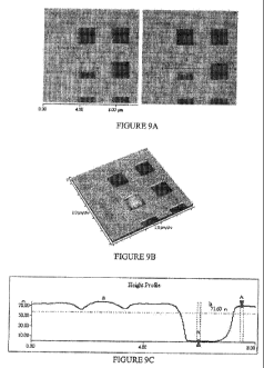
[0018] Figures 9A-9B are two- and three-dimensional AFM images, respectively,
of apertures after filling one of the apertures with an ink containing 1:10
weight ratio
of Mo(VI) oxide Bis(2,4-pentanedionate) to PCESQ and 4:1 volumetric ratio of
dimethylformamide to poly(ethyl)glycol using DPN printing. Figure 9C is a
height profile along "Line 1" in Figure 9A.
[0019] Figure 10 shows a series of AFM images of a MoSi microdot array before
and after three rounds of cleaning under the following conditions: 120 s in
piranha
(3:1 by volume H2SO4:H202) at 65 C, followed by sonication for 30 s at
20 watt/cm2, followed by sonication for 30 s at 4 watt/cm2, followed by 120 s
DI
rinse, followed by heating for 15 min at 100 C.
[0020] Figures I IA-11E show AFM images of a MoSi microdot array formed by
depositing an ink formulation containing Mo(VI) oxide Bis(2,4-pentanedionate)
and
PCESQ using DPN printing and photocuring by excimer laser irradiation.
Figure 12 describes phase shift mask ink formulation.
Figure 13 illustrates data for free standing PCESQ dot arrays on 6025 quartz
mask.
Figure 14 shows dot diameter size and optical image of free standing PCESQ
on 6025 quartz mask.
Figure 15 illustrates topographic AFM 2D and 3D images of MoSi film on
quartz substrates.
Figure 16 illustrates free standing MoSi Dot arrays on Si02 substrates.
Figure 17 shows dot diameter size and optical image of free standing PCESQ
on 6025 quartz mask.
Figure 18 illustrates free standing MoSi dot arrays on quartz mask.
6
CA 02766589 2011-12-22
WO 2011/002806 PCT/US2010/040470
Figure 19 illustrates varying deposition time of MoSi ink deposition in
square recessed features.
Figure 20 shows AFM and height contour plots of MoSi samples deposited
and cured in defect areas.
Figure 21 illustrates free standing MoSi dot arrays on Si02 substrate and
MoSi deposited in defect areas.
Figure 22 describes laser curing of MoSi films.
Figure 23 illustrates XPS spectra of laser cured MoSi films.
Figure 24 illustrates XPS spectra of uncured MoSi film.
Figure 25 illustrates XPS data for cured SiOx films by excimer laser.
Figure 26 illustrates excimer laser curing of free standing PCESQ dot
features.
Figure 27 illustrates excimer laser curing of free standing PCESQ dot
features.
Figure 28 illustrates gold coated AFM tip for ink deposition if difficulty
encountered in depositing certain Mo inks for some embodiments.
Figure 29 illustrates single and double deposition of Mo(V) PCSEQ ink in
MoSi mask defect areas.
Figure 30 illustrates deposition of Mo(V) PCSEQ ink on 6025 quartz mask.
Figure 31 illustrates deposition of Mo(V) PCSEQ in in MoSi mask defect
areas.
Figure 32 illustrates transmittance comparison between MoSi mask and
MoSi film.
DETAILED DESCRIPTION
[0021] INTRODUCTION/GENERAL
[0022] No admission is made that any reference cited herein is prior art. U.S.
Patent Number 6,635,311 to Mirkin et al. ("Methods Utilizing Scanning Probe
Microscope Tips And Products Therefor Or Produced Thereby"), which is hereby
7
CA 02766589 2011-12-22
WO 2011/002806 PCT/US2010/040470
incorporated by reference in its entirety, discloses a direct-write patterning
method
in which, for example, a sharp tip (e.g., a "pen") coated with a chemical
compound
or mixture (e.g., an "ink") is contacted with a substrate. With this method,
commercialized under Dip Pen NanolithographyTM printing ("DPN printing"),
arbitrary patterns may be fabricated with sub-20 nm resolution, 10 nm feature
alignment and a wide variety of inks, including but not limited to metal or
ceramic
precursors or nanoparticles can be used. The DPN printing nanotechnology
platform is commercialized by Nanolnk, Inc. (Skokie, IL). DPN , Dip Pen
NanolithographyTM, NanoInk are its trademarks.
[0023] In addition, U.S. Patent Application Number 10/689,547 to Crocker et
al,
which is hereby incorporated by reference in its entirety, and in particular
its Parts 6
and 7, teaches (i) the deposition of substantially optically transparent
materials, for
photomask repair application and (ii) the repair of advanced masks, such as
phase-
shift masks and NIL/SFIL molds, including the repair of voids in a transparent
substrate with sol-gel deposition, and the repair of partially transmitting
phase-
shifting layers, e.g., by deposition of molybdenum oxide or silicide
nanoparticle-
loaded sol-gel materials.
[0024] One embodiment described herein provides a method for repairing a
photomask comprising: providing a nanoscopic tip comprising an ink disposed on
the tip end, wherein the ink is formulated for curing at temperatures of about
100 C
to about 350 C; providing a photomask comprising region which needs to be
repaired; contacting the tip with the photomask in the region which needs to
be
repaired, wherein ink is transferred from the tip to the region; and forming a
cured
ink by (i) heating the ink at a temperature of about 100 C to about 350 C,
and/or (ii)
exposing the ink to electromagnetic radiation.
[0025] HEATING CURE EMBODIMENT
[0026] One embodiment comprises a heating cure step. In this embodiment, ink
cure is carried out either: (i) without a radiation exposure; or (ii) with a
supplemental
radiation exposure either before, during, or after the heating exposure. The
heating
step may be performed either on the entire photomask or on the localized
repair
region. Heat may be provided in any way that sufficiently raises the
temperature of
8
CA 02766589 2011-12-22
WO 2011/002806 PCT/US2010/040470
the ink to result in curing of the ink without damaging the photomask. For
example,
an oven or a hand-held heat gun may be used; or heating may be performed by
electron or ion bombardment. Other heating methods, such as resistive heating
within or around the photomask, can be readily used. Heating is performed at a
temperature of about 100 C to about 350 C, such as about 150 C to about 250 C,
such as about 250 C.
[0027] Figure IA shows an example of a photomask repair chip 100 that includes
a reading tip 102 for locating a defect to be repaired, a writing tip 104 for
depositing
an ink in the defect area, and a curing tip 106 for curing the deposited ink.
The
reading tip 102 can also be used for subtractive repair, including removing
excess
ink from the photomask. Optionally, the reading tip 102 is not used for
subtractive
repair, but the photomask repair chip comprises a fourth tip (not shown in
Figure
1 A) used for subtractive repair.
[0028] Figure 1 B shows the curing tip 106 of the repair chip 100. The curing
tip
106 includes a substrate handle 108 that supports a cantilever 110, at the end
of
which is a pyramidal tip 112. A resistive heater 114 is disposed on the bottom
surface of the cantilever 110. Alternatively, the resistive heater 114 can be
located
either on the top surface of the cantilever 110, or both top and bottom
surfaces.
Optionally, the resistive heater can be located only on or around the tip 112.
In an
embodiment, the heating cure step involves scanning the curing tip 106 over a
photomask region that is in need of repair. The temperature of the resistive
heater
114 can be controlled by varying the amount of current provided to the heater
114
through a wire 116 and/or by varying the resistivity of the heater 114, such
as by
changing the materials used in the heater 114. The curing conditions applied
to the
ink to be cured can be controlled by varying the scan rate of the curing tip
106
and/or by varying the distance between the photomask defect and the heater
114,
such as by varying the dimensions of the pyramidal tip 112.
[0029] Other heating mechanisms can be used to cure the ink. For example, a
pinpoint soldering gun which radiates heat at small distances, such as
distances less
than about 3 mm, can be brought into close proximity to the defect area, such
as
within a few microns above the defect area. The diameter of the tip of the
solder
9
CA 02766589 2011-12-22
WO 2011/002806 PCT/US2010/040470
gun can vary from about 1 mm to about 50 gm, such as about 100 m.
Alternatively, a resistive heating wire, such as a Nichrome-60 wire (or other
wires),
can be wrapped around a insulative tube, such as a ceramic tube, which can
then be
embedded in a concave shiny metallic apparatus to direct and reflect the
generated
heat from the wire onto the defect area. The localized heat source can also be
tipless
and have various geometries. For example, a microcantilever hotplate can be
used,
as described in J. Lee & W. King, "Microcantilever hotplates: Design,
fabrication,
and characterization," Sensors and Actuators A, 136 (2007) 291-298, which is
incorporated herein by reference in its entirety.
[0030] RADIATION CURE EMBODIMENT
[0031] Another embodiment comprises a radiation cure step. In this embodiment,
heating can also be performed to supplement the radiation cure, such as
before,
during, or after the heating cure step. Heating can also occur by the natural
action of
radiation cure.
[0032] The ink can cure upon exposure to UV, UV-visible, or visible light,
preferably at the wavelength used for lithographic exposure or photomask
inspection. Sources of UV light include but are not limited to lasers, such as
excimer lasers at a wavelength of 157 nm (F2), 193 nm (ArF) and 248 nm (KrF),
and
UV lamps, such as mercury lamps (184.9 nm), zinc lamps (213.9 nm), excimer
lamps at a wavelength of 126 nm (Ar), 146 nm (Kr), 172 nm (Xe), 193 nm (ArF),
222 nm (KrCI) and the like. Excimer lasers are commercialized by Lambda Physik
(Ft. Lauderdale, FL) and GAM lasers (Orlando, FL); excimer lamps are available
from Resonance (Ontario, CA), Radium Lampenwerk (Wipperfurth, Germany) and
Hoya Candeo (Japan), for example.
[0033] Irradiation conditions can be varied depending on the ink and
photomask.
Preferably, the irradiation conditions are below the damage threshold of the
photomask. For example, an ArF excimer laser can be pulsed at about 5
mJ/cm2/pulse to about 100 mJ/cm2/pulse, such as about 10 mJ/cm2/pulse to about
30
mJ/cm2/pulse, and more specifically about 13 mJ/cm2/pulse to about 20
mJ/cm2/pulse. The total dose can be determined by the pulse time, pulse
intensity,
and number of pulses. The number of pulses can be varied between 1 pulse to
CA 02766589 2011-12-22
WO 2011/002806 PCT/US2010/040470
60,000 puleses. The total dose can be about 50 mJ/cm2 to about 1,000 mJ/cm2,
such
as about 100 mJ/cm2 to about 700 mJ/cm2, and more specifically about 200
mJ/cm2
to about 400 mJ/cm2.
[0034] TIPS/CANTILEVERS/INSTRUMENTS
[0035] The tip is not particularly limited but can be a nanoscopic tip, such
as for
example a scanning probe microscopic tip, or specifically an atomic force
microscope (AFM) tip. The tip can be located at the end of a long cantilever
such as
used in an AFM. The tip can be longer than is customarily used for AFM
imaging,
having relative high aspect ratios. The tip can be made of Si3N4, Si, SiOX,
carbon
like diamond (CLD), diamond, doped tips with metal and semiconductor
materials,
etc. Arrays of tips can be used. The tips can be used with or without
supporting
cantilevers. The tip can have a tip radius of, for example, 100 nm or less, or
50 nm
or less, or 25 nm or less.
[0036] The tip can be coated with a polymer, such as polydimethysiloxane
(PDMS)-coated stamp tip, as described in U.S. Publication Number 2005/0255237
to Zhang et al. (Nanolnk), which is incorporated herein by reference in its
entirety.
The tip used for imaging the photomask can be different from the tip used for
depositing inks. For example, imaging can be performed using a bare Si3N4 tip,
while ink deposition is performed using a PDMS-coated stamp tip. The tip used
for
depositing inks may be cleaned prior to being coating with an ink. For
example, the
writing tip can be cleaned in RCA1 solution (H202: NH4OH: H2O 1:1:5 by volume)
for 10 min at 70 C. A third tip may comprise a resistive heating element,
such as
discussed with respect to in Figures lA-1B. A fourth tip may comprise a
subtractive
repair tip. Alternatively, the fourth tip is omitted and the imaging tip is
used for
subtractive repair.
[0037] The tip can be coated with a conductive material, such as a metal. For
example, a Si3N4 AFM tip can be first coated with 3 nm of titanium (Ti) and
can be
then coated with an additional 10 nm of gold (Au). The metal coating can be
thicker
or thinner, and different metals can be used such as Cr, W, etc, or
conductively-
doped AFM tips can be used. These conductive tips can be used, for example, to
reduce or eliminate the problem of electrostatic buildup when depositing high
Mo
11
CA 02766589 2011-12-22
WO 2011/002806 PCT/US2010/040470
content inks onto quartz or MoSi masks. Without wishing to be bound to any
particular theory, it is believed that the electrostatic charges are
dissipated or
neutralized when the conductive tip is brought into contact with the charged
mask.
The conductive tip can be modified with hydrophobic or hydrophilic molecules,
for
example via thiol functionalization of a gold-coated tip.
[0038] The tip can be dipped into a reservoir containing an ink. Prior to DPN
printing, the tip can be bled by repeatedly contacting it with a sacrificial
substrate,
until the ink deposition rate decreases and stabilizes. The deposition rate
and print
characteristics can be further controlled by varying such parameters as the
dwell
time, scan rate, scan mode (e.g., contact, non-contact, intermittent-contact
modes),
and spring constant of the AFM cantilever.
[0039] Instruments and accessories for microscale and nanoscale lithography
can
be obtained from Nanolnk (Chicago, IL), including the NSCRIPTORTM
instrumentation.
[0040] PHOTOMASK
[0041] A variety of photomasks can be used including those used for recognized
nodes such as the 65 nm node, the 45 mu node, and the like. Mask defects are
known in the art and include, for example, clear defects, which may be
repaired by
an additive repair process, and opaque defects, which may be repaired by a
subtractive repair process. Clear defects, which are missing or incomplete
features,
include, for example: pin-holes, broken or thinned lines, edge or notch
defects, and
corner defects. The defect region can be microscale or nanoscale.
[0042] Exemplary types of masks include the alternating aperture phase
shifting
photomasks (AAPSMs) and embedded attenuated phase shifting photomasks
(EAPSMs). AAPSMs, also called strong-shifters, can be fabricated by etching
180 -
phase-shifting windows in alternating clear areas of a quartz mask. EAPSMs,
also
called weak-shifters, can be fabricated by depositing a partially-transmitting
180 -
phase-shifting material, such as molybdenum silicide (MoSi), near clear
openings of
the photomask. Phase shift masks and methods of forming them are described in
U.S. Patent No. 7,011,910 to Shiota et al., which is incorporated herein by
reference
in its entirety.
12
CA 02766589 2011-12-22
WO 2011/002806 PCT/US2010/040470
[0043] The photomasks may be cleaned prior to being repaired. For example, the
photomask can be cleaned with piranha solution (a mixture of sulfuric acid and
hydrogen peroxide known in the art) for 60 seconds followed by 5.5 minutes in
RCAI solution (H202: NH4OH: H2O 1:1:5 by volume) at 120 C and by a deionized
water (DI) rinse.
[0044] INK COMPOSITION
[0045] The ink composition can be adapted for the cure, including for the
heating
cure embodiment or the radiation cure embodiment. The ink composition can be
further adapted to provide suitable optical properties including sufficient
transparency and sufficient refractive index to approximately match that of
the
photomask. Matching of the cured ink with the photomask can be achieved at or
around the wavelengths used for lithographic exposure, such that the
performance of
the repaired photomask is not substantially worse than that of a photomask
having
no defect. Color matching can be used as a facile indicator for larger-scale
repair
areas under optical microscopy inspection.
[0046] The ink composition can comprise a carrier solvent and a sol-gel
precursor
compound. Examples of carrier solvents include organic liquids including
alcohols
and alkanes. The alcohol may have the formula CõH(2r+2)0, wherein 4 <_n <_17.
Protic or aprotic solvents can be used. Examples include acetone, decanol,
dimethylformamide (DMF), and alpha terpinyl. The viscosity and evaporation
rate
of the ink composition can be adjusted by varying the ratio of solvent to sol-
gel
precursor. For example, the ink composition may contain solvent, relative to
the
precursors in the ink, at about 5 wt% to about 30 wt%, such as about 10 wt% to
25 wt%. In addition, the viscosity of the ink composition can be adjusted by
varying
the amount and size of the solvent molecule, such as by varying the length of
a long
carbon chain alcohol (e.g., CH3(CH2)nOH where n is greater than 5). Other
solvents
include diglyme [bis(2-methoxyethyl)] and poly(ethylene glycol) ["PEG"]. For
example, if PEG is used, its molecular weight may be about 200 g to about 600
g,
such as about 250 g. If DMF is present in the ink together with PEG, then a
volumetric ratio of DMF to PEG can be about 1:10 to about 10:1, such as about
1:5
to about 5:1. Where MoSi precursors are dissolved in decanol, the volumetric
ratio
13
CA 02766589 2011-12-22
WO 2011/002806 PCT/US2010/040470
of the MoSi precursors and decanol solution to DMF/PEG can be about 1:10 to
about 10:1, such as about 1:5 to about 5:1. Alternatively, acetone is
substituted for
DMF/ PEG. For example, the volumetric ratio of the MoSi precursors and decanol
solution to acetone is about 1:10 to about 10:1, such as about 1:5 to about
5:1.
[0047] The ink composition can contain at least one silicon dioxide precursor
that
is adapted to provide a silicon dioxide material upon cure. For example, the
ink
composition can include at least one photocurable silsesquioxane, such as
poly(2-
chloroethyl)silsesquioxane ("PCESQ"), which has an irradiation wavelength of
193 nm and results in a micro- or nanostructure primarily comprising silica.
Other
silicon dioxide precursors include but are not limited to: polyhedral
oligomeric
silsesquioxanes (POSS ) commercialized by Hybrid Plastics, silicon alkoxide,
and
tetraethoxyorthosilicate. The silsesquioxanes disclosed in U.S. Patent Number
5,853,808, which is incorporated herein by reference in its entirety, can also
be used.
[0048] PCESQ is suitable as a medium-temperature thermocurable ink, especially
when mixed with a fluoride ion catalyst. Catalysis with a fluoride ion
catalyst (e.g.,
tetrabutylammonium fluoride) lowers the silsesquioxane curing temperature,
such as
below 250 C, preferably below 200 C.
[0049] The ink composition can also contain a metal precursor that is adapted
to
provide a metal material upon cure, such as metal nanoparticles, metal salts,
metal
alkoxides, and metal acetylacetonates. Molybdenum nanoparticles includes
molybdenum silicide and molybdenum oxide nanoparticles or powders. Preferably,
the average diameter of the nanoparticles is far smaller than the typical
defect to be
repaired, for example, a few nanometers in diameter. The metal precursors also
include molybdenum salt or molybdenum acid salt. Examples include
molybdosilicic acid and salts thereof, molybdenum trioxide, heteropolyacids of
molybdenum, ammonium molybdate, and alkali metal or alkaline earth metal salts
of
the molybdate anion. For example, MoClx or MoOyClx is formed by adding MoO2
nanoparticles in a solution consisting of 1:1 ratio by volume of HCl and H202.
Other molybdenum compounds include: molybdenum(III) chloride (MOCl3),
molybdenum(V) chloride (MOC15), molybdenum(VI) dichloride dioxide (MoO2C12),
molybdenum(VI) tetrachloride oxide (MoOC14).
14
CA 02766589 2011-12-22
WO 2011/002806 PCT/US2010/040470
[0050] Metal alkoxides include alkoxides of the following metals: Sc, Ga, Y,
La,
Ln, Si, Ti, Ge, Zr, Hf, Nb, Ta, Mo, W, Fe, Co, Ni, Re, Pd. Examples of metal
alkoxides include: Ti(OC3H7-iso)4, Nb2(OCH3)10, Ta2(OCH3)10, [MoO(OCH3)4]2,
Re203(OCH3)6, Re4O6(OCH3)12, and Re406(OC3H7-iso)1o. For example,
molybdenum(V) ethoxide is used. The synthesis and isolation of molybdenum(V)
alkoxides and bimetallic alkoxides are described in "The solution thermolysis
approach to molybdenum(V) alkoxides: synthesis, solid state and solution
structures
of the bimetallic alkoxides of molybdenum(V) and niobium(V), tantalum(V) and
tungsten(VI),"A. Johansson et al., J. Chem. Soc., Dalton Trans. 2000, 387-398,
which is incorporated herein by reference in its entirety.
[0051] Metal acetylacetonates include acetylacetonates of the following
metals: Ti,
Fe, Ga, Zn, In, V, Nb, Ta, Hf, Mo, Mn, Cr, and Sn, as described in "Metal
Acetylacetonates as General Precursors for the Synthesis of Early
TransitionMetal
Oxide Nanomaterials," A. Willis et al., J. Nanomaterials 2007, 1-7 (Article ID
14858), which is incorporated herein by reference in its entirety. For
example,
molybdenum(VI) oxide Bis(2,4-pentanedionate) is used.
[0052] The optical properties of the ink can be tuned by varying the
concentration
of ink components, such as by varying the ratio of metal precursor to silicon
dioxide
precursor within the ink. For example, the atomic ratio of Mo to Si in the ink
can be
equal to about 1:50 to about 50:1, such as about 1:25 to about 25:1, for
example
about 1:10 to about 10:1, and more specifically about 1:5 to about 5:1.
Control of
the atomic ratio of Mo to Si can be performed by varying either the volumetric
or
weight ratios of molybdenum precursors to silicon dioxide precursors. For
example,
the volumetric ratio of the molybdenum precursor to the silicon dioxide
precursor is
in the range of about 1:50 to about 50:1, such as about 1:25 to about 25:1,
for
example about 1:10 to about 10:1, and more specifically about 1:5 to about
5:1. In
an alternative embodiment, the weight ratio of the molybdenum precursor to the
silicon dioxide precursor is in the range of about 1:50 to about 50:1, such as
about
1:25 to about 25:1, for example about 1:10 to about 10:1, and more
specifically
about 1:5 to about 5:1. For example, a sol-gel ink formulation includes PCESQ
and
a molybdenum precursor made from at least one of Mo(V) ethoxide or
molybdenum(VI) oxide Bis(2,4-pentanedionate).
CA 02766589 2011-12-22
WO 2011/002806 PCT/US2010/040470
[0053] The ink composition can be adapted to have the ability to coat a tip,
and
then be deposited from the tip to a substrate.
[0054] PROPERTIES OF REPAIRED MASK
[0055] An advantage of the repaired mask is that the cured ink adheres well to
the
mask and survives washing steps commonly used in the semiconductor industry.
For example, the cured ink can survive repeated washing steps in piranha
solution,
RCAI solution, RCA2 solution, and deionized water. Preferably, the thermal
expansion coefficient of the cured ink is approximately equal to that of the
photomask, thereby allowing the cured ink to expand and contract with the
surrounding photomask during thermal cycling without cracking or pealing off
from
the photomask.
[0056] A further advantage of the repaired mask is that the optical properties
of the
cured ink approximately match those of an undamaged mask. For example, the
optical properties of Mo-Si based EAPSM films are set forth in H. Kobayashi et
al.,
"Photomask blanks quality and functionality improvement challenges for the 130-
nm node and beyond," Proc. SPIE, Vol. 4349, p. 164-169, 17th European
Conference on Mask Technology for Integrated Circuits and Microcomponents,
Uwe F. Behringer; Ed. (2001), particularly Figure 3, which is incorporated
herein by
reference in its entirety. Transmittance of the cured ink can be, for example,
about
5% to about 25% of incident light. It can be, for example, 5% to 10%, or 10%
to
20% for high transmittance masks. The transmittance of the cured ink is tuned
by
varying, for example, the refractive index (n), the extinction coefficient
(k), and the
thickness (t) of the cured ink. For incident light with a wavelength of 193
nm, the
refractive index (n) of the cured ink can equal about 1.00 to about 2.6, such
as about
1.30 to about 2.45, for example about 2.0 to about 2.4, and more specifically
about
1.55 to about 2.03. For incident light with a wavelength of 193 nm, the
extinction
coefficient (k) of the cured ink can equal about 0.03 to about 0.90, such as
about
0.20 to about 0.75, for example about 0.3 to about 0.6, and more specifically
about
0.38 to about 0.63. The thickness (t) of the cured ink can vary from a few
nanometers to several hundred microns or more, but is preferably about 10 nm
to
16
CA 02766589 2011-12-22
WO 2011/002806 PCT/US2010/040470
1,000 nm, such as about 30 nm to about 650 nm, and more specifically about 50
nm
to about 100 nm.
[0057] The invention is further described with use of the following non-
limiting
examples, which include a description of the figures.
EXAMPLE 1
[0058] Preparation, DPN Printing and Thermal Curing of PCESQ Compositions
[0059] A commercially-available alternating-aperture photomask (AAPSM) was
cleaned with piranha solution (a mixture of sulfuric acid and hydrogen
peroxide
known in the art) for 60 s followed by 5.5 min in RCA1 solution (H202: NH4OH:
H2O 1:1:5 by volume) at 120 C and by a deionized water (DI) rinse. A
commercially-available silicon nitride tip was cleaned in RCA1 for 10 min at
70 C.
A sol-gel mixture was prepared by mixing poly(2-chloroethyl)silsesquioxane
("PCESQ") and decanol (density 0.8297 g/ml) in a 10:1 ratio by volume. The tip
was coated by being immersed in the sol-gel mixture for 15 s.
[0060] A portion of the mask was imaged by AFM, and a region comprising three
apertures at least 200-nm in depth was located. Figure 2A shows an AFM image
of
the AAPSM after the middle aperture was repaired via DPN printing by using a
scanning probe microscopy instrument NSCRIPTORTM (Nanolnk, Skokie IL) under
ambient conditions (22 C to 24 C and 20% to 40% relative humidity). After
deposition, the substrate was heated for 16 hr in an oven at 120 C followed by
5 min
of heating with a hand-held heat gun (- 300 C). Figure 2B shows a height
profile
line-scan along "Line 1" in Figure 2A showing that the middle aperture was
substantially filled.
[0061] The dwell time of the tip over the defective region can be varied.
Optionally, subtractive repair can be performed to remove excess cured
material.
[0062] Cured Si02 structures formed by the above-described method exhibited
remarkable robustness to cleaning with piranha solution, RCA1 solution, and
rinsing
with DI water on quartz, glass, and silicon oxide. For example, the change in
average height and width of the microdots after repeated cleaning was less
than
about 3% (within the margin of error). Thus, the cured Si02 structures are
chemically and mechanically stable.
17
CA 02766589 2011-12-22
WO 2011/002806 PCT/US2010/040470
EXAMPLE 2
Photocuring of PCESQ Compositions
[0063] An array of 33 microdots was formed by depositing poly(2-
chloroethyl)silsesquioxane ("PCESQ") on a quartz substrate using DPN printing
as
described in Example 1. Prior to photocuring, the uncured sol-gel structures
were
too soft to be imaged by AFM but could be easily observed via optical
microscopy.
These structures were then heated using deep UV radiation with a commercial
ArF
excimer having a 193 nm wavelength. Irradiation was performed using a pulse
does
of 13.3 mJ/cm2/pulse and a total dose of 250 J/cm2.
EXAMPLE 3
Optical Properties of MoSi Compositions
[0064] A 66 rim-thick thin film of MoSi was deposited by physical vapor
deposition (PVD). Ellipsometry measurements were performed on the MoSi film to
determine the film's refractive index (n) and extinction coefficient (k) as a
function
of wavelength. Figure 3A is a plot of n and k versus wavelength for the PVD-
deposited film. For a wavelength of 193 nm, n = 2.45 and 0.38 <_0.55.
Formulation:
[0065] Four different ink formulations were made (labeled A, B, C, D), and
their
optical properties were tested in three rounds of testing. In Round 1,
formulation
A(l, 2) contained 0.002 g of MoO2 nanoparticles and 1 L of PSESQ. Formulation
B(3) contained a 1:4 volumetric ratio of MoOXC1y to PSESQ. Formulation C(4,5)
contained 1:7 and 1:15 volumetric ratios of molybdenum(VI) oxide Bis(2,4-
pentanedionate) to PCESQ, respectively. Formulation D(6,7) contained 1:200 and
1:400 volumetric ratios of Mo(OCH2CH3)5 to PCESQ, respectively. Table 1 shows
the ellipsometry data for Round I at a wavelength of 193 nm.
18
CA 02766589 2011-12-22
WO 2011/002806 PCT/US2010/040470
[0066] TABLE 1
Round I
Ink formulation n k
A(1) 1.35 0.07
A(2) 1.15 0.12
B(3) 1.00 0.07
C(4) 1.60 0.05
C(5) 1.85 0.08
D(6) 1.35 N/A
D(7) 1.42 0.03
[0067] In Round II, formulation D(1, 2, 3, 4) contained Mo(OCH2CH3)5 and
PCESQ in the following volumetric ratios: 1:30, 1:60, 1:90, and 1:120,
respectively.
Formulation C(5, 6, 7) contained molybdenum(VI) oxide Bis(2,4-pentanedionate)
and PCESQ in the following volumetric ratios: 1:4, 1:8, and 1:12,
respectively.
Table 2 shows the ellipsometry data for Round II at a wavelength of 193 nm.
[0068] TABLE 2
Round II
Ink formulation n k
D(1) 1.46 0.018
D(2) 1.03 0.032
D(3) 1.19 0.035
D(4) 1.00 0.040
C(5) 1.55 0.195
C(6) 1.55 0.155
C(7) 1.50 0.046
[0069] In Round III, formulation C(1, 2, 3, 4) contained molybdenum(VI) oxide
Bis(2,4-pentanedionate) and PCESQ in the following volumetric ratios: 1:1,
5:1,
10:1, and 20:1, respectively. Formulation D(5, 6, 7) contained Mo(OCH2CH3)5
and
PCESQ in the following volumetric ratios: 2.5:1, 1:1 + decanol, and 1.5:1
respectively. Table 3 contains the ellipsometry data for Round III at a
wavelength of
193 nm.
19
CA 02766589 2011-12-22
WO 2011/002806 PCT/US2010/040470
[0070] TABLE 3
Round III
Ink formulation n k
C(1) 1.30 0.19
C(2) 1.15 0.22
C(3) 1.65 0.89
C(4) 1.65 0.75
D(5) 1.29 0.35
D(6) 1.34 0.23
D(7) 2.03 0.63
[0071] Figures 3B-3D are plots of measured n and k versus wavelength for
selected inks from Rounds I, II, and III, respectively. Specifically, Figure
3B is a
plot of n and k versus wavelength for Round I, Formulation C(5). Figure 3C is
a
plot of n and k versus wavelength for Round II, Formulation C(5). Figure 3D is
a
plot of n and k versus wavelength for Round III, Formulation D(7). Notably,
the n
and k curves in Figures 3C-3D follow the same general trends as the CVD-
deposited
MoSi film in Figure 3A. Final values for n and k are shown for 193 nm
wavelengths.
EXAMPLE 4
Preparation of Mo(V) Ethoxide and PCESQ Compositions
[0072] Eight ink formulations were prepared by adding decanol (density
0.8297 g/ml) to an ethanolic stock solution of Mo(V) ethoxide and leaving the
solution open in an ependorf tube for 24 to 72 hours until the ethanol
evaporated.
After evaporation, poly(2-chloroethyl)silsesquioxane ("PCESQ") was added to
solution. The relative quantities of each component are shown in Table 4 for
each
ink formulation. The weight percent of decanol in each ink formulation was
measured relative to the total weight of Mo(V) ethoxide and PCESQ.
CA 02766589 2011-12-22
WO 2011/002806 PCT/US2010/040470
[00731 TABLE 4
Ink Mo(V) ethoxide PCESQ Decanol
(mg) (mg) (wt. %)
1 15 60 19
2 8 24 13
3 8 24 18
4 9.8 19.4 16
12.3 13.5 17
6 30.2 17.3 26
7 28.5 14.4 22
8 15.4 62.2 22
EXAMPLE 5
Preparation of MoSi Thin Films from Mo(V) Ethoxide and PCESQ Compositions
[00741 An ink formulation was prepared by adding decanol (density 0.8297 g/ml)
to an ethanolic stock solution of Mo(V) ethoxide and leaving the mixture open
in an
ependorf tube for 24 to 72 hours until the ethanol evaporated. After
evaporation,
poly(2-chloroethyl)silsesquioxane ("PCESQ") was added to the solution. The
ratio
of Mo(V) ethoxide to PCESQ was 1:10 by weight. The amount of decanol was
20 wt.% of the total weight of Mo(V) ethoxide and PCESQ. A silicon dioxide
substrate (1 inch square) was treated with HF prior to being spin coated with
400 gL
of the ink formulation for 5 s at 500 rpm, followed by 30 s at 1500 rpm. The
film
was heated for 60 min at about 300 C. The result was a thin film of MoSi
having a
thickness of 240 nm. Thicknesses of about 100 nm can be obtained, for example,
by
depositing less than 400 L of ink, such as about 50 L to about 300 L.
Ellipsometry measurements were performed on the cured ink, and curve fitting
was
performed to obtain the film thickness and n and k values. Figure 4 shows that
for a
spectrum range of 1.5 eV to 6.5 eV and a film thickness of 240 nm, the values
for n
and k at 190 nm wavelength were 1.7 and 0.2, respectively.
21
CA 02766589 2011-12-22
WO 2011/002806 PCT/US2010/040470
EXAMPLE 6
DPN Printing of Mo(V) Ethoxide and PCESQ Compositions
[0075] An ink formulation was prepared by adding decanol (density 0.8297 g/ml)
to an ethanolic stock solution of Mo(V) ethoxide and leaving the solution open
in an
ependorf tube for 24 to 72 hours until the ethanol evaporated. After
evaporation,
poly(2-chloroethyl)silsesquioxane ("PCESQ") was added to solution. The ratio
of
Mo(V) ethoxide to PCESQ was 1:5 by volume. The amount of decanol was
20 wt.% of the total weight of Mo(V) ethoxide and PCESQ. The ink formulation
was deposited from an AFM tip on a Si02 substrate using DPN printing and was
thermally cured at 200 C for 1 hr. Figure 5 shows an AFM image of a 3X3 array
of
cured ink microdots formed by holding the tip over each deposited region for
20 s
(bottom row), 40 s (middle row), and 60 s (top row).
EXAMPLE 7
Mo(V) Ethoxide and PCESQ Compositions with Tetrabutylammonium Fluoride
Catalyst
[0076] A first ink formulation was prepared by adding decanol (density
0.8297 g/ml) to an ethanolic stock solution of Mo(V) ethoxide and leaving the
solution open in an ependorf tube for 24 to 72 hours until the ethanol
evaporated.
After evaporation, poly(2-chloroethyl)silsesquioxane ("PCESQ") was added to
solution. The ratio of Mo(V) ethoxide to PCESQ was 1:4 by weight. The amount
of
decanol was 20 wt.% of the total weight of Mo(V) ethoxide and PCESQ. The first
ink formulation was deposited by spin coating onto a HF-treated silicon
substrate.
The film was heated at 200 C for 1 hr. X-ray photoelectron spectroscopy (XPS)
was performed on the film. Figure 6A is an XPS spectrum of the cured first ink
and
shows the presence of a carbon peak at around 290 eV.
[0077] A second ink formulation was prepared according to the method and
compositions used in the first ink formulation, except that 6 wt%
tetrabutylammonium fluoride catalyst was added to the final mixture. The
amount
of catalyst added was 6% of the total weight of the MoSi solution. The second
ink
formulation was deposited by spin coating onto a HF-treated silicon substrate.
The
film was heated at 200 C for 1 hr. X-ray photoelectron spectroscopy (XPS) was
22
CA 02766589 2011-12-22
WO 2011/002806 PCT/US2010/040470
performed on the film. Figure 6B is an XPS spectrum of the cured second ink
and
shows a much smaller peak at around 290 eV as compared with Figure 6A,
indicating a suppression of the carbon peak due to the presence of the
catalyst.
Figure 6C shows an XPS spectrum of the second ink heated at 350 C. A small
carbon peak is visible and is attributed to carbon contamination during sample
handling. These results show that the tetrabutylammonium fluoride catalyst
decreased the curing temperature of the ink formulation, as evidenced by the
relatively smaller carbon peak in Figure 6B.
[0078] A third ink formulation was prepared by adding decanol (density 0.8297
g/ml) to an ethanolic stock solution of Mo(V) ethoxide and leaving the
solution open
in an ependorf tube for 24 to 72 hours until the ethanol evaporated. After
evaporation, poly(2-chloroethyl)silsesquioxane ("PCESQ") was added to
solution.
The ratio of Mo(V) ethoxide to PCESQ was 1:4 by weight. The amount of decanol
was 20 wt.% of the total weight of Mo(V) ethoxide and PCESQ. The ratio of
Mo(V) ethoxide to PCESQ was 1:4 by volume. The amount of decanol was 17 gL
(20 wt.% of the total weight of Mo(V) ethoxide and PCESQ). Then, 3 wt%
tetrabutylammonium fluoride catalyst was added to the third ink formulation.
The
amount of catalyst added was 3% of the total weight of the Mo(V)Si solution.
Figures 7A-7B show optical microscope images of an array of defects in a
photomask before (Figure 7A) and after (Figure 7B) the third ink formulation
was
deposited onto a Si02 surface using DPN printing. The ink in Figure 7B was
not
cured. The tip holding time was 10 s per defect.
EXAMPLE 8
Preparation of Mo(VI) oxide Bis(2,4-pentanedionate) and PCESQ Compositions
[00791 Mo(VI) oxide Bis(2,4-pentanedionate) was dissolved in 500 .iL of
ethanol
and reduced for several weeks at room temperature. Reduction was observed to
begin after one week and reached completion after four weeks. The color of the
solution changed from a yellow color to dark blue upon reduction. The solution
was
then added together with poly(2-chloroethyl)silsesquioxane ("PCESQ") to
decanol
(density 0.8297 g/ml). The relative quantities of each component are shown in
Table 5 for each ink formulation. In order to determine the weight amount of
23
CA 02766589 2011-12-22
WO 2011/002806 PCT/US2010/040470
Mo(VI), the solvent of a known amount (20 L) of the ethanolic Mo(VI) solution
was evaporated. The determined weight was used as the standard weight for a
20 L Mo(VI) sample. Appropriate amounts of PCESQ were added depending on
the desired ratio, for example the 20 L solution yielded a 0.001 g solid
after ethanol
evaporation. Thus, to obtain a 0.01 g of Mo(VI), 200 L of solution was used.
The
weight percent of decanol in each ink formulation was measured relative to the
total
weight of Mo(VI) oxide Bis(2,4-pentanedionate) and PCESQ.
[0080] TABLE 5
Mo(VI) oxide Bis(2,4-
Ink pentanedionate):PCESQ Decanol
(Volumetric ratio) ( % of total)
1 1:64 20
2 1:20 20
3 1:10 20
4 1:4 20
1:1 20
6 2:1 20
7 4:1 20
[0081] Figures 8A-8B show AFM images of an array of defects before (Figure
8A) and after (Figure 8B) defect filling was performed with Ink Formulation 3
(1:10
Mo(VI) oxide Bis(2,4-pentanedionate):PCESQ by volume) using DPN printing by
slowly scanning the coated AFM tip across the defect area. The samples were
cured
at 200 C for 1 hr. Each defect feature has a length and width of about 2 m
and
0.6 m, respectively.
EXAMPLE 9
DPN Printing of Mo(V) Ethoxide and PCESQ Compositions
[0082] An ink formulation was prepared according to the method described in
Example 5. The ratio of Mo(V) ethoxide to PCESQ was 1:10 by weight. The
amount of decanol was 20 wt.% of the total weight of Mo(V) ethoxide and PCESQ.
Then, a 4:1 ratio by volume of DMF and PEG (molecular weight 250 g) was added
to the first ink formulation. The ratio of the Mo(V)Si and the DMF:PEG
solutions
24
CA 02766589 2011-12-22
WO 2011/002806 PCT/US2010/040470
was 1:5. The ink formulation was deposited from an AFM tip into a 2 m-wide,
70 nm-deep aperture of a quartz photomask using DPN printing. The deposited
ink was cured at 200 C for 1 hr. Figures 9A-9B show two- and three-dimensional
AFM images, respectively, of the aperture that is substantially filled with
the cured
ink. Figure 9C shows a height profile line-scan along "Line 1" in Figure 9B,
with
locations "a" and "b" representing the repaired aperture and an adjacent
unfilled
aperture, respectively.
EXAMPLE 10
Stability of Cured MoSi Inks
[0083] An array of MoSi microdots was formed by depositing an ink formulation
containing Mo(V)Si 1:10 ratio in 20 wt% decanal on a Si02 substrate using DPN
printing and heating the array in an oven at 225 C for 60 min. After curing,
the
array was subjected to three rounds of cleaning under the following
conditions:
120 s in piranha (3:1 by volume H2SO4:H202) at 65 C, followed by sonication
for
30 s at 20 watt/cm2, followed by sonication for 30 s at 4 watt/cm2, followed
by 120 s
DI rinse, followed by heating for 15 min at 100 C. Figure 10 shows a series of
AFM images of the array before and after each round of cleaning. The average
height (83 nm) and width (1.7 m) of the MoSi microdots before and after the
three
rounds was within 3% (within the margin of error) and thus was not appreciably
affected by the aggressive cleaning regimen. Similar results (not shown) were
obtained for MoSi microdots having an average height and width of 14.5 nm and
600 nm, respectively.
EXAMPLE 11
Photocuring of Mo(V) Ethoxide and PCESQ Compositions
[0084] An array of MoSi microdots was formed by depositing an ink formulation
containing Mo(V) ethoxide and PCESQ on Si02 and quatz mask substrates using
DPN printing and photocuring by excimer laser irradiation. The wavelength of
the
excimer laser was 193 nm under various irradiation conditions: Energy density
was
varied from 5, 25, 50, 75 and 100 mJ/cm2. Repetition rate was varied from 20
and
50 Hz. Number of pulses was varied from 100, 4000, 6000, 7600, 12000 and
60000.
Process time was varied from 5, 80, 120, 200, 240, 300, 390 and 1200 sec.
CA 02766589 2011-12-22
WO 2011/002806 PCT/US2010/040470
[0085] Figures 11A-11 E show AFM images and corresponding line scans of the
resultant 2x2 MoSi microdot arrays. In Figure I IA, the irradiation conditions
were:
mJ/cm2, 50 Hz, 60000 pulses, 1200s, 10 sec. In Figure 11 B, the irradiation
conditions were: 25 mJ/cm2, 50 Hz, 12000 pulses, 240s, 10 sec. In Figure 11 C,
the
irradiation conditions were: 50 mJ/cm2, 20 Hz, 6000 pulses, 300s, 10 sec. In
Figure
11 D, the irradiation conditions were: 75 mJ/cm2, 20 Hz, 4000 pulses, 200s, 10
sec.
In Figure 11 E, the irradiation conditions were: 25 mJ/cm2, 50 Hz, 12000
pulses,
240s, 1 sec.
[0086] Additional working examples are shown in Figures 12-32.
[0087] In another example, MoSi thin film deposition on silicon and quartz
substrates was carried out. Spin coating was used to prepare films with about
75 nm
thickness. The MoSi film on the quartz material resembled in color an
evaporated
thin MoSi film. The solvent system DMF-PEG was replaced with acetone.
Thickness and optical properties were measured by ellipsometry.
Ratio 1:2 1:1 2:1
Thickness 80 79 97
Refractive index 1.72 1.72 1.82
n
k 0.5 0.66 0.83
[0088] In another example for making MoSi films on quartz masks inexpensively,
MoSi thin films were made on quartz masks. 200 microliters of MoSi ink (1:10
ratio) were deposited onto a one inch square piece taken from a quartz mask.
The
spinning was carried out with spin coater for 5 sec at 500 rpm followed by 30
sec at
1500 rpm, curing of the piece between 250 and 350 C for an hour, which formed
a
nice smooth film. For use of 400 microliters, a 300 nm film was formed. A
target
thickness is 100 nm.
26
CA 02766589 2011-12-22
WO 2011/002806 PCT/US2010/040470
[0089] Ellipsometry Measurements:
[0090] Ellipsometry is a non-destructive optical technique used for measuring
thin
layer thickness. It has useful capabilities for thin film characterization
such as
thickness, optical properties as well as band gap of the material. This
technique is
based on the measurement of the change in light polarization upon reflection
from a
sample surface; ellipsometry derives thin films thickness and optical
properties
(refractive index "n" and absorption coefficient "k") with extreme accuracy.
The
spectroscopic capability allows for simultaneous determination of multiple
parameters: for example multi-layer thickness and composition of thin film
stacks.
The ellipsometric raw data collected by the UVISEL a Phase Modulated
Spectroscopic Ellipsometry (Jobin Yvon, Inc.) are converted into traditional
ellipsometric data. The material properties such as thickness and optical
constants n
and k are deduced by fitting the experimental data to theoretical models build
with
the ellipsometry analysis software, Delta Psi 2. Validity and robustness of
the
model is double checked for every measured point by using a minimization
algorithm based on Chi Square (X2) method and by calculating a correlation
matrix.
The optical properties of the MoSi film shown in the figures represented
herein are
presented by blue line for n and red line for k at different wavelength from
190 to
820 nm.
[0091] The following experimental conditions were used for the MoSi thin
films:
^ Spectral range of measurement 190 to 820 nm
^ [0092] Spot size: 1 mm diameter.
^ [0093] Integration time: 200ms
27