Note: Descriptions are shown in the official language in which they were submitted.
CA 02766726 2014-12-02
UNITED STATES UTILITY PATENT APPLICATION
for
TWO LEVEL LIGHTING BA.LLAST
Inventors: Nitin Kumar, Shashank Bakre, and Thomas J.
Schalton
TECHNICAL FIELD
[0001] The present invention relates to lighting, and more specifically, to
electronic ballasts for
powering lamps.
BACKGROUND
[0002] Multiple level lighting systems allow a user to set the level of light
the user desires to
receive from the lamp or lamps within the lighting system. For example, a two
level lighting
systems allows the user to select between two different levels of light: full
on, such that the lamp
or lamps in the lighting system is/are at their maximum output setting, and
half on, such that the
lamp or lamps in the lighting system is/are at half of their maximum output
setting. As a result,
multiple level lighting systems are typically used in overhead lighting
applications, to give the
user a choice between levels of light.
[0003] A typical implementation of a two level lighting system includes two
power switches and
two ballasts. Each power switch in the lighting system controls only one of
the ballasts in the
lighting system. Turning on both of the switches at the same time powers both
ballasts, thus
producing full light output from the lighting system. Turning on only one of
the switches applies
power to only one of the ballasts in the lighting system and thus results in a
reduced light level
and a corresponding reduction in power consumed.
SUMMARY
[0004] The conventional two level lighting system described above suffers from
a variety of
deficiencies, most notably in economy. It is more economical to use only a
single ballast instead
of the two ballasts typically found in the conventional two level lighting
system. One
CA 02766726 2014-12-02
implementation of a two level lighting system using only a single ballast
requires two switches
and two lamp sets. Alternatively, a two level lighting system using only a
single ballast may
include two lamp sets and two controllers within the ballast, where each
controller controls a lamp
set. In order to shut off one lamp set, the supply voltage to the controller
corresponding to that
lamp set is pulled down (e.g., grounded) so that the controller is disabled.
However, this
implementation is not energy efficient. In addition to continuing to require
two lamp sets, even
though one of the two controllers is disabled, the supply voltage for that
controller is still being
pulled into the ballast from the power supply.
[0004a] In an aspect of the invention, there is provided a ballast comprising:
a self-oscillating
inverter circuit having an inverter input to receive direct current (DC)
voltage and an inverter
output to selectively provide an alternating current (AC) lamp current to
energize one or more
lamps, the self-oscillating inverter circuit comprising: a switching circuit,
wherein the switching
circuit operates at a switching frequency; a feedback transformer connected to
the inverter output
to drive the switching circuit as a function of the lamp current at the
inverter output; and an
impedance component connected in parallel with the feedback transformer
between the inverter
input and the feedback transformer; the switching circuit operating such that,
when the impedance
component is enabled, the switching circuit operates at a switching frequency
in a first frequency
range and a first lamp current is provided to the one or more lamps; the
switching circuit operating
such that, when the impedance component is disabled, the switching circuit
operates at a switching
frequency in a second frequency range and a second lamp current is provided to
the one or more
lamps, wherein the first frequency range is lower than the second frequency
range and the first
lamp current is greater than the second lamp current; and a control circuit
connected to the
impedance component of the inverter circuit, wherein the control circuit
selectively operates the
impedance component between a first state, in which the impedance component is
enabled, and a
second state, in which the impedance component is disabled; wherein the
control circuit comprises
a first transistor and a second transistor, wherein the first transistor is
selectively connected and
disconnected to an AC power supply, and the second transistor is connected to
the first transistor
and to the impedance component, wherein when the first transistor is connected
to the AC power
supply, the first transistor is conductive, the second transistor is
nonconductive, and the impedance
component is disabled, and when the first transistor is disconnected from the
AC power supply,
the first transistor is nonconductive, the second transistor is conductive,
and the impedance
component is enabled.
2
CA 02766726 2014-12-02
[0004b] In another aspect of the invention, there is provided a ballast
comprising: a self-
oscillating inverter circuit having an inverter input to receive direct
current (DC) voltage and an
inverter output to selectively provide an alternating current (AC) lamp
current to energize one or
more lamps, wherein the self-oscillating inverter circuit: operates in a first
state having a switching
frequency in a first frequency range, wherein the self-oscillating inverter
circuit provides a first
lamp current to the one or more lamps; and operates in a second state having
at a switching
frequency in a second frequency range, wherein the self-oscillating inverter
circuit provides a
second lamp current to the one or more lamps, wherein the first frequency
range is lower than the
second frequency range and the first lamp current is greater than the second
lamp current; and a
control circuit connected to the inverter circuit to control an impedance of
the inverter circuit to
selectively operate the inverter circuit between the first state and the
second state; wherein the
control circuit comprises a first transistor and a second transistor, wherein
the first transistor is
selectively connected and disconnected to an AC power supply, and the second
transistor is
connected to the first transistor and to an impedance component of the self-
oscillating inverter
circuit, wherein when the first transistor is connected to the AC power
supply, the first transistor is
conductive, the second transistor is nonconductive, and the impedance
component is disabled, and
when the first transistor is disconnected from the AC power supply, the first
transistor is
nonconductive, the second transistor is conductive, and the impedance
component is enabled.
[0005] Embodiments disclosed herein also provide a multiple level lighting
system using a single
ballast that overcomes the deficiencies of the conventional two level lighting
systems. In
particular, embodiments are directed to a ballast having a self-oscillating
inverter circuit and a
control circuit. The control circuit operates a single lamp set between a
first lighting level and a
second lighting level. The first lighting level provides a greater amount of
lumens than the second
lighting level. In some embodiments, the self-oscillating inverter circuit has
an inverter input to
receive direct current (DC) voltage and an inverter output to selectively
provide an alternating
current (AC) lamp current to energize the lamp set. The control circuit
adjusts an amount of
impedance provided at the input of the inverter circuit. The control circuit
makes this adjustment
such that, when a first level (e.g., high level) of impedance is provided at
the input of the inverter
circuit, the lamp set operates at the first lighting level, and when a second
level (e.g., low level) of
impedance is provided at the input of the inverter circuit, the lamp set
operates at the second
lighting level.
2a
CA 02766726 2014-12-02
[0006] In some embodiments, the inverter circuit may include a switching
circuit to operate at a
switching frequency and a feedback transformer connected to the inverter
output to drive the
switching circuit as a function of the lamp current at the inverter output. An
impedance
component, such as a capacitor, is connected in parallel with the feedback
transformer between the
inverter input and the feedback transformer. The control circuit is connected
to the impedance
component to selectively operate the impedance component between a first state
and a second
state. In the first state, the impedance component is enabled. In the second
state, the impedance
component is disabled. When the impedance component is enabled, the switching
circuit operates
at a switching frequency in a first frequency range, and a first lamp current
is provided to the lamp
set. When the impedance component is disabled, the switching circuit
2b
CA 02766726 2014-12-02
operates at a switching frequency in a second frequency range, and a second
lamp current is
provided to the lamp set. Accordingly, the first frequency range is lower than
the second
frequency range, and the first lamp current is greater than the second lamp
current. Thus, the
lamp set operates at the first lighting level, providing more lumens, when the
impedance
component is enabled, and the lamp set operates at the second lighting level,
providing less
lumens, when the impedance component is disabled.
[0007] In an embodiment, there is provided a ballast. The ballast includes: a
self-oscillating
inverter circuit having an inverter input to receive direct current (DC)
voltage and an inverter
output to selectively provide an alternating current (AC) lamp current to
energize one or more
lamps. The self-oscillating inverter circuit includes: a switching circuit,
wherein the switching=
circuit operates at a switching frequency; a feedback transformer connected to
the inverter output
to drive the switching circuit as a function of the lamp current at the
inverter output; and an
impedance component connected in parallel with the feedback transformer
between the inverter
input and the feedback transformer. The switching circuit operates such that,
when the
impedance component is enabled, the switching circuit operates at a switching
frequency in a
first frequency range and a first lamp current is provided to the one or more
lamps; and when the
impedance component is disabled, the switching circuit operates at a switching
frequency in a
second frequency range and a second lamp current is provided to the one or
more lamps, wherein
the first frequency range is lower than the second frequency range and the
first lamp current is
greater than the second lamp current. The ballast also includes a control
circuit connected to the
impedance component of the inverter circuit, wherein the control circuit
selectively operates the
impedance component between a first state, in which the impedance component is
enabled, and a
second state, in which the impedance component is disabled.
[0008] In a related embodiment, the impedance component may be a capacitor. In
another
related embodiment, the switching circuit may be a half-bridge resonant
inverter having a first
switching component and a second switching component. In a further related
embodiment, the
feedback transformer may include a primary winding, a first secondary winding
to drive the first
switching component, and a second secondary winding to drive the second
switching component,
and the impedance component may be connected in parallel with primary winding
between the
inverter input and the primary winding.
3
CA 02766726 2014-12-02
[0009] In another related embodiment, the first frequency range may be 195 to
205 kHz, and the
second frequency range may be 215 to 220 kHz. In yet another related
embodiment, the ballast
may further include: an electromagnetic interference filter configured to
receive alternating
current (AC) voltage from a power source; a rectifier connected to the
electromagnetic
interference filter to convert the alternating current (AC) voltage to direct
current (DC) voltage; a
power factor correction circuit connected to the rectifier to produce a DC
voltage output; and a
DC voltage bus connected to the power factor correction circuit to receive the
DC voltage output
from the power factor correction circuit, the inverter input may be connected
to the DC voltage
bus to receive the DC voltage. In a further related embodiment, the control
circuit may have a
first control circuit input and a second control circuit, the first control
circuit input may be
selectively connected and disconnected to an AC power supply via a switch, and
the second
control circuit input may be connected between the rectifier and the power
factor correction
circuit. In a further related embodiment, the first control circuit input may
be connected to the
AC power supply via the switch and receives AC power therefrom, the impedance
component
may be disabled, and when the first control circuit input is disconnected from
the AC power
supply, the impedance component may be enabled.
[0010] In another related embodiment, the control circuit may include a first
transistor and a
second transistor, the first transistor may be selectively connected and
disconnected to an AC
power supply, and the second transistor may be connected to the first
transistor and to the
impedance component, wherein when the first tTnsistor is connected to the AC
power supply,
the first transistor may be conductive, the second transistor may be
nonconductive, and the
impedance component may be disabled, and when the first transistor is
disconnected from the
AC power supply, the first transistor may be nonconductive, the second
transistor may be
conductive, and the impedance component may be enabled. In yet another related
embodiment,
the ballast may be adapted to energize an electrodeless lamp.
[0011] In another embodiment, there is provided a method of selectively
operating a lamp
between a first lighting level and a second lighting level. The method
includes: providing lamp
current to the lamp via a self-oscillating inverter circuit, wherein the lamp
current provided to the
lamp is a function of the switching frequency of the inverter circuit;
controlling the switching
frequency of the inverter circuit via a feedback transformer, wherein the lamp
current provided
to the lamp is a function of the switching frequency of the inverter circuit;
enabling an
4
CA 02766726 2014-12-02
impedance component connected in parallel with the feedback transformer so
that the inverter
circuit is operated at a switching frequency in a first frequency range; and
disabling the
impedance component connected in parallel with the feedback transformer so
that the inverter
circuit is operated at a switching frequency in a second frequency range,
wherein the first
frequency range is lower than the second frequency range.
10012] In a related embodiment, the method may include operating the lamp at
the first lighting
level when the impedance component is enabled; and operating the lamp at the
second lighting
level when the impedance component is disabled; wherein the first lighting
level may produce a
greater amount of lumens than the second lighting level. In another related
embodiment,
enabling the impedance component may include: increasing an amount of
impedance connected
in parallel with a primary winding of the feedback transformer. In yet another
related
embodiment, disabling the impedance component may include: connecting a
control circuit to a
ballast power source; and enabling the impedance component may include:
disconnecting the
control circuit from the ballast power source.
[0013] In another embodiment, there is provided a ballast. The ballast
includes: a self-
oscillating inverter circuit having an inverter input to receive direct
current (DC) voltage and an
inverter output to selectively provide an alternating current (AC) lamp
current to energize one or
more lamps, wherein the self-oscillating inverter circuit: operates in a first
state having a
switching frequency in a first frequency range, wherein the self-oscillating
inverter circuit
provides a first lamp current to the one or more lamps; and operates in a
second state having at a
switching frequency in a second frequency range, wherein the self-oscillating
inverter circuit
provides a second lamp current to the one or more lamps, wherein the first
frequency range is
lower than the second frequency range and the first lamp current is greater
than the second lamp
current; and a control circuit connected to the inverter circuit to control an
impedance of the
inverter circuit to selectively operate the inverter circuit between the first
state and the second
state.
100141 In a related embodiment, the control circuit may be configured to
increase the impedance
of the inverter circuit to operate the inverter in the first state rather than
the second state. In
another related embodiment, the ballast may further include: an
electromagnetic interference
filter configured to receive alternating current (AC) voltage from a power
source; a rectifier
connected to the electromagnetic interference filter to convert the
alternating current (AC)
CA 02766726 2014-12-02
voltage to direct current (DC) voltage; a power factor correction circuit
connected to the rectifier
to produce a DC voltage output; and a DC voltage bus connected to the power
factor correction
circuit to receive the DC voltage output from the power factor correction
circuit, wherein the
inverter input may be connected to the DC voltage bus to receive the DC
voltage. In a further
related embodiment, the control circuit may have a first control circuit input
and a second control
circuit, wherein the first control circuit input may be selectively connected
and disconnected to
an AC power supply via a switch, and the second control circuit input may be
connected between
the rectifier and the power factor correction circuit. In a further related
embodiment, when the
first control circuit input is connected to the AC power supply, the inverter
circuit may operate in
the second state, and when the first control circuit input is disconnected
from the AC power
supply, the inverter circuit may operate in the first state.
[0015] In another related embodiment, the ballast may be adapted to energize
an electrodeless
lamp to selectively operate between a first lighting level and a second
lighting level, wherein the
electrodeless lamp operates at the first lighting level when the inverter
circuit is operating in the
first state, and the electrodeless lamp operates at the second lighting level
when the inverter
circuit is operating in the second state, wherein the first lighting level
provides a greater amount
of lumens than the second lighting level.
BRIEF DESCRIPTION OF THE DRAWINGS
[0016] The foregoing and other objects, features and advantages disclosed
herein will be
apparent from the following description of particular embodiments disclosed
herein, as
illustrated in the accompanying drawings in which like reference characters
refer to the same
parts throughout the different views. The drawings are not necessarily to
scale, emphasis instead
being placed upon illustrating the principles disclosed herein.
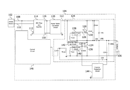
[0017] FIG. 1 is a schematic diagram, partially in block form, of a lamp
system according to
embodiments disclosed herein.
[0018] FIG. 2 is a schematic diagram of a control circuit of the lamp system
of FIG. 1 according
to embodiments disclosed herein.
[0019] FIG. 3 is a flow chart of a method performed by a lamp system to
selectively operate a
lamp between a first lighting level and a second lighting level according to
embodiments
disclosed herein.
6
CA 02766726 2014-12-02
DETAILED DESCRIPTION
[0020] FIG. 1 illustrates a lamp system 100. The lamp system 100 includes an
input power
source, such as but not limited to an alternating current (AC) power supply
102. The lamp
system 100 also includes an electronic ballast 104 (hereinafter ballast 104)
and a lamp 106.
Although the lamp 106 is illustrated in FIG. 1 as a single lamp, in some
embodiments, the lamp
106 may be one lamp or a plurality of lamps connected together in series. In
some embodiments,
the lamp 106 is an electrodeless lamp, such as but not limited to an ICETRON
lamp available
from OSRAM SYLVANIA, a QL induction lamp available from Philips, a GENURA lamp
available from General Electric, or an EVERLIGHT lamp available from
Matsushita. Though
the lamp system 100 is described throughout as energizing an electrodeless
lamp, the lamp
system 100 may be used to energize other types of lamps without departing from
the scope of the
invention.
[0021] The ballast 104 includes a high voltage input terminal (i.e., line
voltage input terminal)
108 adapted to be connected to an alternating current (AC) power supply (e.g.,
standard 120V
AC household power) (such as but not limited to the AC power supply 102). The
ballast 104
also includes a neutral input terminal 110 and a ground terminal 112
connectable to ground
potential. An input AC power signal is received by the ballast 104 from the AC
power supply
102 via the high voltage input terminal 108. The ballast 104 includes an
electromagnetic
interference (EMI) filter and a rectifier (e.g., full-wave rectifier) 114,
which are illustrated
together in FIG. 1. The EMI filter portion of the EMI filter and rectifier 114
prevents noise that
may be generated by the ballast 104 from being transmitted back to the AC
power supply 102.
The rectifier portion of the EMI filter and rectifier 114 converts AC voltage
received from the
AC power supply 102 to DC (direct current) voltage. The rectifier portion
includes a first output
terminal connected to a DC bus 116 and a second output terminal connected to a
ground
potential at ground connection point 118. Thus, the EMI filter and rectifier
114 outputs a DC
voltage on the DC bus 116.
[0022] A power factor correction circuit 120, which may, in some embodiments,
be a boost
converter, is connected to the first and second output terminals of the EMI
filter and rectifier
114. The power factor correction circuit 120 receives the rectified DC voltage
and produces a
high DC voltage on a high DC voltage bus ("high DC bus") 122. For example, the
power factor
7
CA 02766726 2014-12-02
correction circuit 120 may provide a voltage of around 450 volts to the high
DC voltage bus 122.
An inverter circuit 124 having an inverter input is connected to the power
factor correction
circuit 120 to receive the high DC voltage and convert it to AC voltage. The
inverter circuit 124
has an inverter output adapted to connect to the lamp 106 to selectively
provide AC current to
the lamp 106 to energize the lamp 106.
100231 In the lamp system 100 as shown in FIG. 1, the inverter circuit 124
includes a half-bridge
resonant inverter. Alternatively, in some embodiments, other self-oscillating
inverter circuits
may be used. In particular, the inverter circuit 124 includes a switching
circuit to operate at a
switching frequency to convert the DC voltage received by the inverter circuit
124 to AC
voltage. In some embodiments, the switching circuit includes a first switching
component Q1
and a second switching component Q2, as shown in FIG. 1. For example, the
first and second
switching components Q I, Q2 may each comprise a metal¨oxide¨semiconductor
field-effect
transistor (MOSFET). As such, the first switching component Q1 has a gate
terminal 126, a
drain terminal 128, and a source terminal 130. Similarly, the second switching
component Q2
has a gate terminal 132, a drain terminal 134, and a source terminal 136. A
first gate drive
circuit 138 is connected at the gate terminal 132 of the first switching
component Q1, and a
second gate drive circuit 140 is connected at the gate terminal 132 of the
second switching
component Q2. An inverter start-up circuit 142 is connected at the drain
terminal 134 of the
second switching component Q2 to initially activate the second switching
component Q2. Once
the second switching component Q2 is initially turned on by the inverter start-
up circuit 142, the
first and second switching components Ql, Q2 are complementarily commutated
via first and
second gate drive circuits 138, 140. In other words, the switching circuit is
operated such that
when the first switching component Q1 is conductive (e.g., ON), the second
switching
component Q2 is non-conductive (e.g., OFF). Likewise, when the second
switching component
Q2 is conductive (e.g., ON), the first switching component Q1 is non-
conductive (e.g., OFF).
[00241 The inverter circuit 124 includes a resonant circuit comprising an
inductor LREs and a
capacitor CREs connected together in series. The resonant circuit LREs, CREs
is connected to the
source terminal 130 of the first switching component Q1 via a DC blocking
capacitor CDC. The
resonant circuit LRES, CRES provides a high voltage to ignite the lamp 106 and
a magnitude-
limited current to operate the lamp 106 at a particular current. In some
embodiments, a capacitor
Czys is connected between the drain terminal 128 and the gate terminal 126 of
the first switching
8
CA 02766726 2014-12-02
component Q1 to improve EMI and ensuring zero voltage switching. The lamp
system 100 also
includes an inverter protection circuit 144 connected to the high DC bus 122
via resistors R44 and
R45. The inverter protection circuit 144 detects an overvoltage condition. In
some embodiments,
the inverter protection circuit 144 senses the AC voltage signal being
provided to the lamp 106 via
feedback capacitors C29 and C30 and shuts down the inverter circuit 124 if the
AC voltage exceeds a predefined threshold value. For example, the inverter
protection circuit
144 is able to shut down the inverter circuit 124 when there is no lamp 106
connected to the
ballast 104, because the lamp 106 is not present or because wires used to
connect the lamp 106 to
the ballast 104 have become disconnected.
[0025] A feedback circuit is connected to the inverter output to drive the
switching circuit as a
function of the lamp current and lamp voltage at the inverter output. In
particular, the feedback
circuit provides an output signal having a magnitude and phase for supporting
free oscillations in
the inverter circuit 124. In FIG. 1, the feedback circuit includes a feedback
transformer having a
primary winding T51A, a first secondary winding T51B, and a second secondary
winding T51C,
along with serial capacitors C29 and C30. The primary winding T51A is coupled
to the lamp 106
via the serial capacitors C29 and C30. The first secondary winding T51B is
connected between
source terminal 136 of the first switching component Q1 and the first gate
drive circuit
138. The second secondary winding T51C is connected between source terminal
136 of the second
switching component Q2 and the second gate drive circuit 140. A capacitor C30,
which is
connected across the primary winding T51A of the feedback transformer, acts as
a compensation
capacitor to adjust the phase of the voltage across the second secondary
winding T51C. A detailed
description of an exemplary feedback circuit is set forth in US Patent No.
6,819,057 to
Alexandrov.
[0026] The inverter circuit 124 also includes an impedance component, such as
a capacitor C19,
connected in parallel with the primary winding T51A of the feedback
transformer. It is to be
noted that while the impedance component is illustrated and discussed herein
as the capacitor C19,
the impedance component could include multiple capacitors or other types of
impedance
components known in the art without departing from the scope of the invention.
A control circuit
146 is connected to the inverter circuit 124 via the capacitor C19. The
control circuit 146 is
configured to selectively operate capacitor C19 between a first state and a
second state. In the first
state, the capacitor C19 is enabled (e.g., an operative component of the
inverter circuit 124).
9
CA 02766726 2014-12-02
In the second state, the capacitor C19 is disabled (e.g., a non-operative
component of the inverter
circuit 124). When the capacitor C19 is enabled, the switching circuit
operates at a switching
frequency in a first frequency range, and a first lamp current is provided to
the lamp 106. When
the capacitor C19 is disabled, the switching circuit operates at a switching
frequency in a second
frequency range, and a second lamp current is provided to the lamp 106. When
the capacitor
C19 is enabled rather than disabled, it acts as an additional impedance source
connected in
parallel with the primary winding T51A of the feedback transformer. As such,
the first
frequency range is lower than the second frequency range, and the,first lamp
current is greater
than the second lamp current. In some embodiments, the first frequency range
is 195-205 kHz,
and the first lamp current is about 365-380 mA. The second frequency range is
215-220 kHz,
and the second lamp current is about 300-310 mA. Accordingly, the lamp 106
operates at a first
lighting level when the capacitor C19 is enabled, and at a second lighting
level when the
capacitor C19 is disabled. The first lighting level produces a greater amount
of lumens than the
second lighting level, and thus the first lighting level appears brighter than
the second lighting
level.
[0027] FIG. 2 is a circuit schematic of the control circuit 146 of FIG. 1,
showing greater detail.
In FIG. 2, the control circuit 146 includes a switch S1 at a first control
circuit input terminal to
selectively connect the control circuit 146 to the high voltage input terminal
108 shown in FIG.
1. A first diode D1, having an anode and a cathode, is connected at the
cathode to the switch S1
to prevent current from flowing from the control circuit 146 back to the power
supply 102. The
anode of the diode D1 is connected via a resistive network R1, R2 to a gate
terminal 148 of a
first transistor Ml. When the switch S1 is conductive (e.g., ON), the control
circuit 146 is
connected to the power supply 102, and a positive voltage exists at the anode
of the first diode
Dl. Accordingly, the first diode D1 conducts current through the resistive
network R1, R2. The
resistive network R1, R2 acts as a voltage divider, with the gate terminal 148
of the first
transistor M1 being connected between the resistors R1 and R2. The resistor R2
and a source
voltage of the first transistor M1 are connected to a ground potential. Thus,
the current through
the resistor R2 generates a voltage across the gate terminal 148 and a source
terminal 152 of the
first transistor Ml. The first transistor M1 is conductive (e.g., ON) while
the generated gate-to-
source voltage exists. The control circuit 146 may include one or more
capacitors, such as a
capacitor Cl, to filter and smooth the generated gate-to-source voltage. As
such, when the
CA 02766726 2014-12-02
switch S1 is conductive (i.e., connected to the high voltage input terminal
108), the first
transistor M1 is conductive (e.g., ON).
[0028] The control circuit 146 has a second control circuit input terminal
that is connected to the
DC bus 116. A resistive network R3, R4, R6 reduces the DC voltage received
from the DC bus
116 by the control circuit 146. A capacitor C2 filters the DC voltage received
from the DC bus
116 by the control circuit 146. As shown in FIG. 2, a drain terminal 150 of
the first transistor
M1 is connected to the DC bus 116 via the resistors R3 and R6. A resistor R5
is connected
between the resistor R4 and the capacitor C2 to operate as a current limiter.
A gate resistor R7 is
connected in parallel with the capacitor C2. A Zener diode D2 is connected in
parallel with the
resistor R7 and the capacitor C2. The Zener diode D2 is also connected to a
second transistor
M2. In particular, a cathode of the Zener diode D2 is connected to a gate
terminal 153 of the
second transistor M2, and an anode of the Zener diode D2 is connected to
ground potential.
When the first transistor M1 is conductive, the gate terminal 153 of the
second transistor M2 is
pulled low, thereby turning the second transistor M2 off (non-conductive).
Thus, when the
switch S1 is conductive (i.e., connected to the high voltage input terminal
108), the first
transistor M1 is conductive and the second transistor M2 is not conductive. As
a result, the
capacitor C19 is disabled so no additional impedance is added in parallel with
the primary
winding T51A of the feedback transformer, and the lamp 106 operates at a high
frequency,
producing a low light level output (i.e., low lumen output).
[0029] On the other hand, when the first transistor M1 is not conductive,
there is sufficient (e.g.,
threshold) gate voltage to turn the second transistor M2 ON (conductive).
Thus, when the switch
S1 is not conductive (i.e., disconnected from the high voltage input terminal
108), the first
transistor M1 is not conductive and the second transistor M2 is conductive. As
a result, the
capacitor C19 is enabled and thereby adds impedance in parallel with the
primary winding T51A
of the feedback transformer, so that the lamp 106 operates at a low frequency,
producing a high
light level output (i.e., high lumen output).
[0030] FIG. 3 is a flow chart of steps performed by the lamp system 100 as
described above with
regards to FIGs. 1-2. Of course, the steps described in FIG. 3 may be
performed by other
embodiments of the lamp system 100 that selectively operate a lamp connected
thereto between a
first lighting level (e.g., high lumen output) and a second lighting level
(e.g., low lumen output).
At 202, a self-oscillating inverter circuit provides lamp current to the lamp.
The lamp current
11
CA 02766726 2014-12-02
provided to the lamp is a function of the switching frequency of the inverter
circuit. At 204, a
feedback transformer controls the switching frequency of the inverter circuit.
In particular, the
lamp current provided to the lamp is a function of the switching frequency of
the inverter circuit.
At 206, a control circuit enables an impedance component connected in parallel
with the
feedback transformer, so that the inverter circuit is operated at a switching
frequency in a first
frequency range. At 208, the control circuit disables the impedance component
connected in
parallel with the feedback transformer, so that the inverter circuit is
operated at a switching
frequency in a second frequency range. The first frequency range is lower than
the second
frequency range, so the lamp operates at the first lighting level when the
impedance component
is enabled, and the lamp operates at the second lighting level when the
impedance component is
disabled. As described above, in some embodiments, the control circuit may be
configured to
enable the impedance component when the control circuit is disconnected from
the AC power
supply, and to disable the impedance component when the control circuit is
connected to the AC
power supply.
[0031] In alternative embodiments, the control circuit 146 may be embodied as
a set of
instructions that are executed within a microprocessor, microcontroller, or
the like. In such
embodiments, the control circuit 146 may enable and/or disable the capacitor
C19, and thus
control whether the lamp 106 is illuminated at the first lighting level or at
the second lighting
level, by, for example, operating a switch that connects/disconnects the
capacitor C19 from the
primary winding T51A of the feedback transformer. In such embodiments, the set
of instructions
may be stored within a memory device that is part of the control circuit 146
or that is a separate
component from the control circuit 146. The set of instructions may include,
but is not limited
to, the steps shown in FIG. 3, and may, in some embodiments, include computer
programming
code that, when executed on a processor within the control circuit 146, cause
the control circuit
146 to perform the actions described throughout. Further, in such embodiments,
the control
circuit 146 may be located within the ballast 104, as shown in FIG. 1, or may
be external to the
ballast 104 but otherwise connected to the ballast 104 via, for example but
not limited to, a
network connection.
[0032] The methods and systems described herein are not limited to a
particular hardware or
software configuration, and may find applicability in many computing or
processing
environments. The methods and systems may be implemented in hardware or
software, or a
12
CA 02766726 2014-12-02
combination of hardware and software. The methods and systems may be
implemented in one or
more computer programs, where a computer program may be understood to include
one or more
processor executable instructions. The computer program(s) may execute on one
or more
programmable processors, and may be stored on one or more storage medium
readable by the
processor (including volatile and non-volatile memory and/or storage
elements), one or more
input devices, and/or one or more output devices. The processor thus may
access one or more
input devices to obtain input data, and may access one or more output devices
to communicate
output data. The input and/or output devices may include one or more of the
following: Random
Access Memory (RAM), Redundant Array of Independent Disks (RAID), floppy
drive, CD,
DVD, magnetic disk, internal hard drive, external hard drive, memory stick, or
other storage
device capable of being accessed by a processor as provided herein, where such
aforementioned
examples are not exhaustive, and are for illustration and not limitation.
[0033] The computer program(s).may be implemented using one or more high level
procedural
or object-oriented programming languages to communicate with a computer
system; however,
the program(s) may be implemented in assembly or machine language, if desired.
The language
may be compiled or interpreted.
[0034] As provided herein, the processor(s) may thus be embedded in one or
more devices that
may be operated independently or together in a networked environment, where
the network may
include, for example, a Local Area Network (LAN), wide area network (WAN),
and/or may
include an intranet and/or the interne and/or another network. The network(s)
may be wired or
wireless or a combination thereof and may use one or more communications
protocols to
facilitate communications between the different processors. The processors may
be configured
for distributed processing and may utilize, in some embodiments, a client-
server model as
needed. Accordingly, the methods and systems may utilize multiple processors
and/or processor
devices, and the processor instructions may be divided amongst such single- or
multiple-
processor/devices.
[0035] The device(s) or computer systems that integrate with the processor(s)
may include, for
example, a personal computer(s), workstation(s) (e.g., Sun, HP), personal
digital assistant(s)
(PDA(s)), handheld device(s) such as cellular telephone(s) or smart
cellphone(s), laptop(s),
handheld computer(s), or another device(s) capable of being integrated with a
processor(s) that
13
CA 02766726 2014-12-02
may operate as provided herein. Accordingly, the devices provided herein are
not exhaustive
and are provided for illustration and not limitation.
100361 References to "a microprocessor" and "a processor", or "the
microprocessor" and "the
processor," may be understood to include one or more microprocessors that may
communicate in
a stand-alone and/or a distributed environment(s), and may thus be configured
to communicate
via wired or wireless communications with other processors, where such one or
more processor
may be configured to operate on one or more processor-controlled devices that
may be similar or
different devices. Use of such "microprocessor" or "processor" terminology may
thus also be
understood to include a central processing unit, an arithmetic logic unit, an
application-specific
integrated circuit (IC), and/or a task engine, with such examples provided for
illustration and not
limitation.
[0037] Furthermore, references to memory, unless otherwise specified, may
include one or more
processor-readable and accessible memory elements and/or components that may
be internal to
the processor-controlled device, external to the processor-controlled device,
and/or may be
accessed via a wired or wireless network using a variety of communications
protocols, and
unless otherwise specified, may be arranged to include a combination of
external and internal
memory devices, where such memory may be contiguous and/or partitioned based
on the
application. Accordingly, references to a database may be understood to
include one or more
memory associations, where such references may include commercially available
database
products (e.g., SQL, Informix, Oracle) and also proprietary databases, and may
also include
other structures for associating memory such as links, queues, graphs, trees,
with such structures
provided for illustration and not limitation.
[0038] References to a network, unless provided otherwise, may include one or
more intranets
and/or the internet. References herein to microprocessor instructions or
microprocessor-
executable instructions, in accordance with the above, may be understood to
include
programmable hardware.
100391 Unless otherwise stated, use of the word "substantially" may be
construed to include a
precise relationship, condition, arrangement, orientation, and/or other
characteristic, and
deviations thereof as understood by one of ordinary skill in the art, to the
extent that such
deviations do not materially affect the disclosed methods and systems.
14
CA 02766726 2014-12-02
[0040] Throughout the entirety of the present disclosure, use of the articles
"a" and/or "an"
and/or "the" to modify a noun may be understood to be used for convenience and
to include one,
or more than one, of the modified noun, unless otherwise specifically stated.
The terms
"comprising", "including" and "having" are intended to be inclusive and mean
that there may be
additional elements other than the listed elements.
[0041] Elements, components, modules, and/or parts thereof that are described
and/or otherwise
portrayed through the figures to communicate with, be associated with, and/or
be based on,
something else, may be understood to so communicate, be associated with, and
or be based on in
a direct and/or indirect manner, unless otherwise stipulated herein.
[0042] Although the methods and systems have been described relative to a
specific embodiment
thereof, they are not so limited. Obviously many modifications and variations
may become
apparent in light of the above teachings. Many additional changes in the
details, materials, and
arrangement of parts, herein described and illustrated, may be made by those
skilled in the art.